Understanding the MOSFET Symbol: Theory and Practical Insights for Engineers
This comprehensive guide discusses the MOSFET symbol, explaining how gate, source, drain, and body connections are represented for N channel and P channel devices. It covers theoretical concepts, practical design guidelines, market trends and emerging technologies.

30 Sep, 2025. 12 minutes read

Key Takeaways
A MOSFET is a transistor with at least three terminals: a gate, source, and drain. The schematic symbol shows these terminals, and a broken channel line indicates an enhancement-mode device while a solid line indicates a depletion-mode device.
For enhancement-mode MOSFETs, the arrow points inward for N-channel types and outward for P-channel types. N-channel types use electrons as carriers and turn on with a positive gate voltage, while P-channel types use holes as carriers and turn on with a negative gate voltage.
MOSFETs have a gate insulated from the channel, which connects the source and drain. An N-channel MOSFET conducts only when the gate-to-source voltage exceeds the threshold, creating an electron channel.
The MOSFET's body is typically connected to the source to prevent a parasitic bipolar transistor from activating. This connection creates a body diode between the drain and source that is useful for managing inductive loads.
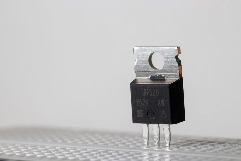
MOSFETs are a fundamental component of modern electronics, with billions used in microprocessors and memory. The power MOSFET market, valued at $7.2 billion in 2023, is projected to reach $11.1 billion by 2030, driven by the demand for energy-efficient devices, electric vehicles, and industrial automation.
Introduction
Metal–oxide–semiconductor field‑effect transistors (MOSFETs) have become the fundamental switching elements in digital logic, analog amplification, and power conversion. Their popularity arises from the insulated gate structure that enables extremely high input impedance and low power consumption. Over the decades, the MOSFET symbol has evolved to encode information about the device’s construction, mode of operation, and polarity. For engineers and students, decoding this symbol is crucial for understanding circuit schematics and selecting suitable devices.
This article explains the theoretical background behind the MOSFET symbol, explores how physical structure and operation map to schematic representation, and offers practical guidance for selecting and using MOSFETs in digital design, hardware engineering, and power electronics. We begin by reviewing MOSFET structure and modes of operation, then examine how the schematic symbol conveys this information for N‑channel and P‑channel devices. Subsequent sections discuss symbol variations, common design considerations, modern power MOSFET technologies, and emerging trends.
MOSFET Fundamentals
Structure of a MOSFET
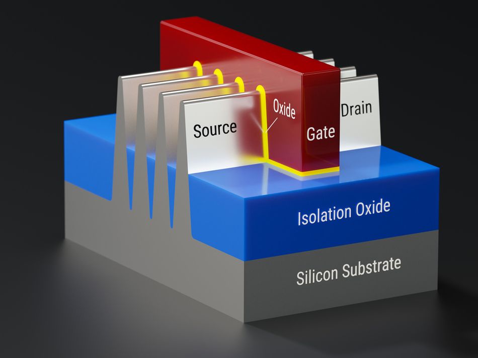
The MOSFET is a four‑terminal device consisting of a gate (G), drain (D), source (S), and body (B). The physical implementation differs between N‑channel and P‑channel devices, but the conceptual structure is similar. An MOS transistor has gate, drain, source, and body terminals, and digital circuits often tie the body to the lowest or highest supply voltage to simplify the device to a three‑terminal symbol.
At the heart of a MOSFET is a lightly doped semiconductor substrate. Two heavily doped regions form the source and drain, separated by a lightly doped “channel” region beneath a thin gate oxide. Applying a voltage to the gate creates an electric field that attracts carriers and modulates the channel conductivity.
The gate electrode is electrically isolated from the channel by silicon dioxide, giving the device extremely high input impedance and enabling voltage‑controlled operation. The MOSFET thus behaves as a voltage‑controlled resistor; no steady current flows into the gate, but the gate voltage controls the drain current.
Suggested Reading: N-Channel MOSFET Basics: Theory, Operation and Practical Implementations
Operating modes
MOSFETs come in two polarities—N‑channel (NMOS) and P‑channel (PMOS)—and two modes—enhancement and depletion. In enhancement‑mode devices, the channel does not exist until a sufficient gate‑to‑source voltage (Vgs) is applied.
For NMOS transistors, electrons form the conduction channel only when Vgs exceeds the threshold voltage (Vth), causing current to flow from drain to source.
PMOS devices require a negative gate bias relative to the source to form a channel; conduction begins when the magnitude of Vgs exceeds the (negative) threshold voltage.
In depletion‑mode MOSFETs, the channel is pre‑doped and conducts at zero gate bias; applying the appropriate gate polarity depletes carriers and turns the device off.
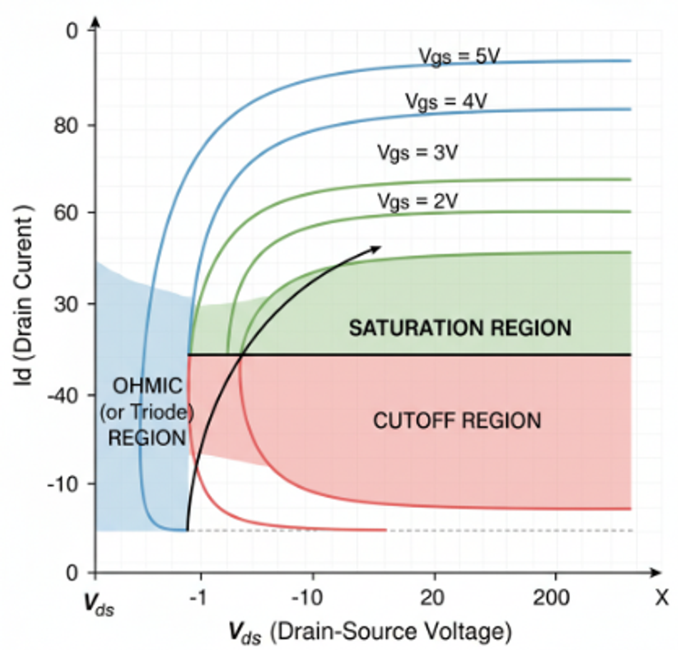
During normal operation, MOSFETs operate in three regions:
Cutoff: Vgs is below Vth (NMOS) or above Vth (PMOS). No channel forms, and the device is off. Drain current is nearly zero.
Linear (ohmic) region: Vgs exceeds Vth, and the drain‑to‑source voltage (Vds) is small. The channel behaves like a resistor whose resistance decreases with increasing Vgs. The drain current is proportional to both Vgs and Vds.
Saturation region: As VDS increases to the point where the channel pinches off, the drain current becomes independent of VDS. The square‑law expression shows that the drain current depends on (Vgs – Vth)². This region is essential for analog amplification and digital switching because the MOSFET behaves as a controlled current source.
Intrinsic Body Diode and Parasitics
Because the body region is doped opposite to the source and drain, a parasitic bipolar transistor can form if the body potential floats. In discrete MOSFETs, the body is therefore shorted to the source, ensuring the parasitic transistor’s base is tied to its emitter and preventing unwanted latch‑up. This connection also creates an intrinsic body diode between the drain and source.
The diode is oriented from source to drain (anode to cathode) in N‑channel devices; it allows current to flow when the MOSFET is reverse-biased, providing free‑wheeling paths for inductive loads. However, the body diode typically has a high forward voltage drop and is slower than purpose‑built diodes, so circuit designers often add external diodes or synchronous rectification MOSFETs to improve efficiency.
MOSFETs also exhibit capacitances between terminals. Data sheets often specify the input capacitance (CISS), output capacitance (COSS) and reverse‑transfer capacitance (CRSS). These correspond to the physical gate‑to‑source (CGS), gate‑to‑drain (CGD) and drain‑to‑source (CDS) capacitances, which must be charged or discharged during switching. The dynamic response of these capacitances, along with package inductance and resistance, determines switching speed and power losses.
Suggested Reading: How Do MOSFETs Work: Comprehensive Technical Guide for Engineers (2025)
Decoding the MOSFET Symbol
Channel Line and Mode Indicator
The MOSFET symbol represents the physical channel as a line between the drain and source terminals. A solid, continuous line indicates a depletion-mode MOSFET, meaning the channel is normally conductive and a gate voltage is required to turn it off.
A broken or dotted line signifies an enhancement‑mode device; the channel does not exist without a gate bias, and the transistor is normally off.
Recognizing this difference is crucial when reading schematics or selecting devices for specific applications.
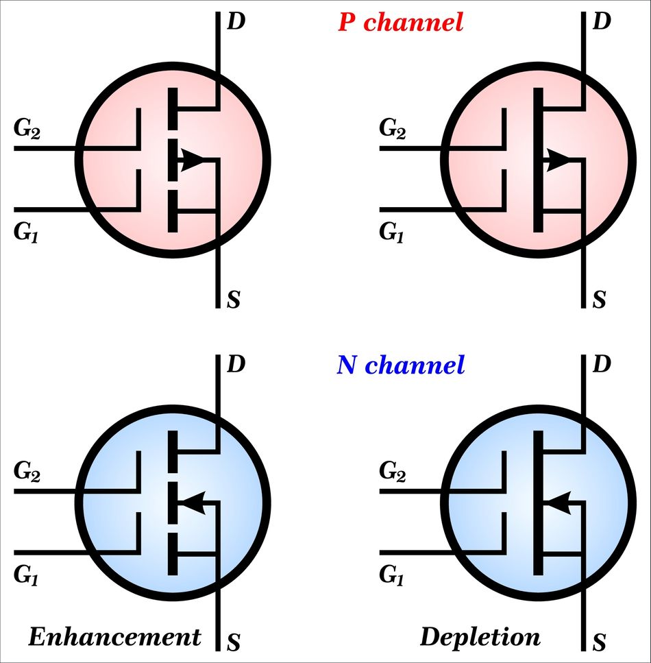
Arrow Orientation and Polarity
The arrow in a MOSFET symbol conveys polarity by showing the direction from P‑type to N‑type material. On symbols that explicitly show the body, the arrow attaches to the body connection and points toward the channel for N‑channel devices. Conversely, in P‑channel devices, the arrow points away from the channel.
Source, Drain and Gate Identification
When the terminals are not labeled, details of the symbol help identify the source, drain, and gate. For enhancement‑ and depletion‑mode symbols, the source is connected to the triangle (arrow) or the body connection, while the gate is drawn parallel to the channel and closer to the source than to the drain.
Knowing which terminal is which is essential because the threshold voltage and conduction direction depend on the polarity of Vgs and Vds. In digital CMOS logic, the source of NMOS devices usually connects to ground (low supply), and the source of PMOS devices connects to VDD (high supply), aligning with the natural direction of current flow in complementary MOS circuits.
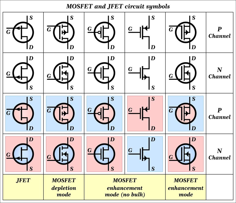
Examples of MOSFET Symbols
The symbols for NMOS and PMOS MOSFETs are different. The NMOS symbol has a broken channel line and an arrow pointing inward, while the PMOS symbol has the arrow pointing outward. Both show gate, drain, and source terminals. This schematic representation helps designers quickly determine polarity and connection in complex circuits.
Practical Interpretation of MOSFET Symbols
Reading N‑channel and P‑channel Symbols
For digital design engineers, interpreting an NMOS symbol begins with identifying the gate, drain and source.. The arrow indicates an N‑channel device when it points toward the channel. Since the drain is typically at a higher potential than the source, the symbol is usually drawn with the drain at the top and the source at the bottom. In enhancement‑mode NMOS circuits, the device conducts when the gate voltage exceeds the threshold voltage, creating a low‑resistance path between drain and source.
For PMOS devices, the arrow points away from the channel. They conduct when the gate voltage is sufficiently below the source voltage (i.e., a negative gate‑to‑source bias). Understanding this relationship is critical when designing complementary MOS (CMOS) logic, where PMOS transistors pull outputs high and NMOS transistors pull outputs low.
Suggested Reading: PMOS vs NMOS: Unraveling the Differences in Transistor Technology
Enhancing and Depleting Channels in the Symbol
Enhancement‑mode symbols use dotted channel lines to signify that the channel does not exist until gate bias is applied. In practice, this means the MOSFET behaves as an open circuit with infinite resistance until the gate voltage crosses the threshold. Designers use enhancement‑mode MOSFETs for switching applications because they have extremely low on‑resistance when turned on and effectively infinite off‑resistance. Depletion‑mode symbols use solid channel lines; these devices conduct at zero gate bias, acting like resistors. Applying the appropriate gate polarity depletes carriers and turns the transistor off, providing normally on functionality.
Recommended Reading: Circuit Symbols: A Comprehensive Guide for Electronics Engineers
Body Diode Representation
Some schematic symbols explicitly show the MOSFET’s intrinsic body diode as a diode symbol in parallel with the channel. This diode is oriented from source to drain for NMOS devices and from drain to source for PMOS devices. The body diode arises because the body connection shorts the P region to the source, preventing a parasitic bipolar transistor from turning on and inadvertently latching the MOSFET.
Designers must account for this diode when using MOSFETs in H‑bridge or half‑bridge circuits, especially in motor drives and DC–DC converters. Synchronous rectification uses an actively controlled MOSFET in place of a diode to reduce conduction losses and improve efficiency.
Bulk Connection and Four‑terminal Symbols
In integrated circuits, the MOSFET’s body is often a common substrate shared by many transistors. Schematic symbols sometimes omit the bulk connection to avoid clutter, relying on arrow orientation to indicate polarity.
For discrete MOSFETs, the body is tied to the source, but in advanced processes, designers may intentionally bias the bulk to modify threshold voltage (body effect). Four‑terminal symbols explicitly show the body (also called bulk or substrate) connection with an arrow pointing from P to N. Recognizing four‑terminal symbols is important in analog design, where body biasing is used to adjust device characteristics.
Choosing MOSFETs for Practical Applications
Selecting an appropriate MOSFET requires balancing multiple parameters: on‑state resistance (Rds(on)), gate charge (Qg), threshold voltage (Vth), maximum drain current, breakdown voltage (VDS), gate‑source voltage rating, and package. The MOSFET symbol itself hints at some of these attributes (polarity, mode), but designers must examine data sheets for quantitative values.
On‑state Resistance and Gate Charge
Low Rds(on) reduces conduction losses in switching applications but often comes at the cost of increased gate charge and capacitance. Device manufacturers optimize Rds(on) using larger die area, special cell geometries, and advanced doping profiles. For example, super‑junction MOSFETs overcome the silicon limit, where Rds(on) increases rapidly with breakdown voltage.
Threshold Voltage and Gate Drive
The threshold voltage (Vth) determines when a MOSFET begins to conduct. For logic‑level NMOS devices, Vth is typically 1–3 V, allowing them to switch directly from microcontroller outputs. Power MOSFETs may have higher thresholds (4–6 V) and require dedicated gate driver circuits to ensure fast transitions.
PMOS thresholds are negative, requiring the gate to be pulled below the source by at least |Vth|. Engineers should ensure the gate drive voltage stays within the absolute maximum ratings to avoid oxide breakdown or body diode conduction.
Safe Operating Area and Thermal Design
The safe operating area (SOA) of a MOSFET defines combinations of drain voltage and current that the device can handle without damage. Exceeding these limits can lead to avalanche breakdown, thermal runaway, or secondary breakdown.
Power MOSFET packages such as TO‑220, D2PAK, or modern clip‑bonded packages have low thermal resistance and help dissipate heat. In high‑frequency switching converters, the gate charge and output capacitance also contribute to dynamic power losses; selecting devices with low Qg and optimizing gate driver design minimizes these losses.
Recommended Reading: Next-generation MOSFET technology Meets Demand for Strong Thermal Performance in Automotive Applications.
Body diode considerations
The body diode’s forward voltage drop (typically 0.7–1.2 V for silicon devices) affects conduction efficiency in synchronous rectifiers and half‑bridge circuits. Wide‑bandgap devices such as silicon carbide (SiC) and gallium nitride (GaN) MOSFETs exhibit smaller body diode losses or incorporate Schottky diodes to improve efficiency.
Packaging and Parasitics
For high‑power applications, the MOSFET’s package influences both thermal and electrical performance. Wire bonding introduces parasitic inductance that can slow switching and cause voltage overshoot, while advanced packages like copper clip or flip‑chip reduce inductance and improve thermal conductivity.
Recommended Reading: The Designers Guide to MOSFET and GaN FET Applications
Modern MOSFET Technologies
Power MOSFET structures
Power MOSFETs differ from small‑signal devices because they must handle high voltages and currents. They use vertical structures that separate the conduction path from the gate plane. Common topologies include V‑MOS, trench (UMOS), and super‑junction structures. Trench MOSFETs use deep trenches to create vertical channels, enabling low on‑resistance and high cell density.
Super‑junction MOSFETs further improve the trade‑off between breakdown voltage and Rds(on) by using alternating P and N columns. These devices dominate high‑voltage, high‑efficiency power supplies and motor drives.
Wide‑bandgap MOSFETs
Silicon MOSFET technology is approaching physical limits for breakdown voltage and switching performance. Wide‑bandgap semiconductors like silicon carbide (SiC) and gallium nitride (GaN)offer higher breakdown fields, lower switching losses and higher temperature capability.
SiC MOSFETs are typically vertical devices similar to silicon power MOSFETs but with much lower on‑resistance and faster switching. GaN transistors often use a high‑electron mobility transistor (HEMT) structure rather than a traditional MOSFET, but some GaN devices incorporate a gate oxide and share similar symbols.
Integration and trench technologies
Modern microprocessors and memory chips integrate billions of MOSFETs into a single die. These devices are typically planar or FinFET transistors with extremely small dimensions. FinFETs extend the MOSFET concept by wrapping the gate around a vertical fin to enhance electrostatic control, reducing leakage and enabling further scaling.
Although FinFETs use a three‑dimensional structure, their schematic symbol remains largely the same—a transistor symbol with source, drain, and gate. Additional design considerations, such as body biasing and threshold adjustment, are often abstracted away in circuit symbols and integrated design flows.
CMOS logic and digital design
Complementary metal–oxide–semiconductor (CMOS) logic pairs PMOS and NMOS transistors in pull‑up and pull‑down networks. When the input is low, the PMOS conducts and pulls the output high; when the input is high, the NMOS conducts and pulls the output low. This arrangement ensures near‑zero static power dissipation because only leakage current flows when the logic state is stable.
The MOSFET symbol is critical in CMOS circuit diagrams to differentiate between the P‑channel and N‑channel devices and to understand the conduction path. In integrated circuits, the body of NMOS transistors is often tied to ground, while the body of PMOS transistors connects to Vdd. Recognizing these implicit connections helps designers avoid the body effect and ensure correct threshold voltages.
Suggested Reading: Nexperia's MLPAK MOSFETs: The Right Fit for Scalable, Application-Driven Designs
Market Trends and Adoption of MOSFETs
MOSFET technology has transformed electronics by enabling high‑density integration and efficient power conversion. Billions of MOSFETs are incorporated into modern microprocessors, memory devices, and logic chips, providing basic switching functions for digital circuits. Power electronics also rely on MOSFETs for efficient motor drives, DC–DC converters, inverters, and RF amplifiers. The widespread adoption of electric vehicles, renewable energy systems, and battery‑powered devices continues to drive innovations in MOSFET technology.
Market research from Persistence Market Research forecasts some interesting facts about MOSFET adoption:
- The global power MOSFET market will expand from approximately US$7.2 billion in 2023 to US$11.1 billion by 2030, representing a compound annual growth rate (CAGR) of about 6.3 %.
- Growth drivers include the demand for energy‑efficient electronics, increased production of electric vehicles, expanding industrial automation, and miniaturization of consumer electronics.
However, the market also faces challenges such as semiconductor supply chain disruptions and raw material shortages. Engineers should stay abreast of these trends because supply constraints and new technologies (like SiC and GaN devices) impact component availability and design strategies.
Conclusion
The MOSFET symbol condenses complex semiconductor physics into a simple schematic representation. Understanding the relationship between the symbol and the device’s structure, polarity, and operating mode is essential for engineers and students designing digital logic, analog amplifiers, or power converters. The arrow orientation, channel line style, and body connection reveal whether the device is N‑channel or P‑channel, enhancement‑mode or depletion‑mode, and whether a body diode is present. Recognizing these details helps prevent design errors and simplifies the process of selecting appropriate transistors.
MOSFET technology continues to evolve. Innovations such as super‑junction structures, trench geometries, wide‑bandgap materials, and advanced packaging push the boundaries of efficiency, power density, and switching speed. At the same time, the global power MOSFET market is expanding due to the demand for energy‑efficient electronics, electric vehicles and industrial automation. By mastering the MOSFET symbol and staying informed about emerging technologies, engineers can harness the full potential of this versatile transistor in their designs.
FAQs
1. What does the arrow in the MOSFET symbol mean?
The arrow indicates the direction from the P‑type to the N‑type semiconductor. In N‑channel devices, the arrow points toward the channel, following the mnemonic “n is in,” while in P‑channel devices, the arrow points outward.
2. How do I differentiate between enhancement‑ and depletion‑mode MOSFET symbols?
Enhancement‑mode symbols use broken or dotted channel lines, indicating the channel does not exist at zero gate bias. Depletion‑mode symbols use solid lines, indicating a normally on channel.
3. What is the purpose of the body diode?
Connecting the MOSFET’s body to the source prevents a parasitic bipolar transistor from turning on, but it also creates an intrinsic diode from source to drain. This diode is useful for free‑wheeling current in inductive circuits but has a relatively high forward voltage and slow recovery time.
4. Why tie the MOSFET body to the source in discrete devices?
Shorting the body (substrate) to the source eliminates the floating P region and prevents latch‑up. This connection is implicit in three‑terminal symbols and ensures the correct body bias.
5. How do super‑junction MOSFETs reduce on‑resistance?
Super‑junction structures use alternating p‑ and n‑type columns in the drift region. When voltage is applied, depletion regions from adjacent columns merge laterally, enabling higher doping levels and reducing RdsRDS(on) compared with planar MOSFETs.
6. What is the difference between NMOS and PMOS operation?
NMOS devices conduct when VgsVGS is positive relative to the source and exceed the threshold voltage; electrons are the majority carriers. PMOS devices conduct when VgsVGS is negative relative to the source; holes are the majority carriers and the threshold voltage is negative.
References
"The MOSFET and Metal Oxide Semiconductor Tutorial," Electronics Tutorials. [Online]. Available: https://www.electronics-tutorials.ws/transistor/tran_6.html
"MOSFET," Wikipedia. [Online]. Available: https://en.wikipedia.org/wiki/MOSFET
"MOSFET Structure and Operation for Analog IC Design," All About Circuits. [Online]. Available: https://www.allaboutcircuits.com/technical-articles/mosfet-structure-and-operation-for-analog-ic-design/
"What are Super Junction MOSFETs?," Shindengen Electric Manufacturing Co., Ltd. [Online]. Available: https://www.shindengen.com/products/semi/column/basic/mosfet/what_are_super_junctions.html
"MOSFET Symbols," PC Basic. [Online]. Available: https://www.pcbasic.com/blog/mosfet_symbols.html
"Power MOSFET Market," Persistence Market Research. [Online]. Available: https://www.persistencemarketresearch.com/market-research/power-mosfet-market.asp