Understanding NPN vs PNP Transistors: A Comprehensive Guide
This article delves into the specifics of NPN and PNP transistors, their working principles, applications, comparisons, and factors to consider when choosing between them.

Last updated on 19 Dec, 2023. 18 minutes read
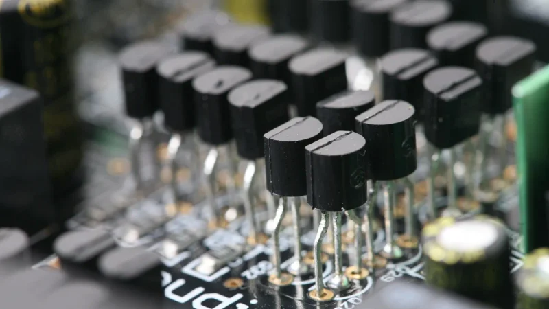
Transistors etched on PCB
Introduction to Transistors
The invention of the transistor in the 1940s was a major turning point in the history of electronics. Transistors replaced bulky and unreliable vacuum tubes, making it possible to build smaller, more powerful, and more efficient electronic devices. Their invention also led to the development of IC, which further miniaturized electronic devices and made them even more powerful. Today, they're an integral part of electronic devices, facilitating circuit miniaturization and boosting device performance.
Transistors are made of semiconductor materials, which have properties of both conductors and insulators. This allows them to control the flow of electricity, making them ideal for amplifying and switching signals. Comparing NPN vs PNP transistors is key to understanding transistors. This NPN vs PNP distinction shapes their roles in circuits. Each type, made of three layers - emitter, base, and collector - operates differently. The base, notably thin, is sandwiched between the other layers. The transistor can be either a PNP type or an NPN type, depending on the arrangement of the p-type and n-type semiconductors.
The operation of NPN vs PNP transistors involves the movement of charge carriers, electrons, and holes. The flow of these charge carriers through the transistor can be controlled by a small input current or voltage, which then controls a larger output current or voltage. This property of transistors allows them to be used as amplifiers or switches. Transistors have revolutionized the way we live and work, and they continue to play a vital role in the development of new technologies.
Basics of Transistors
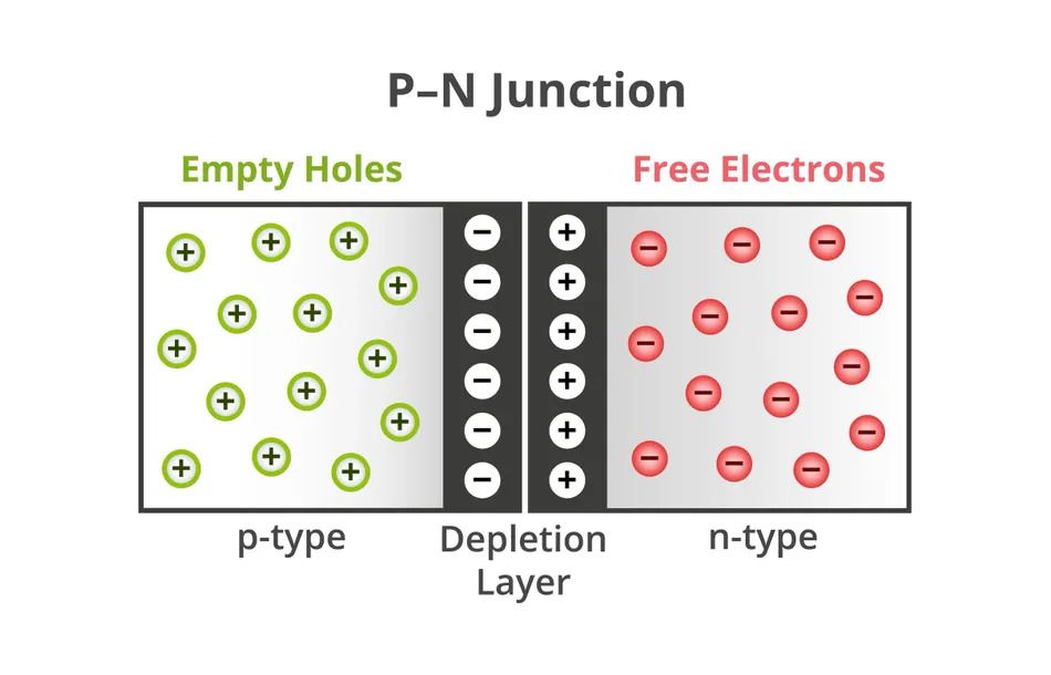
A transistor is a semiconductor device that controls the flow of current or voltage and acts as a switch or gate for electronic signals. It is composed of three layers of semiconductor material, each of which can conduct electricity. The semiconductor material is given special properties through a chemical process called doping. The doping process results in a material that either has extra electrons (N-type) or holes (P-type), which are vacancies for electrons.
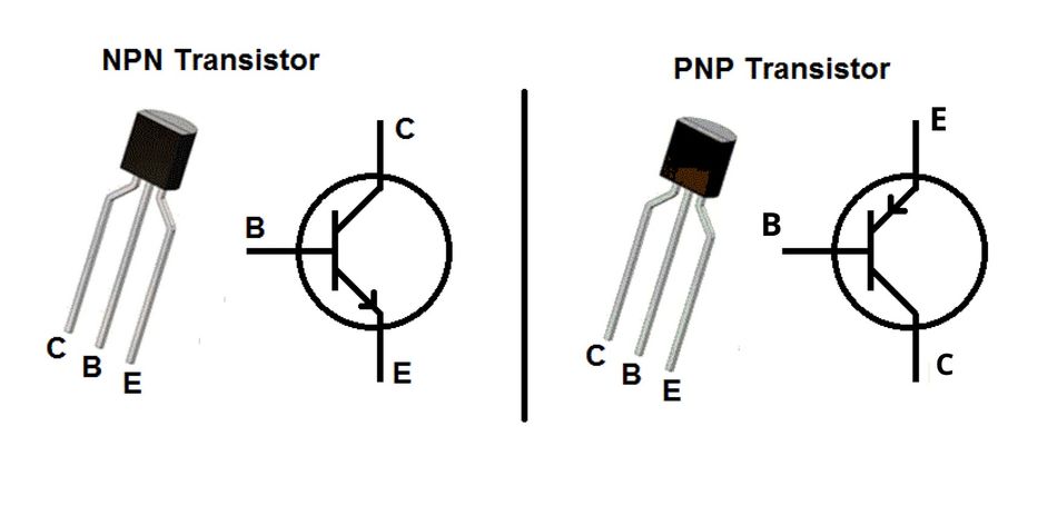
The transistor is made up of three layers: the emitter, base, and collector. [1] The arrangement of these layers distinguishes the two main types of transistors: NPN and PNP. In an NPN transistor, a thin layer of P-type material (the base) is sandwiched between two N-type layers (the emitter and the collector). In a PNP transistor, a thin layer of N-type material is sandwiched between two P-type layers.

A transistor functions by using a small current that flows between the emitter and the base to control the much larger current flow between the collector and the emitter. The base-emitter current determines the number of charge carriers (electrons or holes) that can cross the base-collector junction, thereby controlling the current flow between the collector and the emitter.
Transistors can operate in three different modes: active, cutoff, and saturation. In the active mode, the transistor can amplify signals. If the emitter-base junction is not at least 0.6-0.7 volts when observing the terminals of a BJT, the transistor is in the cutoff region. In the cutoff mode, the transistor acts as an open switch between the collector and the emitter. In the saturation mode, the transistor acts as a closed switch between the collector and the emitter.
Transistors are integral components in a vast array of electronic devices because of their ability to function as amplifiers, switches, and oscillators. Their versatility and reliability have made them indispensable in the field of electronics.
Types of Transistors
Transistors are classified into different types based on their structure, functionality, and applications. The two primary types of transistors are Bipolar Junction Transistors (BJTs) and Field Effect Transistors (FETs).
Bipolar Junction Transistors are further divided into NPN and PNP transistors. The NPN transistor consists of two n-type semiconductor materials separated by a thin layer of p-type. In contrast, the PNP transistor consists of two p-type semiconductors separated by a thin layer of n-type. NPN transistors are the most widely used because they provide superior performance in most electronic circuits due to the greater mobility of electrons compared to holes.
Field Effect Transistors are another major type of transistor, which are further divided into Junction Gate Field-Effect Transistors (JFETs) and Metal Oxide Semiconductor Field Effect Transistors (MOSFETs). Unlike BJTs, which are current-controlled, FETs are voltage-controlled devices. This means that the output current in FETs is controlled by the input voltage. JFETs are seldom used in modern electronics, while MOSFETs are widely used due to their high input impedance and low power consumption.
In addition to these two types, the Insulated-Gate Bipolar Transistor (IGBT) is yet another type of transistor that combines the high input impedance of a MOSFET with the high current-carrying capability of a BJT. IGBTs are commonly used in power electronics, such as inverters and electric motor drives.
Finally, the FinFET is a type of MOSFET that uses a 3D structure to improve control of the current flow, enabling further miniaturization and improved performance. [2] FinFETs are used in the latest generation of microprocessors and memory chips.
Each type of transistor has its unique characteristics and applications. For example, BJTs are used in amplifiers and oscillators for their high gain, while MOSFETs are used in digital circuits and power amplifiers for their high switching speed and efficiency. Understanding these different types of transistors and their properties is crucial for selecting the right transistor for a specific application.
Recommended Reading: Understanding Transistors: What They Are and How They Work
Understanding NPN Transistors
NPN transistor is a type of bipolar junction transistor (BJT) that is composed of two layers of N-type semiconductor material, with a layer of P-type material sandwiched in between. The term NPN is derived from the sequence of these semiconductor layers.
The three layers of the NPN transistor correspond to three regions: the emitter, the base, and the collector. The emitter is the region on one side that emits electrons or holes (depending on the type of transistor) into the base. The base is the middle region, which is thin and lightly doped. The collector is the region on the other side that collects these charge carriers from the base.
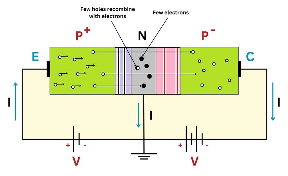
The operation of an NPN transistor is based on the movement of electrons as the majority charge carriers. When a small current is applied to the base-emitter junction (forward-biased), it allows a larger current to flow from the collector to the emitter (reverse-biased). This property of controlling a large output current with a small input current makes the NPN transistor a useful device for amplification and switching applications.
Understanding the structure, and operation of NPN transistors is crucial for anyone involved in electronics, whether it's designing circuits, troubleshooting devices, or studying semiconductor physics.
Working Principle of NPN Transistors
The working principle of an NPN transistor is based on the control of current flow between the emitter and collector regions by varying the base current. The NPN transistor has three terminals: the emitter (E), the base (B), and the collector (C). The emitter is made of N-type material, the base is made of P-type material, and the collector is made of N-type material.
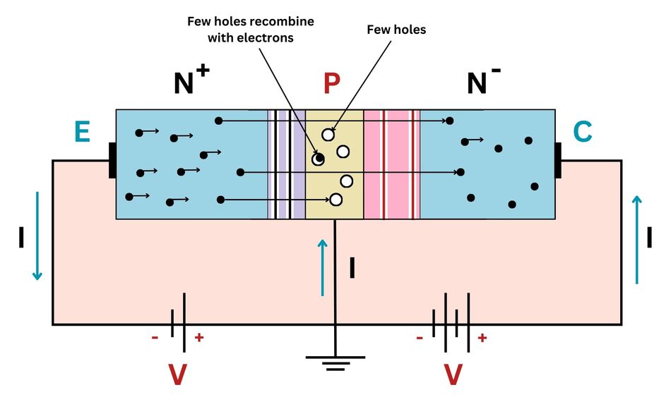
When a small positive voltage is applied to the base-emitter junction, the junction becomes forward-biased, allowing electrons to flow from the emitter to the base. Since the base region is thin and lightly doped, only a small fraction of these electrons recombine with holes in the base. The majority of the electrons continue to flow through the base and reach the collector, which is reverse-biased.
The reverse-biased base-collector junction creates an electric field that repels the electrons away from the base and attracts them toward the collector. As a result, a large current flows from the collector to the emitter, which is controlled by the smaller base current. The ratio of the collector current to the base current is known as the current gain (β) of the transistor. [3]
The NPN device operates in three different regions, depending on the biasing conditions:
Active region: In this region, the base-emitter junction is forward-biased, and the base-collector junction is reverse-biased. The transistor operates as an amplifier, with the output current proportional to the input current.
Cutoff region: In this region, both the base-emitter and base-collector junctions are reverse-biased. The transistor is in the "off" state, and no current flows between the collector and emitter.
Saturation region: In this region, both the base-emitter and base-collector junctions are forward-biased. The transistor is in the "on" state, and the maximum current flows between the collector and emitter.
Understanding NPN output is essential for designing and analyzing electronic circuits that use these devices for amplification, switching, and other applications.
Applications of NPN Transistors
NPN transistors are versatile electronic components with a wide range of applications. Their ability to amplify weak signals and act as efficient switches makes them indispensable in many electronic devices and systems.
One of the primary applications of NPN transistors is in amplification circuits. They are used in audio amplifiers, radio frequency (RF) amplifiers, and operational amplifiers. In these applications, the transistor amplifies a weak input signal to produce a larger output signal. For instance, in an audio amplifier, the NPN transistor can amplify the weak audio signal from a microphone or a music player to drive a loudspeaker.
NPN transistors are also extensively used in digital logic circuits. They are used in logic gates, flip-flops, and other digital circuits to perform binary operations. In these applications, the transistor acts as a switch that turns on or off based on the input signals, thereby performing the logic operation.
Another significant application of NPN transistors is in power electronics. They are used in power amplifiers, voltage regulators, and power supply circuits. In these applications, the transistor controls the flow of large currents and operates at high voltages. For example, in a voltage regulator, the NPN transistor adjusts its resistance based on the input voltage to maintain a constant output voltage.
NPN transistors are also used in oscillators, which generate a continuous output signal of a specific frequency. [4] They are used in radio transmitters, signal generators, and clock circuits. In these applications, the transistor, in combination with other components like resistors, capacitors, and diodes, forms a feedback loop that oscillates at a specific frequency.
They are also used as NPN sensors, that give a low voltage when they detect something. They are commonly used in applications where a sinking output is desired, including PLCs, proximity sensors, capacitive sensors, and photoelectric sensors.
In summary, NPN transistors are fundamental components in a wide range of electronic devices and systems. Their ability to amplify signals and act as switches, combined with their robustness and reliability, makes them a key component in modern electronics. Understanding the datasheet and applications of NPN transistors is crucial for designing and analyzing electronic circuits.
Understanding PNP Transistors
A PNP transistor is another type of bipolar junction transistor (BJT), which is essentially the mirror image of the NPN transistor. It consists of two layers of P-type semiconductor material with a layer of N-type material sandwiched in between. The term PNP comes from the sequence of these semiconductor layers.
The three layers of the PNP transistor correspond to three regions: the emitter, the base, and the collector. The emitter is the region on one side that emits holes into the base. The base is the middle region, which is thin and lightly doped. The collector is the region on the other side that collects these charge carriers from the base.
The operation of a PNP transistor is similar to that of an NPN transistor, but with the roles of the electrons and holes reversed. When a small current is applied to the base-emitter junction (reverse-biased), it allows a larger current to flow from the emitter to the collector (forward-biased). This property of controlling a large output current with a small input current makes the PNP transistor a useful device for amplification and switching applications.
Understanding the structure, and operation of PNP transistors is crucial for anyone involved in electronics, whether it's designing circuits, troubleshooting devices, or studying semiconductor physics.
Working Principle of PNP Transistors
The working principle of a PNP transistor, like its NPN counterpart, is based on the control of current flow between the emitter and collector regions by varying the base current. However, the PNP transistor operates with holes as the majority charge carriers, which is the opposite of the NPN transistor that operates with electrons as the majority charge carriers.
In a PNP transistor, when a small negative voltage is applied to the base-emitter junction, the junction becomes forward-biased. [5] This allows holes to flow from the emitter, which is made of P-type material, to the base, which is made of N-type material. Since the base region is thin and lightly doped, only a small fraction of these holes recombine with electrons in the base. The majority of the holes continue to flow through the base and reach the collector, which is reverse-biased.
The reverse-biased base-collector junction creates an electric field that repels the holes away from the base and attracts them toward the collector. As a result, a large current flows from the emitter to the collector, which is controlled by the smaller base current. The ratio of the collector current to the base current is known as the current gain (β) of the transistor.
The PNP transistor operates in three different regions, depending on the biasing conditions:
Active region: In this region, the base-emitter junction is forward-biased, and the base-collector junction is reverse-biased. The transistor operates as an amplifier, with the output current proportional to the input current.
Cutoff region: In this region, both the base-emitter and base-collector junctions are reverse-biased. The transistor is in the "off" state, and no current flows between the emitter and collector.
Saturation region: In this region, both the base-emitter and base-collector junctions are forward-biased. The transistor is in the "on" state, and the maximum current flows between the emitter and collector.
Understanding PNP output is essential for designing and analyzing electronic circuits that use these devices for amplification, switching, and other applications.
Applications of PNP Transistors
PNP transistors, like NPN transistors, have a wide range of applications in electronic devices and circuits. They are often used in conjunction with NPN transistors to form complementary pairs, which provide several advantages in terms of power efficiency and circuit design.
One of the primary applications of PNP transistors is in complementary push-pull amplifiers. In these circuits, a pair of NPN and PNP transistors work together to amplify an input signal. The NPN transistor amplifies the positive half of the input signal, while the PNP transistor amplifies the negative half. This configuration results in a more efficient and linear amplification of the input signal, reducing distortion and improving the overall performance of the amplifier.
PNP transistors are also used in voltage regulators, particularly in linear voltage regulators. In these circuits, a PNP transistor is used as a pass element to control the output voltage. The transistor adjusts its resistance based on the input voltage and the desired output voltage, maintaining a stable output voltage even when the input voltage or load current changes.
Another application of PNP transistors is in current mirror circuits. These circuits are used to generate a precise copy of a reference current. A PNP transistor and an NPN transistor form a current mirror that can be used to produce a precise current ratio between the input and output currents. Current mirrors are commonly used in analog integrated circuits, such as operational amplifiers and voltage references.
PNP transistors are also used in digital logic circuits, particularly in complementary metal-oxide-semiconductor (CMOS) technology. In CMOS circuits, NPN and PNP transistors are used together to form logic gates, such as inverters, NAND gates, and NOR gates. These logic gates are the basis of control systems, proximity sensors, and industrial control.
PNP sensors output a high-voltage signal when they detect something. This makes it best used in applications where a sourcing output is desired, PLC inputs, and industrial automation systems. They are commonly used in instrumentation applications, pneumatic sensors, and input cards.
In summary, PNP transistors are versatile electronic components with a wide range of applications, often used in conjunction with NPN transistors. Their ability to amplify signals, regulate voltages, and form complementary pairs in various circuits makes them essential components in modern electronics.
Recommended Reading: The First Topological Acoustic Transistor
Comparing NPN and PNP Transistors
NPN and PNP transistors, both types of bipolar junction transistors (BJTs), have similar structures and operating principles but differ in the types of charge carriers they use and the direction of current flow.
The primary difference between NPN and PNP transistors lies in the type of majority charge carriers they use. NPN transistors use electrons as the majority charge carriers, while PNP transistors use holes. This difference in charge carriers leads to a difference in the direction of current flow. In an NPN transistor, the conventional current flows from the collector to the emitter. In contrast, in a PNP transistor, the conventional current flows from the emitter to the collector.
The biasing of NPN and PNP transistors also differs. For an NPN transistor to be in the active region, the base-emitter junction must be forward-biased, and the base-collector junction must be reverse-biased. For a PNP transistor, the opposite is true: the base-emitter junction must be reverse-biased, and the base-collector junction must be forward-biased.
In terms of applications, both NPN and PNP transistors are used in a wide range of electronic devices and circuits. They are often used together in complementary pairs, such as in push-pull amplifiers and CMOS logic gates. NPN and PNP transistors are also used in a variety of automation applications. For example, they can be used to control motors, valves, and other actuators.
The choice between using an NPN or a PNP transistor depends on the specific requirements of the circuit. NPN transistors are generally preferred for their higher electron mobility, which leads to faster switching times and higher frequency operation. However, PNP transistors are often used in high-side switches and voltage regulators due to their ability to handle high voltages.
In conclusion, while NPN and PNP transistors have many similarities, their differences in charge carriers, current direction, biasing, and applications make them suitable for different roles in electronic circuits. Understanding these differences is crucial for selecting the right transistor for a given application.
Example Device Specifications
Below are real datasheet snapshots for popular BJTs. Use them as quick design references.
* **2N3904** — h-FE 100 – 300; V<sub>CE(sat)</sub> ≈ 0.2 V @ I<sub>C</sub> = 10 mA [7]
* **2N3906** — h-FE 100 – 300; V<sub>CE(sat)</sub> ≈ 0.25 V @ I<sub>C</sub> = 10 mA [8]
| Device | V<sub>CE(max)</sub> | I<sub>C(max)</sub> | P<sub>D(max)</sub> | Source |
|-------|-----------|-----------|-----------|--------|
| 2N3904 | 40 V | 200 mA | 625 mW | [7] |
| 2N3906 | 40 V | 200 mA | 300 mW | [8] |
| TIP41C | 100 V | 6 A | 65 W | [9] |
> Noise tip: Low-noise NPNs such as BC550C quote ≈ 2 dB at 1 kHz [10].
> Complementary pair: BC557C is the PNP mate to BC547 and shares the same 45 V rating [11].
Differences in Working Principles
The working principles of NPN and PNP transistors, while similar in many respects, have key differences that originate from the types of semiconductor materials used and the direction of current flow.
In an NPN transistor, the majority of charge carriers are electrons. When a positive voltage is applied to the base-emitter junction, it becomes forward-biased, allowing electrons to flow from the emitter (N-type material) to the base (P-type material). The transistor base is thin and lightly doped, so most of these electrons pass through the base and reach the collector. The collector is reverse-biased, creating an electric field that pulls the electrons from the base to the collector. This results in a large current flowing from the collector to the emitter, controlled by the smaller base current.
In contrast, a PNP transistor operates with holes as the majority charge carriers. When a negative voltage is applied to the base-emitter junction, it becomes forward-biased, allowing holes to flow from the emitter (P-type material) to the base (N-type material). Similar to the NPN transistor, most of these holes pass through the base and reach the collector, which is reverse-biased. The electric field at the base-collector junction pushes the holes from the base to the collector, resulting in a large current flowing from the emitter to the collector, controlled by the smaller base current.
Another key difference lies in the direction of conventional current flow. In an NPN transistor, the conventional current flows from the collector to the emitter, following the direction of electron flow. In a PNP transistor, the conventional current flows from the emitter to the collector, opposite to the direction of electron flow but in the same direction as hole flow.
These differences in working principles between NPN and PNP transistors have implications for their applications. Understanding these differences is crucial for designing and analyzing electronic circuits that use these devices.
Differences in Applications
NPN and PNP transistors, while similar in many respects, have distinct applications due to their unique characteristics. The choice between using an NPN or a PNP transistor in a circuit depends on the specific requirements of the circuit, including the direction of current flow, the type of load, and the desired performance characteristics.
NPN transistors are generally preferred in applications that require high-speed switching and high-frequency operation. This is because electrons, which are the majority charge carriers in NPN transistors, have higher mobility than holes, the majority charge carriers in PNP transistors. The higher electron mobility allows NPN transistors to switch on and off more quickly, making them suitable for high-speed digital circuits and high-frequency analog circuits.
In addition, NPN transistors are commonly used in low-side switches, where the load is connected between the transistor and the positive supply voltage. In this configuration, the emitter terminal of the NPN transistor is connected to the ground, and the transistor switches the current flow to the load. This is a common configuration in power electronics, motor control circuits, and digital logic circuits.
On the other hand, PNP transistors are often used in high-side switches, where the load is connected between the transistor and the ground. In this configuration, the emitter of the PNP transistor is connected to the positive supply voltage, and the transistor switches the current flow from the supply to the load. This is a common configuration in power management circuits, such as voltage regulators and battery chargers.
PNP transistors are also used in complementary push-pull amplifiers, in conjunction with NPN transistors. In these circuits, the NPN transistor amplifies the positive half of the input signal, while the PNP transistor amplifies the negative half. This configuration provides efficient and linear amplification of the input signal, reducing distortion and improving the overall performance of the amplifier.
In summary, while both NPN and PNP transistors have a wide range of applications, their unique characteristics make them suitable for different roles in electronic circuits. Understanding these differences in applications is crucial for selecting the right transistor for a given circuit design.
Recommended Reading: PMOS VS NMOS: Focus on Two Main Forms of MOSFET
Choosing Between NPN and PNP Transistors
The choice between NPN and PNP transistors in a circuit design depends on several factors. One of the primary considerations is the direction of current flow. NPN transistors are typically used in low-side switches, where the load is connected between the transistor and the positive supply voltage. In this configuration, the emitter of the NPN transistor is connected to the ground, and the transistor switches the current flow to the load. This is a common configuration in power electronics, motor control circuits, and digital logic circuits.
On the other hand, PNP transistors are often used in high-side switches, where the load is connected between the transistor and the ground. In this configuration, the emitter of the PNP transistor is connected to the positive supply voltage, and the transistor switches the current flow from the supply to the load. This is a common configuration in power management circuits, such as voltage regulators and battery chargers.
Another consideration is the operating frequency. NPN transistors, which use electrons as the majority charge carriers, have higher electron mobility than PNP transistors, which use holes. The higher electron mobility allows NPN transistors to switch on and off more quickly, making them suitable for high-speed digital circuits and high-frequency analog circuits. [6]
Finally, the specific requirements of the circuit may dictate the choice between NPN and PNP transistors. For instance, if the circuit requires a high voltage rating, a PNP transistor may be a better choice due to its ability to handle high voltages. On the other hand, if the circuit requires fast switching times, an NPN transistor may be preferred due to its higher electron mobility.
Let's summarize their basic differences:
| Parameter | NPN Transistor | PNP Transistor |
| Structure | Two N-type layers separated by one P-type layer | Two P-type layers separated by one N-type layer |
| Direction of Current | Collector to Emitter | Emitter to Collector |
| Majority Charge Carriers | Electrons | Holes |
| Minority Charge Carriers | Holes | Electrons |
| Biasing | Forward | Reverse |
| Ideal For | Sinking Current | Sourcing Current |
| Applications | Amplifiers, Logic Gates, LEDs | Pull-up Circuits, Current Sources, High-Side Loads |
In conclusion, the choice of PNP vs NPN transistors in a circuit design is not a one-size-fits-all decision. It requires a careful consideration of the specific requirements of the circuit, the characteristics of the transistors, and the trade-offs involved.
Conclusion
Choosing between NPN and PNP transistors is a critical decision in electronic circuit design. The choice depends on various factors, including the direction of current flow, the type of load, and the desired performance characteristics. NPN transistors, with their high electron mobility, are generally preferred for high-speed switching and high-frequency operation. On the other hand, PNP transistors are often used in high-voltage applications and when complementary pairs are required for improved power efficiency and circuit design. Understanding these factors and the differences between NPN and PNP transistors is crucial for selecting the right transistor for a given application.
Frequently Asked Questions (FAQs)
1. What is the main difference between NPN and PNP transistors?
A. The main difference between NPN and PNP transistors lies in the type of majority charge carriers they use and the direction of current flow. NPN transistors use electrons as the majority charge carriers, while PNP transistors use holes. In an NPN transistor, the conventional current flows from the collector to the emitter, while in a PNP transistor, it flows from the emitter to the collector.
2. Why are NPN transistors more commonly used than PNP transistors?
A. NPN transistors are more commonly used than PNP transistors because electrons, which are the majority charge carriers in NPN transistors, have higher mobility than holes, the majority charge carriers in PNP transistors. This higher electron mobility allows NPN transistors to switch on and off more quickly, making them suitable for high-speed digital circuits and high-frequency analog circuits.
3. Can NPN and PNP transistors be used interchangeably?
A. While NPN and PNP transistors have similar structures and operating principles, they cannot be used interchangeably due to their differences in charge carriers, current direction, and biasing. The choice between using an NPN or a PNP transistor depends on the specific requirements of the circuit.
4. What are some common applications of NPN and PNP transistors?
A. NPN transistors are commonly used in low-side switches, high-speed digital circuits, and high-frequency analog circuits. PNP transistors are often used in high-side switches, high-voltage applications, and complementary push-pull amplifiers. Both types of transistors are used in a wide range of electronic devices and circuits.
References
[1] Wevolver. Understanding Transistors: What They Are and How They Work [Cited 2023 November 18] Available at: Link
[2] Researchgate. Advantages of FINFET over traditional CMOS [Cited 2023 November 18] Available at: Link
[3] Researchgate. Advantages of FINFET over traditional CMOS [Cited 2023 November 18] Available at: Link
[4] Titan. How Do Transistors Work? Current Flow In N-P-NTransistor [Cited 2023 November 18] Available at: Link
[5] Electronics-tutorials. The Bipolar PNP Transistor [Cited 2023 November 18] Available at: Link
[6] Studysmarter. Bipolar Junction Transistor [Cited 2023 November 18] Available at: Link
[8] **onsemi.** “2N3904 / MMBT3904 NPN Transistor – Datasheet,” Rev. Dec 2021. Available from: https://www.onsemi.com/pdf/datasheet/mmbt3904-d.pdf
[9] **onsemi.** “2N3906 / MMBT3906 PNP Transistor – Datasheet,” Rev. Dec 2021. Available from: https://www.onsemi.com/pdf/datasheet/mmbt3906-d.pdf
[10] **STMicroelectronics.** “TIP41C NPN Power Transistor – Datasheet,” Rev. Apr 2024. Available from: https://www.st.com/resource/en/datasheet/tip41c.pdf
[11] **onsemi.** “BC550C NPN Low-Noise Transistor – Datasheet,” Rev. Jan 2023. Available from: https://www.onsemi.com/pdf/datasheet/bc550-d.pdf
[12] **STMicroelectronics.** “BC557C PNP General-Purpose Transistor – Datasheet,” Rev. May 2024. Available from: https://www.st.com/resource/en/datasheet/bc557c.pdf