How Do Circuit Boards Work: A Comprehensive Guide to the Heart of Electronics
From Blueprint to Functionality: Navigating the Intricacies of Circuit Boards – Manufacturing, Mechanics, and Troubleshooting Demystified

14 Nov, 2023. 14 minutes read
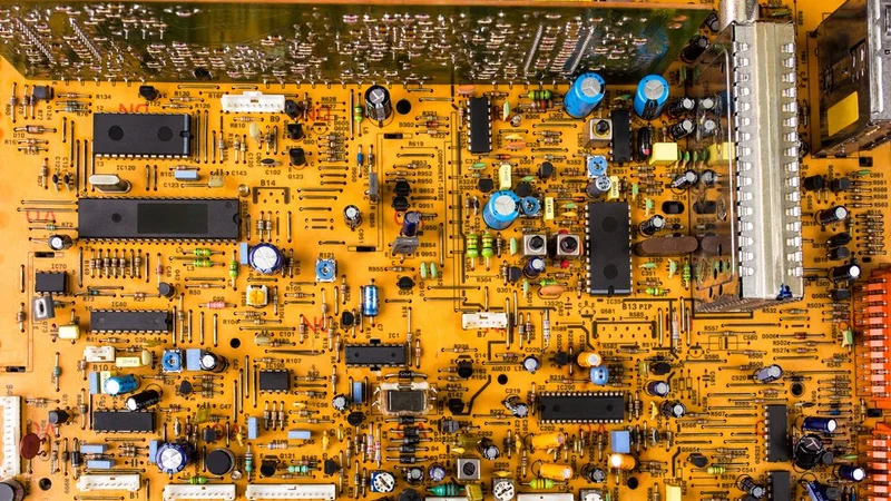
A typical circuit board with components and wiring traces
What are Circuit Boards?
A circuit board is a fundamental component in electronics. It’s the backbone of most electronic devices, providing a platform for the arrangement and interconnection of electronic components.
Circuit boards are found in nearly every electronic device, from simple devices like digital watches and calculators to complex devices like computers and televisions. They are designed to route electric signals through electronics, which allows the device to function as intended. While they can be made manually via soldering techniques, professional circuit boards are made with printing technology, hence their name, Printed Circuit Boards (PCBs).
Recommended Reading: Printed Circuit Boards: Differences Between Rigid, Flex, and Rigid-Flex PCBs
What are Circuit Boards Made of?
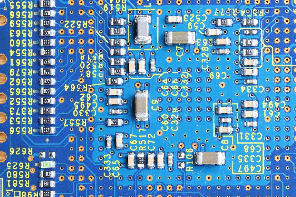
Typically, circuit boards are made from an insulating material, often fiberglass, and are coated with conductive materials. These conductive materials, usually copper, are etched to form pathways that electric currents can follow. These pathways, known as traces, connect the various components on the board, such as resistors, capacitors, and transistors, allowing them to work together to perform complex tasks.
So, a circuit board combines semiconductors, insulators, and conducting materials to achieve a specific objective.
Recommended Reading: What are Circuit Boards Made Of? An Extensive Guide to Materials and Manufacturing Processes
Basic Components of a Circuit Board
A circuit board comprises various components, each with a specific function that contributes to the overall operation of the electronic device. These components are strategically placed and interconnected on the board to form a complete circuit that can perform complex tasks.
Here is a quick look at the essential components of a circuit board:
Resistors
Resistor is the most common component found on a circuit board is the resistor.
They are typically small, cylindrical components with two leads and are often color-coded to indicate their resistance value. The color bands follow a standard code, with each color representing a specific number. By reading the color bands in the correct order, you can determine the resistance value of the resistor.

For PCB mounting, there are two types of resistors, i.e., through-hole and surface-mounted devices (SMD). On a PCB, a resistor occupies a minimal space and is usually present in the form of
- Fixed resistor
- Potentiometer
- Light-dependent resistor (LDR)
Capacitor
Capacitors are another key component of a circuit board. They are used to store and release electrical energy in a circuit. Capacitors consist of two conductive plates separated by an insulating material, known as a dielectric.
For PCB mounting, capacitors come in various types including:
- Axial
- Radial
- Surface mounted
Additionally, the type of a capacitor depends upon, its own specific characteristics and applications. For example, ceramic capacitors are small, inexpensive, and commonly used in high-frequency circuits, while electrolytic capacitors have a high capacitance-to-volume ratio and are used in power supply circuits.
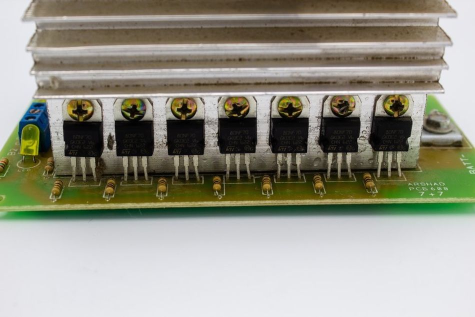
Transistors
Transistors are perhaps the most important components on a circuit board. They function as electronic switches and amplifiers, controlling the flow of electricity through a circuit. A transistor has three layers of semiconductor material and three terminals: the emitter, the base, and the collector.
Transistors can be used in various configurations, such as common emitter, joint base, and standard collector configurations, each with its own unique characteristics and applications. For example, the standard emitter configuration is widely used as an amplifier, while the standard collector configuration is often used as a buffer.
Transistors can be mounted on PCBs in two ways: through-hole and surface mount.
- For through-hole transistors, the leads are inserted into holes in the PCB and then soldered.
- For surface-mount transistors, the leads are soldered to pads on the surface of the PCB.
- When mounting transistors on PCBs, it is important to consider the orientation of the transistor and the heat dissipation requirements.
- Transistors can also be mounted on heat sinks to help dissipate heat.
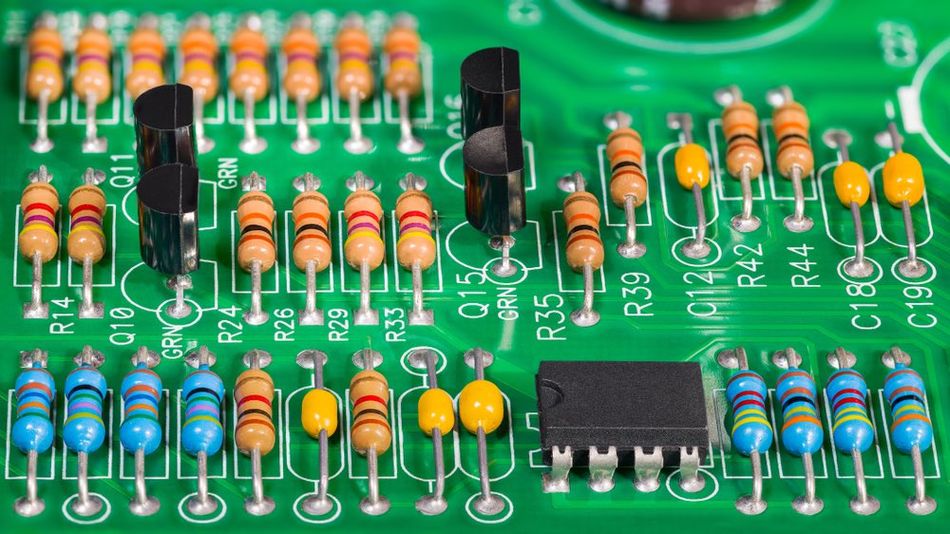 Fig 2: A PCB featuring resistors, capacitors, transistors, and integrated circuits
The Design and Layout of a Circuit Board
The design and layout of a circuit board is a complex process that requires careful planning and precision. It involves arranging the components and routing the electrical connections in a way that optimizes the performance of the circuit while minimizing its size and cost.
Here is how the process works:
Creating a Schematic Design
The first step in designing a circuit board is creating a schematic diagram. This is a symbolic representation of the circuit, showing the components and their connections but not their physical arrangement. The schematic serves as a blueprint for the circuit, detailing the electrical relationships between the components.
Physical Layout Design
Layout design involves placing the components on the board and routing the electrical connections between them. The goal is to arrange the components to minimize the length of the connections and avoid crossing paths, which can lead to interference and signal loss.
This is typically achieved with a computer-aided design (CAD) software. This software lets the designer place the components and route the connections in a virtual environment, making it easier to visualize the layout and adjust as needed. It can also perform checks to ensure that the layout meets specific design rules, such as minimum distances between components and paths.
The layout process often involves a trade-off between performance and size. A compact layout can save space and reduce cost, but it may also lead to a higher density of electrical paths, increasing the risk of interference.
Conversely, a more spread-out layout can improve performance by reducing interference, but it may also increase the size and cost of the board. In exceptional cases like high-performance circuits, multi-board PCB designs can be used to ensure efficiency and consistent performance.
The physical layout design is a crucial part of the entire design process that determines the cost, and functionality of the board in a system. Therefore, it is crucial to avoid PCB design mistakes that can prove costly in the long run.
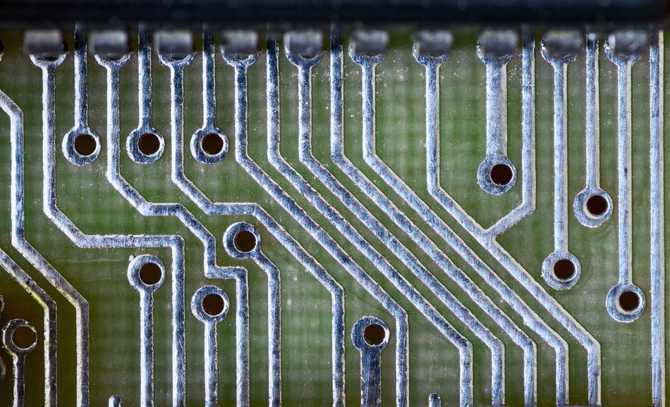
What are Traces in a Circuit?
Traces are the conductive pathways on a circuit board, typically made of copper. They connect various components and allow electrical signals to flow between them. Traces are formed by etching away unwanted copper from the surface of the board, leaving behind the desired pattern of traces.
The design of traces can directly affect the performance of the circuit. They must be carefully routed to minimize the length of the connections and avoid crossing paths, which can lead to interference and signal loss. The width of the traces also plays a crucial role in determining the amount of current they can carry and the amount of resistance they introduce into the circuit.
There are some specialized techniques to equalize trace length that can reduce signal lags in a circuit board. Moreover, several factors must be considered when designing traces, such as the current carrying capacity, signal integrity, and electromagnetic compatibility (EMC).
- Current Carrying Capacity - The current carrying capacity of a trace is determined by its width, thickness, and the temperature rise it can withstand. Wider and thicker traces can carry more current, but they also take up more space on the board and may increase manufacturing costs.
- Signal Integrity - It is another important consideration when designing traces. High-speed signals can be affected by factors such as impedance mismatch, crosstalk, and signal reflections, which can degrade the signal quality and lead to errors in the circuit's operation. To maintain signal integrity, traces carrying high-speed signals should be impedance-matched, and their lengths should be kept as short as possible.
- Electromagnetic Compatibility (EMC)- EMC is the ability of a circuit to function correctly in the presence of electromagnetic interference (EMI) and to minimize the emission of EMI to other devices. To achieve good EMC performance, traces should be routed to minimize the loop area formed by the signal path and its return path, as this can reduce the emission of EMI and increase the circuit's immunity to external EMI.
Further Reading: Trace PCB: A Comprehensive Guide
What are PCB Pads?
Pads are small, flat areas of conductive material on a circuit board that serve as connection points for electronic components. They are typically made of copper and are designed to provide a stable and reliable surface for soldering components to the board. Pads play a crucial role in the assembly and functioning of a circuit board, as they ensure that the components are securely attached and electrically connected to the traces.
There are several types of pads used in circuit board design, each with its own specific purpose and characteristics. Some common types include:
- Through-hole pads: These pads are used for through-hole components, which have leads that pass through holes in the board and are soldered on the opposite side. Through-hole pads are typically circular or oval in shape and are surrounded by a ring of conductive material called an annular ring.
- Surface-mount pads: These pads are used for surface-mount components, which are soldered directly to the surface of the board without passing through holes. Surface-mount pads are typically rectangular in shape and are designed to provide a large surface area for soldering.
- Test pads: These pads are used for testing and debugging purposes during the manufacturing process. They provide convenient access points for measuring voltages, currents, and other electrical properties of the circuit. Test pads are typically small, circular pads that are not connected to any components.
When designing pads for a circuit board, several factors must be considered, such as the size and shape of the pad, the type of component being used, and the soldering process. Moreover, size and shape of the pad should be large enough to accommodate the component lead and provide a sufficient surface area for soldering, but not so large that it takes up unnecessary space on the board or creates soldering difficulties.
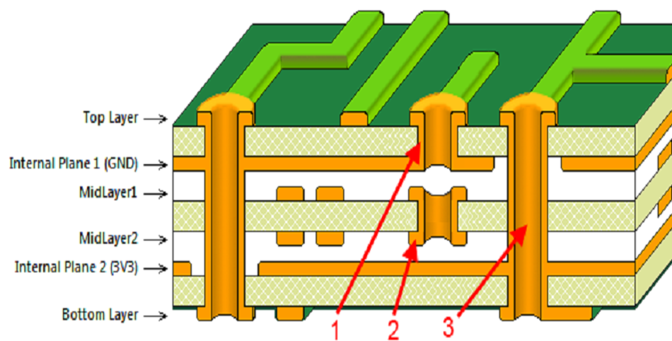
What are Vias in PCB?
Vias are small holes in a circuit board that provide electrical connections between different layers of the board. They are an essential part of multilayer circuit board design, allowing signals and power to be routed between the various layers and components. Vias are typically filled with conductive material, such as copper, to create a reliable and low-resistance connection.
Several types of vias are used in circuit board design, each with its specific purpose and characteristics. Some common types include:
- Through-hole vias: These vias pass through the entire board thickness, connecting the top and bottom layers. They are the most common via type and are used in single-sided and multilayer boards.
- Blind vias: These vias connect an outer layer of the board to one or more inner layers but do not pass through the entire thickness. Blind vias are used in multilayer boards to save space and reduce the complexity of the layout.
- Buried vias: These vias are located entirely within the inner layers of a multilayer board and are not visible from the outer layers. Buried vias are used to connect inner layers without affecting the layout of the outer layers.
Image Source: https://www.hemeixinpcb.com/blind-via.html
The size and shape of the hole are two critical factors to consider when designing vias., The via hole should be large enough to accommodate the conductive material and provide a reliable electrical connection but not so large that it weakens the board or takes up unnecessary space.
The choice of conductive material can also affect the performance of the via, with copper being the most common choice due to its excellent electrical conductivity and compatibility with the board materials.
Further Reading: What are Vias in Pad? Advantages, Limitations, Applications, and Comparison with Conventional Vias
Manufacturing Process of a Circuit Board
The manufacturing process of a circuit board is a multi-step procedure involving various techniques and technologies. It begins with creating the board material, typically a type of fiberglass known as FR4, which provides a rigid and durable substrate for the components and traces.
The board material is coated on one or both sides with a thin layer of copper, which will be used to form the traces.
The circuit board manufacturing process involves the following steps:
- Design
- Fabrication
- Assembly
Circuit Board Design
Designing a circuit board is a meticulous task that requires a deep understanding of electronics, materials science, and manufacturing processes. The design process follows the same order as discussed earlier. Here is a quick summary of the circuit board design phase:
- Step 1 - Schematic diagram creation for symbolic representation of the circuit.
- Step 2- Circuit board layout design
- Step 3 - Placement of Vias
- Step 4 - Design verification and checks
Circuit Board Fabrication
Fabricating a circuit board is a complex process that involves several stages. The first stage is the preparation of the board material. This typically involves cutting a sheet of board material, usually a type of fiberglass known as FR4, to the desired size. The board material is then coated on one or both sides with a thin layer of copper, which will be used to form the traces.
- Circuit Pattern Creation - Pattern creation is done using a process known as photolithography. The copper-clad board is coated with a light-sensitive material called photoresist. The board is then exposed to ultraviolet light through a mask that contains the desired circuit pattern. The light causes the photoresist to harden in the areas exposed to light, protecting the underlying copper from the next stage, etching.
- Etching - Etching is the removal of unwanted copper from the board to leave behind the desired circuit pattern. It’s done with a chemical solution that dissolves the unprotected copper. The hardened photoresist is then removed, leaving behind the copper traces.
- Drilling - Once the circuit pattern has been created, the board is drilled to create holes for the component leads and vias. The holes are then plated via copper electroplating to create electrical connections between different board layers.
- Solder Mask - The next stage is the application of the solder mask. This is a protective layer that covers the entire board except for the pads where components will be soldered. The solder mask prevents solder from adhering to the traces during assembly, ensuring that the components are soldered only to the pads.
- Silkscreen Application - The final stage in the fabrication process is the application of the silkscreen. This is a layer of ink that is printed onto the board to provide labels and markings for the components. The silkscreen helps to guide the assembly process and provides important information for troubleshooting and repair.
Once the fabrication process is complete, the board is tested to ensure that it functions correctly. This involves checking the continuity of the traces and the absence of shorts, as well as testing the functionality of the circuit if components have been assembled.
Assembling the Circuit Board
The assembly of a circuit board is the process of attaching and soldering the electronic components onto the board. This process can be done manually for small-scale production or prototyping, but it is typically automated for large-scale production using a machine known as a pick-and-place machine.
The pick-and-place machine uses a robotic arm to pick up the components from a feeder and place them onto the board in the correct locations. The components are held in place by a small amount of solder paste that is applied to the pads on the board before the components are placed. The solder paste also provides the necessary electrical connection between the component leads and the traces on the board.
Further Reading: Pick and Place Robots: An In-Depth Guide to Their Functionality and Applications
Reflow Oven
Once all the components have been placed on the board, it is sent through a reflow oven, which heats the board to a temperature that melts the solder paste, forming a solid electrical connection between the component leads and the traces on the board. The board is then cooled to solidify the solder and complete the assembly process.
After the reflow process, the board may undergo additional assembly processes, such as the installation of through-hole components. These components have leads that pass through holes in the board and are soldered on the other side. The installation of through-hole components is typically done manually, as it requires more flexibility than the pick-and-place process.
Board Inspection
The assembled board is then inspected to ensure that all components have been correctly installed and that there are no solder bridges or other defects. This inspection can be done visually, but it is often automated using a machine known as an automatic optical inspection (AOI) machine. The AOI machine uses a camera to capture images of the board and software to analyze the images and identify any defects.
Once the board has passed inspection, it is comprehensively tested to ensure that it functions correctly. This can involve applying power to the board and measuring the voltages and currents in the circuit, as well as testing the functionality of the circuit if it is part of a larger system.
Further Reading: PCB Manufacturing Process: Everything You Need to Know
Functioning of a Circuit Board
Electrical signals navigate through the traces upon powering the board, interacting with components along the way. These components modify the signals based on their properties and functions within the circuit. To ensure proper functionality, circuit boards undergo rigorous testing, often employing methods such as the flying probe test (FPT). FPT utilizes software-driven algorithms and a series of flying probes to examine the electrical connections of the board, ensuring integrity and reliability in its operation. Through meticulous design, construction, and testing, circuit boards form the backbone of countless electronic devices, enabling seamless functionality and performance.
Further Reading: Flying Probe Test: An Extensive Guide to the Technology and Applications
Common Issues and Troubleshooting
Circuit boards, like any other electronic devices, can encounter a variety of issues that can affect their performance. These issues can range from simple problems that can be easily fixed to complex issues that require advanced troubleshooting techniques.
Here are some common issues that can occur with circuit boards and some troubleshooting steps that can be taken to resolve them.
Short Circuits
Perhaps the most common issue with circuit boards is a short circuit. A short circuit occurs when there is a direct connection between the power supply and the ground, bypassing the normal path of the circuit. This can cause excessive current to flow through the circuit, damaging the components and the board. To troubleshoot a short circuit, you can use a multimeter to measure the resistance between the power supply and ground. If the resistance is very low, there is likely a short circuit.
Open Circuits
Another common issue is an open circuit. An open circuit occurs when there is a break in the circuit, preventing the flow of current. A multimeter can help identify an open circuit.
Overheating
Overheating is another common issue with circuit boards. Overheating can be caused by excessive current, poor ventilation, or a faulty component. Overheating can damage the components and the board, and it can also cause the board to fail prematurely. To troubleshoot overheating, you can check the temperature of the board and the components with a thermal camera or a temperature probe. Moreover, heat sinks are used with electronic components to absorb excessive heat that prevents the board from burning.
Component Failure
Component failure is another common issue with circuit boards. Components can fail due to age, wear and tear, or excessive voltage or current. Component failure can cause the circuit board to malfunction or fail. To troubleshoot component failure, you can use a multimeter to measure the voltage and current in the circuit. If the voltage or current is out of specification, there is likely a component failure.
Conclusion
Circuit boards are essential components of electronic devices, acting as their foundational infrastructure by facilitating electrical connections between components. Understanding their functioning requires expertise in electronics and electrical engineering, as it involves intricate interactions between electrical signals and various components. Proper design and manufacturing processes are crucial for ensuring the board's efficiency and reliability in device operation. However, circuit boards can encounter issues ranging from simple fixes to complex problems like short circuits, overheating, and component failures, necessitating advanced troubleshooting skills. Addressing these issues demands a systematic approach grounded in deep knowledge of electronics and electrical engineering, coupled with appropriate diagnostic tools. By employing the right techniques, many common circuit board issues can be successfully diagnosed and resolved, ensuring optimal functionality and performance of electronic devices.
FAQs
What is a circuit board?
A circuit board is a platform for routing electrical signals from one point to another. It serves as the backbone of an electronic device, providing the physical infrastructure for the components and the electrical connections between them.
What are the components of a circuit board?
The components on a circuit board include a variety of electronic devices such as resistors, capacitors, inductors, diodes, transistors, and integrated circuits. These components work together to perform the functions of the electronic device.
What is the role of electricity in a circuit board?
Electricity plays a fundamental role in the functioning of a circuit board. It is the driving force that enables the operation of the electronic components and the flow of signals through the circuit.
What are some common issues with circuit boards?
Common issues with circuit boards include short circuits, open circuits, overheating, and component failure. These issues can affect the performance of the circuit board and require troubleshooting to resolve.
How can I troubleshoot a circuit board?
Troubleshooting a circuit board requires a deep understanding of electronics and electrical engineering, as well as a systematic approach to identifying and resolving issues. This can involve using a multimeter to measure the voltage, current, and resistance in the circuit, checking the temperature of the board and the components, and inspecting the components and the traces for any visible damage.
References
What Is a Resistor? | Resistor Fundamentals | Resistor Guide (eepower.com)
High Performance PCB Systems Design and Analysis Guide | Advanced PCB Design Blog | Cadence
Study on PCB Designing Problems and their Solutions | IEEE Conference Publication | IEEE Xplore
Pick And Place Machine in PCB Manufacturing | Their Role & Need (circuits-diy.com)
Six Common PCB Issues and Repairs | Circuits Central (circuits-central.com)