PCB Design: A Comprehensive Guide to Printed Circuit Board Design - Part 2
This comprehensive series delves into the fundamentals of PCB design, including design workflow, signal integrity, manufacturing, testing and debugging, advanced design techniques, and the latest software and tools available for PCB design.

02 Apr, 2024. 22 minutes read
PCB Design and Manufacturing
Introduction
Printed Circuit Board (PCB) design is a crucial aspect of modern electronics, serving as the foundation for the development and manufacturing of electronic devices. PCBs are the backbone of electronic products, providing the necessary interconnections and support for various components. The PCB design process involves creating a layout that optimizes the placement of components, routing of traces, and ensuring the overall functionality and reliability of the circuit.
This series delves into the intricacies of PCB design, covering a wide range of topics essential for both beginners and experienced designers. Here’s the breakdown:
Part one sets the foundation, exploring the workflow of circuit design-from schematic capture to layout and the critical design rule checks. We delved into the analysis of PCB components and layers, evaluating their impact on signal integrity and thermal management.
Part two now focuses on translating PCB design into reality, exploring the intricacies of PCB manufacturing, assembly, testing, and debugging. Finally, we'll navigate the industry's leading PCB design software and tools, setting the path to create high-performance electronic devices.
Let’s proceed with the PCB manufacturing and assembly!
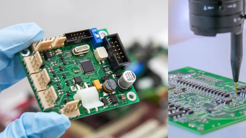
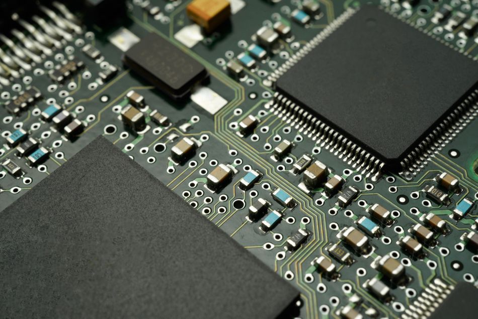
PCB Manufacturing and Assembly
PCB manufacturing and assembly is a complex process that involves several steps, including PCB fabrication, component placement, and soldering. Understanding the manufacturing process and its requirements is essential for creating PCBs that can be reliably produced and assembled.
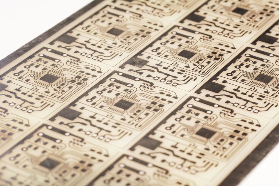
The PCB fabrication process typically involves several steps, including:
PCB design: The PCB design is created using specialized software, which generates the necessary manufacturing files, such as Gerber files and fabrication drawings.
Etching: The PCB substrate is coated with a photosensitive material, which is then exposed to UV light through a photomask. [1] The unexposed areas are etched away, leaving the desired copper traces on the PCB.
Drilling: Holes are drilled through the PCB for component leads and vias.
Plating: The drilled holes are plated with copper to create conductive vias, and the entire PCB is plated with a protective layer, such as solder mask or conformal coating.
Solder mask application: The solder mask is applied to the PCB, covering the copper traces and leaving exposed pads for component placement.
Silkscreen application: The silkscreen is applied to the PCB, providing component labels and other markings for assembly and maintenance.
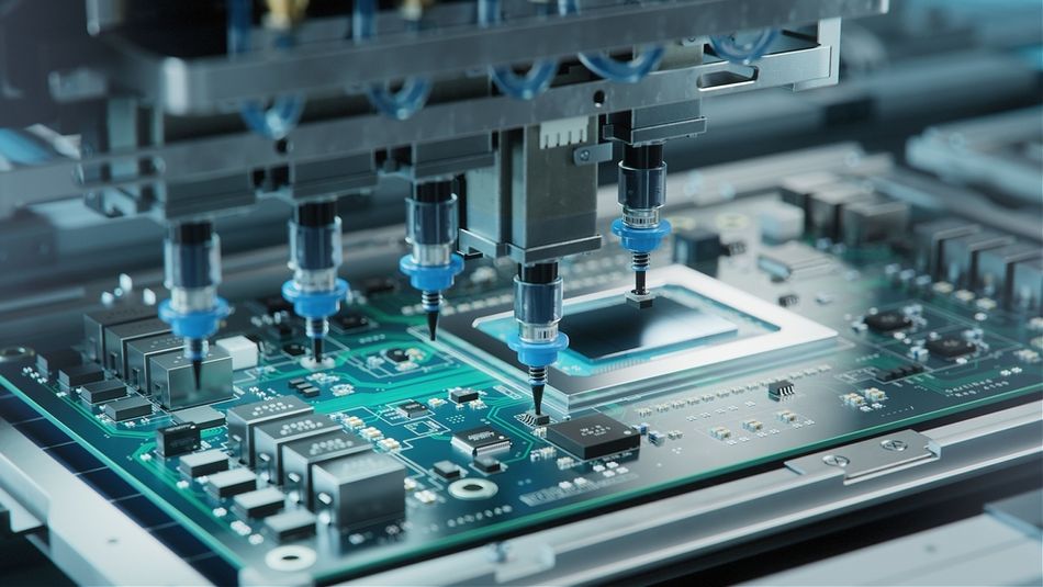
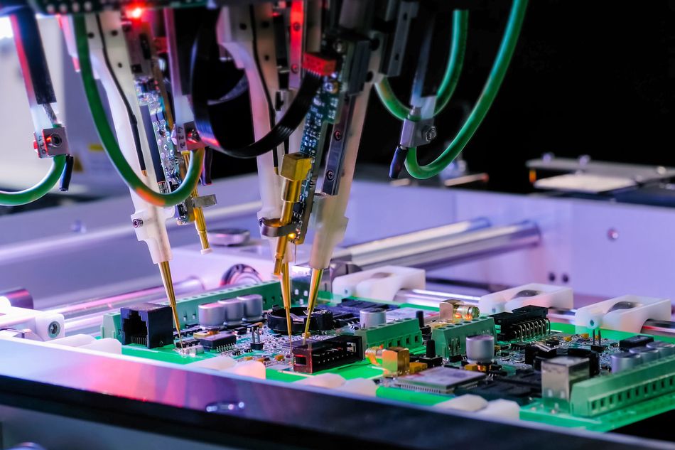
PCB assembly typically involves the following steps:
Component placement: Components are placed on the PCB according to the design specifications.
Soldering: The components are soldered to the PCB, either through wave soldering, reflow soldering, or manual soldering.
Inspection and testing: The assembled PCB is inspected for defects and tested for functionality.
Effective communication and documentation are critical for ensuring a smooth and successful PCB manufacturing and assembly process. Designers must provide clear and accurate manufacturing files, such as Gerber files and fabrication drawings, to the manufacturer. These files should include all necessary information, such as layer stackup, component placement, and drill sizes, to ensure that the PCB can be reliably produced.
Gerber Files and Fabrication Drawings
Gerber files and fabrication drawings are the primary documentation used by PCB manufacturers to produce the physical PCB. Gerber files are a set of vector graphics files that define the PCB's copper layers, solder mask, and silkscreen. Fabrication drawings provide additional information, such as drill sizes, layer stackup, and component placement.
Best practices for creating accurate and complete Gerber files and fabrication drawings include:
Use industry-standard file formats: Gerber files should be created in the RS-274X format, which is widely supported by PCB manufacturers. [2]
Include all necessary layers: Gerber files should include all necessary layers, such as copper layers, solder mask, and silkscreen, to ensure that the PCB can be reliably produced.
Use consistent naming conventions: Use consistent and clear naming conventions for layers and files to avoid confusion and ensure that the correct files are used during production.
Provide accurate dimensions and tolerances: Include accurate dimensions and tolerances in the fabrication drawings to ensure that the PCB meets the required specifications.
Include drill information: Include drill information, such as drill sizes and locations, in the fabrication drawings to ensure that the correct holes are drilled in the PCB.
By following these best practices and providing clear and accurate documentation, designers can ensure a smooth and successful PCB manufacturing and assembly process.
PCB Assembly Techniques
PCB assembly techniques can be broadly categorized into two main types: through-hole and surface mount. Each technique has its own advantages and disadvantages, and the choice of assembly technique depends on the specific requirements of the application.
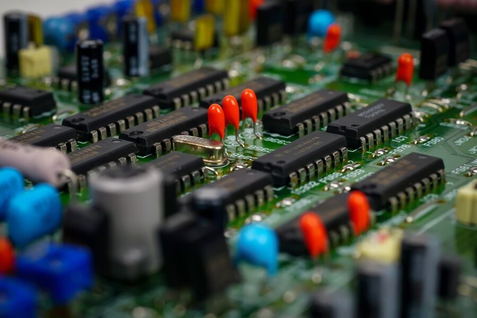
Through-hole assembly involves inserting component leads through holes in the PCB and soldering them on the opposite side. This technique is commonly used for components that require mechanical support or have high power dissipation requirements.
Advantages of through-hole assembly include:
Mechanical support: Through-hole components provide mechanical support to the PCB, making them suitable for applications where the PCB is subjected to mechanical stress.
High power dissipation: Through-hole components can handle higher power dissipation than surface mount components, making them suitable for applications with high power requirements.
Disadvantages of through-hole assembly include:
Limited component density: Through-hole components are larger than surface mount components, limiting the component density that can be achieved on the PCB.
Longer assembly time: Through-hole assembly is a more time-consuming process than surface mount assembly, as it requires manual insertion of components and wave or reflow soldering.
Surface mount assembly involves placing components directly onto the surface of the PCB and soldering them using solder paste and a reflow process. This technique is commonly used for high-density PCBs and applications where space is limited.
Advantages of surface mount assembly include:
High component density: Surface mount components are smaller than through-hole components, allowing for higher component density on the PCB.
Faster assembly time: Surface mount assembly is a faster process than through-hole assembly, as it does not require manual insertion of components and can be automated using pick-and-place machines.
Disadvantages of surface mount assembly include:
Limited mechanical support: Surface mount components do not provide mechanical support to the PCB, making them less suitable for applications where the PCB is subjected to mechanical stress.
Lower power dissipation: Surface mount components typically have lower power dissipation capabilities than through-hole components, making them less suitable for applications with high power requirements.
PCB Assembly Guidelines
When designing PCBs for efficient assembly, designers should consider the following:
Component placement: Arrange components in a way that allows for efficient assembly, such as grouping components by assembly type (through-hole or surface mount) and placing components with similar assembly times close together.
Orthogonal placement: Where possible, arrange components in an orthogonal (grid-like) pattern for easier automated assembly and routing.
Solder mask clearances: Ensure that solder mask clearances are sufficient to allow for proper solder flow and prevent solder bridging.
Drill sizes: Use consistent and appropriate drill sizes for through-hole components to ensure proper fit and prevent damage to the PCB.
Component footprints: Use accurate and consistent component footprints to ensure proper fit and prevent assembly issues.
Detailed documentation: Provide clear and comprehensive design documentation, including component specifications, bill of materials (BOM), and assembly drawings.
By considering these guidelines and the specific requirements of the application, designers can create PCBs that are optimized for efficient assembly and reliable operation.
Recommended Reading: Through Hole vs Surface Mount: Unveiling the Optimal PCB Assembly Technique
PCB Testing and Debugging
PCB testing and debugging are critical steps in the PCB design and manufacturing process, ensuring that the final product meets the required specifications and performs reliably in the intended application. Testing and debugging help identify and resolve issues related to component placement, soldering, signal integrity, and overall functionality.
There are several testing methods used to verify PCB functionality, including:
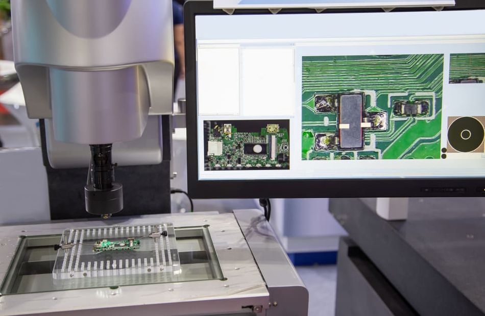
Visual inspection: A visual inspection of the PCB is performed to identify any obvious defects, such as missing or misaligned components, solder bridges, or damaged traces.
Automated optical inspection (AOI): AOI uses cameras and image processing software to automatically inspect the PCB for defects, such as missing components, incorrect component placement, or solder issues.
In-circuit testing (ICT): involves using a bed of nails fixture to make electrical contact with specific points on the PCB, allowing for the testing of individual components and circuits.
Functional testing: Functional testing involves applying power to the PCB and verifying that it performs the intended functions, such as processing signals or communicating with other devices.
Boundary scan testing: Boundary scan testing uses a special test access port (TAP) to test the interconnections between components on the PCB, allowing for the identification of short circuits, open circuits, and other defects. [3]
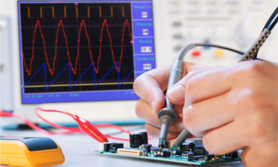
PCB debugging involves using various tools and techniques to identify and resolve issues found during testing. Common tools and techniques used for PCB debugging include:
Oscilloscopes: Oscilloscopes are used to visualize and measure electrical signals on the PCB, helping to identify issues related to signal integrity, noise, and timing.
Logic analyzers: Logic analyzers are used to capture and analyze digital signals on the PCB, helping to identify issues related to digital communication and timing.
Thermal imaging: Thermal imaging cameras are used to identify areas of the PCB that are generating excessive heat, which can indicate issues related to power dissipation or component failure.
Probing: Probing involves using specialized probes to make electrical contact with specific points on the PCB, allowing for the measurement of voltages, currents, and other electrical parameters.
By using a combination of testing methods and debugging techniques, engineers can identify and resolve issues with the PCB design and manufacturing process, ensuring that the final product meets the required specifications and performs reliably in the intended application.
In-Circuit Testing (ICT) and Boundary Scan Testing
In-circuit testing (ICT) and boundary scan testing are two commonly used testing methods for verifying the functionality of PCBs and identifying manufacturing defects.
ICT involves using a bed of nails fixture to make electrical contact with specific points on the PCB, allowing for the testing of individual components and circuits. The bed of nails fixture consists of a series of spring-loaded probes that are arranged to match the test points on the PCB. When the PCB is placed on the fixture, the probes make contact with the test points, allowing for the measurement of voltages, currents, and other electrical parameters.
Benefits of ICT include:
Comprehensive testing: ICT allows for the testing of individual components and circuits, providing a comprehensive assessment of the PCB's functionality.
Early defect detection: ICT can identify manufacturing defects early in the production process, reducing the cost and time associated with rework and repair.
Limitations of ICT include:
Fixture complexity: The bed of nails fixture can be complex and expensive to design and manufacture, particularly for high-density PCBs with many test points.
Limited access: ICT may not be able to access all components on the PCB, particularly those that are located under other components or have limited test points.
Boundary Scan Testing, also known as JTAG testing, uses a special test access port (TAP) to test the interconnections between components on the PCB. The TAP consists of a series of pins that are connected to the boundary scan cells of each component on the PCB. By applying test patterns to the TAP and measuring the response, boundary scan testing can identify short circuits, open circuits, and other defects in the interconnections between components.
Benefits of boundary scan testing include:
Non-intrusive testing: Boundary scan testing does not require physical access to the components on the PCB, making it suitable for testing high-density PCBs with limited test points.
Automated testing: Boundary scan testing can be automated using specialized software, reducing the time and cost associated with manual testing.
Limitations of boundary scan testing include:
Limited component testing: Boundary scan testing can only test the interconnections between components and cannot test the functionality of individual components.
Design requirements: Components must be designed with boundary scan cells to be compatible with boundary scan testing, which can increase the cost and complexity of the PCB design.
In practice, ICT and boundary scan testing are often used in combination with other testing methods, such as functional testing and visual inspection, to provide a comprehensive assessment of the PCB's functionality and identify any manufacturing defects. The choice of testing methods depends on the specific requirements of the application, the complexity of the PCB design, and the available resources for testing and debugging.
Debugging Techniques and Tools
PCB debugging is an essential skill for engineers and technicians involved in the design, manufacturing, and testing of electronic products. Effective debugging requires a combination of knowledge, experience, and the use of appropriate tools and techniques.
Common debugging techniques used in PCB design include:
Visual inspection: A thorough visual inspection of the PCB can often identify obvious defects, such as missing or misaligned components, solder bridges, or damaged traces. This technique is simple but effective and should be the first step in any debugging process.
Continuity testing: Continuity testing involves using a multimeter to check for electrical continuity between two points on the PCB. This technique can identify open circuits, short circuits, and other connectivity issues.
Signal tracing: Signal tracing involves using an oscilloscope or logic analyzer to follow the path of a signal through the PCB, helping to identify issues related to signal integrity, noise, or timing. This technique requires a good understanding of the PCB schematic and the expected behavior of the signals.
Power supply monitoring: Power supply monitoring involves using a multimeter or oscilloscope to measure the voltage and current supplied to the PCB and individual components. This technique can identify issues related to power distribution, such as voltage drops, ripple, or noise.
Thermal analysis: Thermal analysis involves using a thermal imaging camera or temperature probe to identify areas of the PCB that are generating excessive heat. This technique can help identify issues related to power dissipation, component failure, or inadequate cooling.
To perform these debugging techniques effectively, engineers and technicians rely on a variety of tools and equipment, including:
Multimeters: Multimeters are used to measure voltage, current, resistance, and continuity between points on the PCB. They are essential tools for continuity testing and power supply monitoring.
Oscilloscopes: Oscilloscopes are used to visualize and measure time-varying signals on the PCB. They are essential tools for signal tracing and power supply monitoring, providing detailed information about signal amplitude, frequency, and timing.
Logic analyzers: Logic analyzers are used to capture and analyze digital signals on the PCB. They are essential tools for debugging digital circuits, providing information about the state and timing of digital signals.
Thermal imaging cameras: Thermal imaging cameras are used to create a visual representation of the temperature distribution on the PCB. They are useful tools for identifying areas of excessive heat generation and inadequate cooling.
Soldering irons and rework stations: Soldering irons and rework stations are used to repair and modify the PCB, such as replacing components or adding jumper wires. They are essential tools for implementing fixes and modifications identified during the debugging process.
When debugging PCBs, it is important to follow best practices and troubleshooting tips, such as:
Work systematically: Follow a systematic approach to debugging, starting with a visual inspection and proceeding to more advanced techniques as needed. Document each step of the process and the results obtained.
Use the schematic: Always refer to the PCB schematic when debugging, as it provides a roadmap of the circuit and helps identify the expected behavior of signals and components.
Isolate the problem: When a problem is identified, try to isolate it to a specific component or section of the PCB. This can be done by disconnecting or bypassing certain components or by probing signals at various points in the circuit.
Check power and ground: Many PCB issues are related to power and ground, so it is important to check the power supply voltages and the continuity of ground connections early in the debugging process.
Use the right tools: Choose the appropriate tools and equipment for the specific debugging task, and ensure that they are properly calibrated and functioning correctly.
By following these best practices and using the appropriate debugging techniques and tools, engineers and technicians can effectively identify and resolve issues with PCBs, ensuring that the final product meets the required specifications and performs reliably in the intended application.
Recommended Reading: Mastering PCB Testing: Techniques, Methods, and Best Practices Unveiled
Advanced PCB Design Techniques
As electronic systems become more complex and demanding, PCB designers must employ advanced techniques to meet the specific requirements of various applications. These advanced techniques address challenges related to signal integrity, power integrity, electromagnetic compatibility (EMC), and manufacturability.
High-speed digital systems, such as those used in modern computing and communication devices, require careful consideration of signal integrity and timing. Designers must use techniques such as impedance matching, length matching, and proper termination to ensure that signals arrive at their destinations with minimal distortion and jitter.
Radio frequency (RF) and wireless systems, such as those used in cellular phones and IoT devices, require specialized PCB design techniques to minimize signal loss, crosstalk, and interference. Designers must use techniques such as microstrip and stripline routing, ground plane stitching, and proper shielding to ensure that RF signals are transmitted and received with high fidelity.
Mixed-signal systems, which combine analog and digital circuitry on the same PCB, present unique challenges related to noise coupling and signal isolation. Designers must use techniques such as split ground planes, proper component placement, and filtering to minimize the impact of digital noise on sensitive analog circuits.
Emerging trends and technologies in PCB design include the use of advanced materials, such as high-frequency laminates and embedded components, to improve signal integrity and reduce board size. 3D printing and other additive manufacturing techniques are also being explored as a means of creating complex PCB structures and reducing prototyping time. [4]
As PCB design continues to evolve, designers must stay up-to-date with the latest techniques and technologies to ensure that their designs meet the ever-increasing demands of modern electronic systems.
High-Speed PCB Design
High-speed PCB design refers to the design of PCBs for systems that operate at high frequencies, typically above 100 MHz. At these frequencies, the physical properties of the PCB and its components can have a significant impact on signal integrity and timing.
One of the main challenges in high-speed PCB design is managing the impedance of the signal paths. As the frequency of the signal increases, the impedance of the trace becomes more important. If the impedance of the trace does not match the impedance of the source and load, reflections can occur, leading to signal distortion and jitter.
To mitigate these issues, designers must use techniques such as controlled impedance routing, where the width and spacing of the traces are carefully controlled to achieve a specific impedance. Differential signaling, where signals are transmitted as a pair of complementary signals, can also be used to reduce the impact of noise and interference.
Another challenge in high-speed PCB design is managing the propagation delay of signals. As the frequency of the signal increases, the time it takes for the signal to travel from the source to the load becomes more critical. To ensure that signals arrive at their destinations at the correct time, designers must use techniques such as length matching, where the lengths of the traces are carefully matched to ensure that signals arrive at their destinations at the same time.
Other techniques used in high-speed PCB design include the use of ground planes to provide a low-impedance return path for signals, the use of vias to transfer signals between layers, and the use of termination resistors to minimize reflections.
Some best practices for designing high-speed PCBs include:
Use a multi-layer PCB: Multi-layer PCBs provide more routing options and can help reduce crosstalk and interference between signals.
Keep signal traces short: Shorter traces have lower impedance and are less susceptible to noise and interference.
Use ground planes: Ground planes provide a low-impedance return path for signals and can help reduce EMI.
Use differential signaling: Differential signaling can help reduce the impact of noise and interference on signals.
Use proper termination: Proper termination can help minimize reflections and ensure that signals arrive at their destinations with minimal distortion.
By following these best practices and using the appropriate design techniques, PCB designers can create high-speed PCBs that meet the demanding requirements of modern electronic systems.
RF and Mixed-Signal PCB Design
Designing PCBs for radio frequency (RF) and mixed-signal applications requires careful consideration of several factors to ensure optimal performance and minimize interference. RF PCBs must be designed to maintain signal integrity, minimize losses, and prevent unwanted radiation. Mixed-signal PCBs, which contain both analog and digital circuits, must be designed to minimize crosstalk and noise coupling between the two domains.
One of the most important considerations in RF and mixed-signal PCB design is proper grounding and shielding. In RF circuits, a solid ground plane is essential for providing a low-impedance return path for high-frequency currents. This helps to minimize ground bounce and reduce electromagnetic interference (EMI). In mixed-signal circuits, separate ground planes for analog and digital circuits can help to minimize noise coupling between the two domains.
Shielding is another important technique used in RF and mixed-signal PCB design. Shielding involves enclosing sensitive circuits in a conductive enclosure to prevent interference from external sources and to minimize radiation from the circuit itself. This can be achieved through the use of grounded copper pours, conductive gaskets, or dedicated shielding cans.
When designing PCBs for RF and mixed-signal applications, it is important to follow best practices for component placement and routing. Some guidelines for optimizing PCB layout include:
Keep signal traces short: Shorter traces minimize losses and reduce the potential for interference.
Use microstrip or stripline routing: These techniques provide a controlled impedance environment for high-frequency signals.
Avoid sharp bends in traces: Sharp bends can cause reflections and degrade signal integrity.
Use guard rings, and ground pours: These techniques help to isolate sensitive circuits and minimize crosstalk.
Separate analog and digital circuits: Placing analog and digital circuits on opposite sides of the board or using separate ground planes can help to minimize noise coupling.
Use decoupling capacitors: Placing decoupling capacitors close to ICs can help to reduce power supply noise and improve signal integrity.
Pay attention to component placement: Placing components strategically can help to minimize trace lengths and reduce interference.
In addition to these general guidelines, specific considerations may apply depending on the frequency range and application of the PCB. For example, in high-frequency RF circuits, the choice of substrate material and the thickness of the dielectric layer can have a significant impact on signal propagation and losses.
By following best practices for grounding, shielding, and layout, and by carefully considering the specific requirements of the application, PCB designers can create RF and mixed-signal PCBs that deliver optimal performance and reliability.
Recommended Reading: RF PCB: Design, Materials, and Manufacturing Processes
PCB Design Software and Tools
PCB design software and tools play a crucial role in the design and development of modern electronic products. These tools allow designers to create, simulate, and optimize PCB layouts, ensuring that the final product meets the required specifications and performs reliably in the intended application.
There are many PCB design software packages available on the market, ranging from free and open-source tools to high-end commercial solutions. Some of the most popular PCB design software packages include:
Altium Designer: A comprehensive PCB design package that offers schematic capture, 3D modeling, and simulation capabilities. [5]
Cadence Allegro: A powerful PCB design solution that includes advanced routing, signal integrity analysis, and thermal management tools.
Mentor Graphics PADS: A PCB design package that offers schematic capture, layout, and simulation tools, along with a user-friendly interface.
KiCad: A free and open-source PCB design package that includes schematic capture, layout, and 3D modeling tools.
Eagle: A popular PCB design package that offers schematic capture, layout, and autorouting capabilities, along with a large component library.
When choosing a PCB design software package, it is important to consider the specific requirements of the project, such as the complexity of the design, the required features and capabilities, and the available budget. Some factors to consider include:
Ease of use: The software should have a user-friendly interface and intuitive workflow, allowing designers to quickly and easily create and modify PCB layouts.
Component libraries: The software should include a comprehensive library of components, including both generic and manufacturer-specific parts.
Simulation and analysis tools: The software should include tools for simulating and analyzing the performance of the PCB, such as signal integrity analysis, thermal analysis, and electromagnetic compatibility (EMC) analysis.
Collaboration and version control: The software should support collaboration and version control, allowing multiple designers to work on the same project simultaneously and track changes over time.
Output and manufacturing support: The software should be able to generate standard output files, such as Gerber and drill files, and support common manufacturing processes, such as panelization and solder mask generation.
By choosing the right PCB design software and tools for the specific requirements of the project, designers can streamline the design process, reduce development time and costs, and ensure that the final product meets the highest standards of quality and reliability.
Schematic Capture and Simulation Tools
Schematic capture and simulation tools are essential components of the PCB design process, allowing designers to create and validate the logical design of the circuit before moving on to the physical layout.
Schematic capture tools allow designers to create a graphical representation of the circuit, using symbols to represent components and lines to represent connections. This graphical representation is then used to generate a netlist, which describes the connectivity of the components in the circuit.
Simulation tools allow designers to analyze the behavior of the circuit under different operating conditions, such as different input signals, load conditions, and environmental factors. This allows designers to identify potential issues with the circuit, such as signal integrity problems, power supply issues, or thermal concerns, and make necessary modifications before moving on to the physical layout.
Some of the most commonly used schematic capture and simulation tools include:
Altium Designer: Altium Designer includes a powerful schematic capture tool that supports hierarchical design, multi-sheet schematics, and design reuse. It also includes a range of simulation tools, such as SPICE simulation, signal integrity analysis, and power integrity analysis.
Cadence OrCAD: OrCAD is a popular schematic capture and simulation tool that includes a range of features, such as hierarchical design, multi-sheet schematics, and design reuse. It also includes a range of simulation tools, such as PSpice for analog and mixed-signal simulation, and Sigrity for signal and power integrity analysis.
Mentor Graphics PADS: PADS includes a schematic capture tool that supports hierarchical design and multi-sheet schematics, as well as a range of simulation tools, such as HyperLynx for signal integrity analysis and FloTHERM for thermal analysis.
KiCad: KiCad is a free and open-source schematic capture and simulation tool that includes a range of features, such as hierarchical design, multi-sheet schematics, and design reuse. It also includes a SPICE simulator for analog and mixed-signal simulation.
By using schematic capture and simulation tools, designers can streamline the PCB design process in several ways:
Early validation: By simulating the behavior of the circuit early in the design process, designers can identify and correct potential issues before moving on to the physical layout, reducing the risk of costly redesigns later in the process.
Design reuse: Schematic capture tools that support hierarchical design and design reuse allow designers to create modular, reusable components that can be easily incorporated into new designs, reducing development time and costs.
Collaboration: Schematic capture tools that support multi-sheet schematics and version control allow multiple designers to work on the same project simultaneously, improving collaboration and reducing the risk of errors.
Documentation: Schematic capture tools generate a range of documentation, such as netlists, bills of materials (BOMs), and design reports, that can be used to communicate the design to other stakeholders, such as manufacturers and electronics engineer.
By leveraging the capabilities of schematic capture and simulation tools, PCB designers can create high-quality designs that meet the specific requirements of the application, while reducing development time and costs.
PCB Layout and Routing Tools
PCB layout and routing tools are essential for creating the physical design of a PCB, including the placement of components, the routing of traces, and the generation of manufacturing files. These tools allow designers to create complex, high-density layouts that meet the specific requirements of the application, while ensuring manufacturability and reliability.

Modern PCB layout and routing tools offer a range of capabilities, including:
Component placement: Tools for placing components on the PCB, including support for automated placement, design rule checking (DRC), and 3D visualization.
Trace routing: Tools for routing traces between components, including support for manual and automated routing, differential pair routing, and length matching.
Plane creation: Tools for creating power and ground planes, including support for split planes, copper pours, and thermal relief.
Manufacturing file generation: Tools for generating manufacturing files, such as Gerber files, drill files, and pick-and-place files, that can be used by PCB manufacturers to fabricate the board.
One of the key advantages of using PCB layout and routing tools is the ability to automate certain tasks, such as component placement and trace routing. Automated placement tools can quickly and efficiently place components on the board based on a set of predefined rules, such as component spacing and orientation. Automated routing tools can route traces between components based on a set of predefined rules, such as trace width, spacing, and length matching.
Using automated placement and routing tools can significantly reduce the time and effort required to create a PCB layout, while also improving the quality and consistency of the design. However, it is important to use these tools effectively and to review the results carefully to ensure that the design meets the required specifications.
Some tips for effectively using PCB layout and routing software include:
Use design rules: Define and use design rules, such as minimum trace width and spacing, to ensure that the layout meets the required specifications and is manufacturable.
Use constraints: Define and use constraints, such as component placement and trace length matching, to ensure that the layout meets the specific requirements of the application.
Use layers effectively: Use layers effectively to separate different types of signals, such as power, ground, and high-speed signals, and to minimize crosstalk and interference.
Review and verify: Carefully review and verify the layout, using tools such as 3D visualization and design rule checking (DRC), to ensure that the design is correct and meets the required specifications.
Collaborate with manufacturers: Collaborate with PCB manufacturers to ensure that the design is manufacturable and to optimize the design for the specific manufacturing process used.
By using PCB layout and routing tools effectively and following best practices for PCB design, designers can create high-quality, reliable PCBs that meet the specific requirements of the application, while reducing development time and costs.
Recommended Reading: How Do Circuit Boards Work: A Comprehensive Guide to the Heart of Electronics
Conclusion
Creating a functional and reliable PCB necessitates a thorough understanding of design principles and best practices. This involves meticulous consideration of factors such as component selection, placement, and routing, as well as strict adherence to manufacturability guidelines. By following a structured workflow that incorporates schematic design, PCB layout, and rigorous verification steps, designers can ensure the integrity and performance of their PCBs. Signal integrity, electromagnetic compatibility, and thermal management are critical aspects to consider during PCB design. Employing these recommended techniques can significantly enhance the overall quality and reliability of the final product.
Frequently Asked Questions (FAQs)
Q. What is the difference between through-hole and surface mount components?
A. Through-hole components have leads that are inserted through holes in the PCB and soldered on the opposite side. On the other hand, surface mount components are soldered directly onto the surface of the PCB.
Q. What are the key considerations for designing high-speed PCBs?
A. Key considerations for high-speed PCB design include signal integrity, power integrity, and EMI/EMC. Designers must carefully control factors such as trace routing, impedance matching, and power distribution to ensure reliable operation at high frequencies.
Q. What are the common file formats used for PCB manufacturing?
A. Common file formats for PCB manufacturing include Gerber files (for layer artwork), drill files (for hole locations and sizes), and pick-and-place files (for component placement). ODB++ and IPC-2581 are also emerging as more comprehensive and intelligent formats.
Q. What are the best practices for PCB testing and debugging?
A. Best practices for PCB testing and debugging include the use of visual inspection, automated optical inspection (AOI), in-circuit testing (ICT), and functional testing. Debugging techniques such as boundary scan, flying probe testing, and thermal imaging can also be used to identify and isolate faults. Proper documentation and collaboration with manufacturing partners are also essential for effective testing and debugging.
References
[1] Medium. What is PCB Outer Layer Imaging Expose & Develope [Cited 2024 April 1]
[2] Wevolver. What are Gerber Files? Understanding the Blueprint of Electronics Design Manufacturing [Cited 2024 April 1] Available at: Link
[3] Medium. Boundary-Scan Tests for ICs and PCB Assemblies [Cited 2024 April 1] Available at: Link
[4] ResearchGate. 3D Printing for the Rapid Prototyping of Structural Electronics [Cited 2024 April 1] Available at: Link
[5] Altium. How to Make PCB Gerber Files in Altium Designer Step-by-Step [Cited 2024 April 1] Available at: Link