Types of Printed Circuit Boards: A Comprehensive Guide
This article delves into the various types of printed circuit boards, their fundamental concepts, structures, manufacturing processes, and advanced PCB technologies, highlighting their advantages, limitations, and typical applications.

18 Apr, 2024. 18 minutes read
Types of Printed Circuit Boards
Introduction
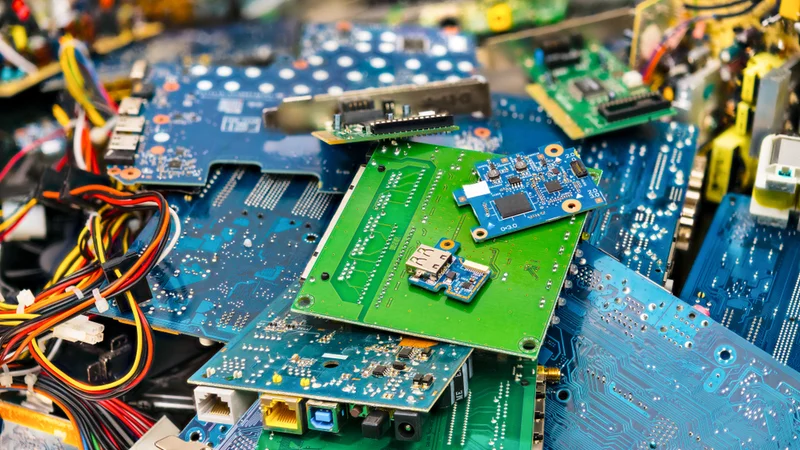
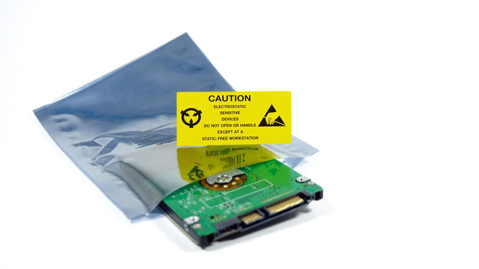
Printed circuit boards (PCBs) are the foundation of modern electronics, providing a reliable method of connecting electronic components. These boards consist of conductive tracks, pads, and other features etched from copper sheets laminated onto a non-conductive substrate, such as FR-4. PCBs are crucial in various applications, from consumer electronics to industrial equipment and aerospace systems. The different types of printed circuit boards, including single-sided, double-sided, and multi-layer boards, cater to specific design requirements and constraints.
Advanced PCB technologies, such as flexible, rigid-flex, and high-density interconnect (HDI) PCBs, have been developed to address the challenges of increasingly complex and compact electronic devices. Understanding the diverse types of printed circuit boards is instrumental in selecting the most suitable option for a particular application.
PCB Fundamentals
The basic structure of a printed circuit board (PCB) consists of a non-conductive substrate, typically made from materials such as FR-4, polyimide, or PTFE. Conductive copper traces, pads, and other features are etched onto the surface of the substrate to create the desired electrical connections.
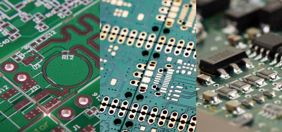
Copper traces electrically connect the various components mounted on the PCB. The current-carrying requirements and the desired impedance of the circuit determine the width and thickness of these traces.
Vias are the small holes drilled through the PCB and plated with conductive material, allowing for electrical connections between different board layers. Several types of vias, including through-hole, blind, and buried vias, each serving specific purposes in PCB design.
Solder masks, usually made from a polymer coating, are applied to the PCB surface to protect copper traces from oxidation and prevent short circuits during soldering. The solder mask also provides electrical insulation between adjacent traces and pads.
Key components and materials in PCB fabrication include:
Copper foil: Available in various weights (e.g., 0.5 oz, 1 oz, 2 oz), copper foil creates conductive traces, pads, and planes. [1]
Substrate materials: FR-4 is the most common base material, offering good mechanical and electrical properties, while polyimide and PTFE are used for high-frequency and high-temperature applications.
Solder mask: Liquid Photo-imageable (LPI) solder masks are widely used for their precision and durability.
Silkscreen: A printed layer that adds text, logos, and component identifiers to the PCB surface, aiding in assembly and troubleshooting.
Surface finishes: Coatings such as hot air solder leveling (HASL), electroless nickel immersion gold (ENIG), or organic solderability preservative (OSP) that protect exposed copper and enhance solderability.
PCB Materials and Their Properties
FR-4, a glass-reinforced epoxy laminate, is widely used in the PCB industry due to its balanced electrical, thermal, and mechanical properties. With a dielectric constant of 4.5 at 1 MHz and a dissipation factor of 0.02, FR-4 is suitable for general-purpose applications. [2] Its glass transition temperature (Tg) ranges from 130°C to 180°C, with a thermal conductivity of 0.3 W/mK.
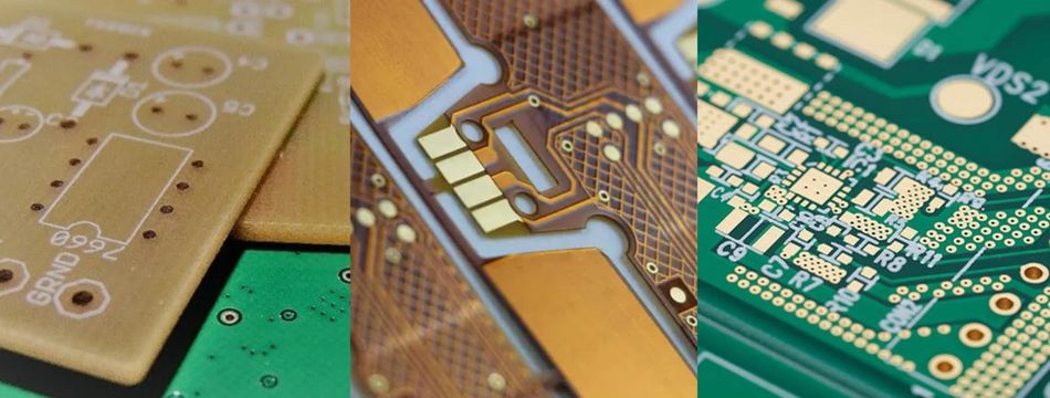
Polyimide, a high-performance polymer, offers excellent thermal stability, chemical resistance, and mechanical strength. Its dielectric constant of 3.2 to 3.6 at 1 MHz and dissipation factor of 0.002 make it suitable for high-frequency applications. Polyimide's glass transition temperature ranges from 260°C to 400°C, with a thermal conductivity of 0.2 W/mK. With high tensile strength (100-200 MPa) and flexural strength (200-400 MPa), polyimide is ideal for flexible and rigid-flex boards. [3]
PTFE (polytetrafluoroethylene), or Teflon, is a fluoropolymer with excellent dielectric properties, low dissipation factor, and high thermal stability. Its dielectric constant of 2.1 at 1 MHz and dissipation factor of 0.0002 make it an ideal choice for high-frequency and microwave applications. [4] PTFE has a melting point of 327°C and a thermal conductivity of 0.25 W/mK. However, its relatively low mechanical strength and high cost limit its use to specialized applications, such as radar systems and satellite communications.
When selecting metal core materials for a PCB, it is essential to consider the application's specific requirements, such as thermal performance, weight, and cost.
| PCB Material | Dielectric Constant at 1 MHz | Dissipation Factor | Thermal Conductivity (W/mK) | Flexural Strength (MPa) | Glass Transition Temperature (°C) |
| FR-4 | 4.5 | 0.02 | 0.3 | 400 - 800 | 130 - 180 |
| Polyimide | 3.5 | 0.002 | 0.2 | 200 - 400 | 260 - 400 |
| PTFE | 2.1 | 0.0002 | 0.25 | 10 - 20 | N/A |
PCB Design Considerations
Proper PCB design ensures optimal performance, reliability, and manufacturability in electronic devices. Designers must carefully consider various factors to create PCBs that meet the specific requirements of their applications.
Here are the top PCB design considerations:
Component placement: Optimize component placement for signal integrity, thermal management, and manufacturability. Consider the size, shape, orientation, and proximity of components to minimize interference and ensure proper functionality.
Signal integrity: Maintain signal quality and timing throughout the PCB by proper trace routing, impedance matching, and minimizing crosstalk and EMI. Use techniques such as ground planes, avoiding sharp bends, and proper termination to ensure signal integrity. Employ simulation tools and analysis techniques, such as TDR and eye diagrams, to optimize performance.
Thermal management: Manage heat dissipation to prevent component failure and ensure reliable operation. Consider electric component power dissipation, ambient temperature, and available cooling methods. Use thermal vias, copper pours, and heat sinks to dissipate heat effectively. Employ thermal simulation tools to analyze and optimize thermal performance, especially for high-power applications.
Power distribution: Design a robust power distribution network (PDN) to provide stable and clean power to all components. Properly size and place power and ground planes, minimize voltage drops and reduce power supply noise. Use decoupling capacitors and optimize via placement to improve power distribution.
Manufacturing constraints: Consider the limitations and capabilities of the PCB manufacturing process, including minimum trace width and spacing, hole sizes, and layer count. Design within these constraints to ensure reliable and cost-effective manufacturing.
Cost: Balance the cost of materials, components, and manufacturing processes with the desired performance and reliability. Make trade-offs between factors such as layer count, material selection, and component choices. Use standard sizes and minimize the number of unique components to reduce costs.
Electromagnetic compatibility (EMC): Ensure that the PCB does not generate excessive EMI and is not susceptible to external EMI. Employ techniques such as proper grounding, shielding, and filtering. Adhere to EMC standards and regulations, particularly in the automotive, aerospace, and medical industries.
Recommended Reading: PCB Material: A Comprehensive Guide to Understanding and Choosing the Right Materials
Types of PCBs
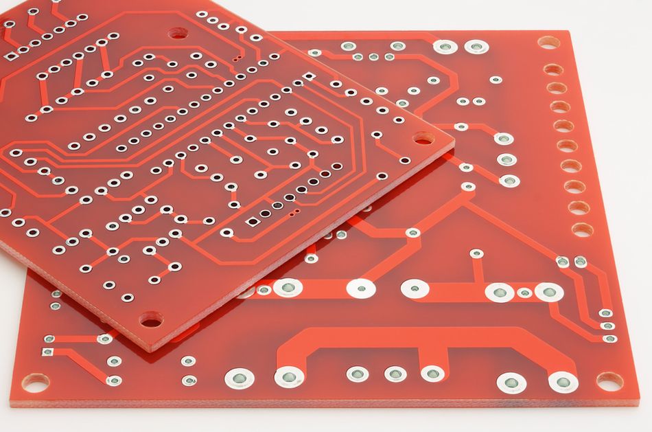
Understanding the differences between the main types of printed circuit boards (PCBs) is crucial for selecting the most suitable option for a given application. The three primary types of PCBs are single-sided, double-sided, and multi-layer boards, each with its characteristics, advantages, and limitations.
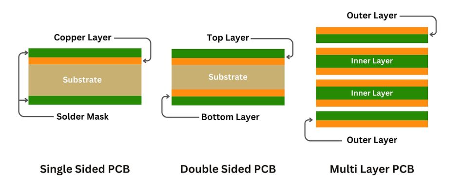
Single-sided PCBs feature conductive traces and components on only one substrate side, typically made of FR-4 material. These boards are the simplest and most cost-effective, ideal for low-complexity circuits, such as those found in basic electronic devices and prototypes. However, single-sided PCBs have limited routing options and lower component density, restricting their use in more advanced applications.
Double-sided PCBs have conductive traces and components on both sides of the substrate, connected using through-hole vias. These vias are drilled holes plated with conductive material, allowing electrical signals to pass between layers. Double-layer PCBs offer more complex routing and higher component density compared to single-sided boards, making them suitable for various applications, from consumer electronics to industrial control systems. The increased complexity of double-sided PCBs also allows for better signal integrity and improved thermal management.
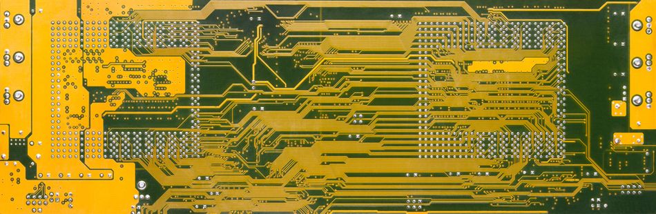
Multi-layer PCBs consist of three or more conductive layers, separated by insulating material or layers made of prepreg. These boards offer the highest level of complexity and component density, making them ideal for advanced applications such as high-speed digital circuits, RF systems, and aerospace electronics.
Multi-layer PCBs allow for intricate routing, better signal integrity, and improved thermal management, as the inner layers can be used for power and ground planes. The increased number of layers also enables the use of advanced techniques, such as blind and buried vias, which further enhance the capabilities of multi-layer PCBs. However, the increased complexity and manufacturing requirements of multi-layer PCBs are more expensive than single-sided and double-sided boards.
| Characteristic | Layers | Density | Complexity | Cost | Signal Integrity | Applications |
| Single-Sided PCBs | 1 | Low | Simple | Low | Low | Simple Devices |
| Double-Sided PCBs | 2 | Medium | Moderate | Medium | Medium | Consumer Electronics |
| Multi-Layer PCBs | 3 | High | High | High | High | High-Performance Systems |
Single-Sided PCBs
Single-sided PCBs are the simplest type of printed circuit board, consisting of a non-conductive substrate, typically made of FR-4 material, with conductive traces and components on only one side.
The manufacturing process involves applying a layer of copper foil to the substrate, which is then etched away to create the desired circuit pattern. This etching process is usually done using a photoresist method, where a light-sensitive polymer is applied to the copper foil, and a photomask with the circuit pattern is placed on top. The board is exposed to UV light, hardening the exposed photoresist. The unexposed photoresist is then removed using a developer solution, and the unprotected copper is etched away using an acidic solution, leaving only the desired circuit pattern.
Advantages of single-sided PCBs:
Low cost due to simple structure and manufacturing process
Quick turnaround time for faster design and manufacturing
Easy to modify for prototyping and low-volume production
Limitations of single-sided PCBs:
Limited routing options due to single conductive layer
Lower component density restricting use in advanced applications
Reduced signal integrity and increased EMI compared to double-sided or multi-layer PCBs
Single-layer PCBs find applications in various areas, such as:
Simple electronic devices (e.g., toys, calculators, low-cost consumer electronics)
Prototyping and testing new designs before moving to more complex PCB types
Educational purposes to teach students about electronic circuits and PCB design principles
Multi-Layer PCBs
Multi-layer PCBs consist of three or more conductive layers, separated by prepreg (pre-impregnated) insulating layers. The conductive layers are typically made of copper foil, and the insulating layers are bonded together using heat and pressure in a lamination process. The inner layers of a multi-layer PCB can be used for power and ground planes, while the outer layers are used for signal routing and component placement.
The manufacturing process for multi-layer PCBs is more complex than that of single-sided and double-sided boards. It involves the following steps:
The inner layers are patterned and etched using the photoresist method.
The etched inner layers are then laminated together with prepreg insulating layers using heat and pressure.
Through-holes are drilled through the laminated board and plated with copper to create vias that connect the layers.
The outer layers are then patterned and etched using the photoresist method.
A solder mask is applied to protect the copper traces, and a silkscreen layer is added for component labeling and identification.
Multi-layer PCBs offer several advantages over single-sided and double-sided boards:
They can accommodate a much higher number of components and complex circuitry in a smaller footprint.
The use of dedicated power and ground planes helps to reduce electromagnetic interference (EMI) and crosstalk, resulting in better signal integrity.
The additional layers can be used to dissipate heat more effectively, improving the thermal performance of the board.
Multi-layer PCBs allow for more complex routing and the use of advanced techniques, such as blind and buried vias, which enable more efficient and compact designs.
However, multi-layer PCBs also have some limitations:
The complex manufacturing process and additional materials required for multi-layer PCBs make them more expensive than single-sided and double-sided boards.
The increased complexity of multi-layer PCBs can result in longer design and manufacturing lead times compared to simpler board types.
The multiple layers and complex design of multi-layer PCBs make them more difficult to repair and modify compared to single-sided and double-sided boards.
Multi-layer PCBs are essential in a wide range of applications, such as:
High-speed digital devices: Multi-layer PCBs are crucial for high-speed digital devices, such as computers, servers, and networking equipment, where signal integrity and thermal management are critical.
Aerospace and defense systems: The high reliability, compact size, and advanced capabilities of multi-layer PCBs make them essential for aerospace and defense applications, such as avionics, radar systems, and satellite communications.
Medical equipment: Multi-layer PCBs are used in medical equipment, such as imaging systems and patient monitoring devices, where high performance, reliability, and miniaturization are required.
Recommended Reading: PCB Layers: Everything You Need to Know
Advanced PCB Technologies
Advanced PCB technologies, such as flexible PCBs, rigid-flex PCBs, and high-density interconnect (HDI) PCBs, are driving innovation in modern electronics by enabling the development of more compact, flexible, and high-performance devices. These technologies offer unique features and capabilities that push the boundaries of traditional PCB design and manufacturing.
Flexible PCBs, constructed from thin, flexible materials like polyimide or polyester, can bend and twist without damaging the conductive traces. This flexibility makes them ideal for applications requiring conformity to irregular shapes or resistance to vibration, such as wearable electronics, medical devices, and aerospace systems. The ability to bend and fold flexible PCBs allows for more compact and space-efficient designs in these applications.
Rigid-flex PCBs offer the best of both worlds by combining rigid and flexible substrates into a single board. The rigid sections provide structural support and accommodate components that require stability, while the flexible sections allow for bending and folding in specific areas. This unique combination enables the creation of three-dimensional designs and the integration of multiple circuit boards into a single assembly. Rigid-flex PCBs find applications in space-constrained devices like smartphones, laptops, and medical implants, where reliability and compact packaging are essential.
High-density interconnect (HDI) PCBs feature fine pitch traces, small vias, and high component density, making them crucial for the increasing miniaturization and functionality demands of modern electronics. HDI PCBs employ advanced manufacturing techniques, such as microvias (vias with diameters less than 150 microns) and buried vias (vias that do not extend to the outer layers of the board), to achieve higher routing density and improved signal integrity. These boards are indispensable in applications requiring high-speed data transfer, such as 5G networks, high-performance computing, and advanced driver assistance systems (ADAS) in vehicles.
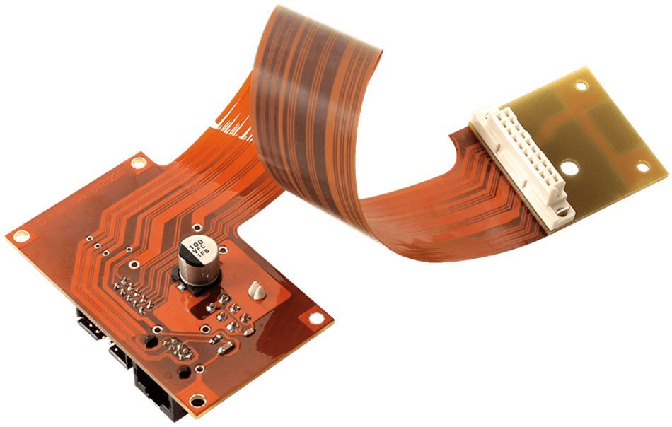
Flexible PCBs
Flexible PCBs, or flex circuits, are printed circuit boards made from thin, flexible materials such as polyimide or polyester. These materials allow the board to bend and twist without damaging the conductive traces, making them ideal for applications requiring flexibility or limited space. The conductive traces on flexible PCBs are typically made of copper, which is bonded to the flexible substrate using adhesives.

The manufacturing process for flexible PCBs involves:
Printing conductive traces onto the flexible substrate using screen printing or photolithography
Etching the traces using a chemical process to remove unwanted copper
Laminating additional layers of flexible substrate and conductive traces, if required
Cutting the final circuit to the desired shape using a die-cutting process
Advantages of flexible PCBs:
Flexibility for applications requiring bending or conformity to specific shapes
Space savings through folding or rolling up, enabling more compact designs
Weight reduction due to thin, lightweight materials
Durability and resistance to vibration and shock
Limitations of flexible PCBs:
Limited component options compared to rigid boards
Higher cost due to materials and manufacturing processes
Reduced heat dissipation due to lower thermal conductivity of thin, flexible materials
Flexible PCBs find applications in various fields, such as:
Wearable devices (e.g., smartwatches, fitness trackers, medical monitoring devices)
Compact electronics (e.g., smartphones, tablets, laptops)
Automotive electronics (e.g., instrument clusters, infotainment systems, sensors)
Rigid-Flex PCBs
Rigid-flex PCBs are a combination of rigid and flexible PCBs, integrating both types of substrates into a single board. The rigid sections, made from standard FR-4 material, provide structural support and accommodate components that require stability. The flexible sections, made from thin, flexible materials such as polyimide, allow for bending and folding in specific areas and are typically used to connect the rigid sections, creating a three-dimensional PCB assembly.
The manufacturing process for rigid-flex PCBs involves:
Preparing the rigid and flexible substrates separately, creating conductive traces and vias using standard PCB manufacturing techniques
Applying adhesive to the rigid and flexible substrates in the areas where they will be joined
Aligning and laminating the substrates together using heat and pressure to create a single, integrated board
Performing additional drilling and plating processes to create electrical connections between the rigid and flexible sections
Cutting and shaping the final board to the desired form factor
Advantages of rigid-flex PCBs:
Increased reliability by eliminating connectors between rigid and flexible sections
Space savings through three-dimensional packaging and reduced need for separate connectors and cables
Improved signal integrity due to the integrated nature of rigid-flex PCBs
Enhanced durability, as flexible sections can withstand repeated bending and flexing
Limitations of rigid-flex PCBs:
Higher costs due to complex manufacturing processes and specialized materials
Increased design complexity, requiring careful consideration of mechanical and electrical properties of both rigid and flexible sections
Limited flexibility compared to purely flexible PCBs, with potential limitations in bend radius and number of flex cycles
Rigid-flex PCBs are preferred in applications where reliability, space savings, and durability are critical, such as:
Aerospace and defense (e.g., avionics, satellites, military equipment)
Medical devices (e.g., implantable devices, surgical instruments, diagnostic equipment)
Wearable electronics (e.g., smartwatches, fitness trackers)
Automotive electronics (e.g., engine control modules, infotainment systems)
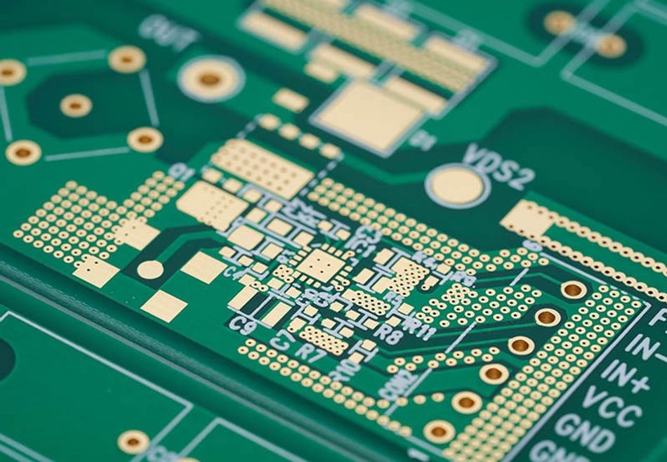
High-Density Interconnect (HDI) PCBs
High-Density Interconnect (HDI) PCBs are characterized by their fine pitch traces, small vias, and high component density. These features enable HDI PCBs to accommodate the increasing miniaturization and functionality demands of modern electronics. HDI PCBs typically have trace widths and spacings of 100 microns or less, and via diameters of 150 microns or less. [5] They often incorporate microvias, which are vias with diameters less than 150 microns, and buried vias, which do not extend to the outer layers of the board.
The manufacturing process for HDI PCBs involves several advanced techniques:
The PCB is built up layer by layer, with each layer being laminated and drilled separately. This allows for the creation of fine pitch traces and microvias.
Microvias are drilled using high-precision laser systems, enabling the creation of small, accurate holes.
After drilling, the microvias are filled with copper using an electroplating process to create reliable electrical connections between layers.
HDI PCBs often use staggered via patterns to maximize space utilization and minimize signal interference.
HDI PCBs offer several advantages over traditional PCBs:
The fine pitch traces and small vias allow for a higher density of components on the board, enabling more compact and functional designs.
The shorter signal paths and reduced layer count in HDI PCBs lead to improved signal integrity and reduced noise and crosstalk.
The increased copper content in HDI PCBs, due to the high density of traces and vias, helps to dissipate heat more effectively.
The compact nature of HDI PCBs allows for smaller and lighter electronic devices.
However, HDI PCBs also have some limitations:
The advanced manufacturing processes and materials used in HDI PCBs result in higher costs compared to traditional PCBs.
Designing HDI PCBs requires specialized knowledge and tools to ensure proper signal integrity, thermal management, and manufacturability.
The high density and small features of HDI PCBs make them more difficult to repair and rework compared to traditional PCBs.
HDI PCBs are essential in a wide range of applications that require high performance, compact size, and advanced functionality, such as:
Smartphones: HDI PCBs are crucial in enabling the compact size, high performance, and rich features of modern mobile phones.
High-performance computing: HDI PCBs are used in servers, workstations, and other high-performance computing systems to enable fast data transfer and processing.
Wearable devices: The compact size and high functionality enabled by HDI PCBs make them ideal for use in wearable devices, such as smartwatches and fitness trackers.
Medical devices: HDI PCBs are used in advanced medical devices, such as implantable devices and diagnostic equipment, where high reliability and compact size are essential.
Recommended Reading: Mastering QFN Packages: A Complete Guide to Compact and High-Performance Electronics Encapsulation
Signal Integrity and EMI Considerations
Signal integrity refers to a signal's ability to maintain its quality and timing as it propagates through the PCB, while EMI is the unwanted electromagnetic energy that can interfere with the proper functioning of electronic components. [6] Addressing these issues is essential for preventing signal distortion, crosstalk, and electromagnetic compatibility problems.

Maintaining signal integrity in PCB board design involves:
Impedance matching: Matching the impedance of the signal path to the source and load impedance
Trace routing: Optimizing trace routing to minimize crosstalk, reflections, and delay skew
Termination: Using appropriate termination techniques to minimize signal reflections and ringing
Grounding and power distribution: Designing a robust ground plane and power distribution network
Minimizing EMI in PCB design involves:
Shielding: Using shielding materials to contain electromagnetic emissions
Grounding: Implementing proper grounding techniques to minimize ground loops and provide a low-impedance path for EMI currents
Filtering: Using filters to suppress high-frequency noise and prevent EMI propagation
Trace routing: Routing high-speed signals away from sensitive components and using differential signaling
Examples of techniques used to address signal integrity and EMI issues:
Microstrip and stripline: Controlled impedance trace geometries for maintaining signal integrity and minimizing crosstalk and EMI
Via stitching: Adding vias along ground plane edges to provide a low-impedance path for high-frequency currents
Guard traces: Placing grounded traces alongside sensitive signals for shielding and crosstalk reduction
Decoupling capacitors: Using decoupling capacitors near IC power pins to suppress high-frequency noise
Spread-spectrum clocking: Employing spread-spectrum clock generation to reduce peak electromagnetic emissions at specific frequencies
PCB Manufacturing Challenges and Considerations
PCB manufacturing involves numerous challenges and considerations to ensure the production of high-quality, reliable, and cost-effective boards. Addressing these issues is crucial for maintaining a competitive edge in the electronics industry.
Here are the top challenges and considerations in PCB manufacturing:
Component sourcing:
Managing lead times, minimum order quantities (MOQs), and component obsolescence
Ensuring quality and authenticity of components to avoid reliability issues and product failures
Design for manufacturability (DFM):
Considering factors such as component placement, trace routing, and soldermask design
Collaborating with designers to identify and resolve potential manufacturability issues early in the design process
Process control:
Monitoring and controlling key process parameters (e.g., etching times, plating thicknesses, reflow profiles)
Implementing statistical process control (SPC) techniques to identify and correct process deviations
Quality assurance:
Conducting incoming inspection of components, in-process testing, and final functional testing
Maintaining detailed traceability records to enable rapid identification and containment of quality issues
Environmental regulations:
Managing the use of hazardous substances and implementing environmentally friendly manufacturing processes
Properly handling and disposing of waste materials to minimize environmental impact
Rapid technological advancements:
Investing in new equipment and processes to support the production of advanced technologies (e.g., HDI, flexible circuits)
Continuously training the workforce to maintain the skills and knowledge required to produce advanced products
Cost pressures:
Optimizing manufacturing processes to minimize waste and improve efficiency
Implementing cost-reduction initiatives (e.g., lean manufacturing, automation) and managing the supply chain for best pricing without compromising quality
Recommended Reading: The Printed Circuit Board Design and Manufacturing Cycle: Symbiotic Relationships Engage Innovation
Conclusion
This article has provided an in-depth overview of different types of PCBs and their applications in the electronics industry. The advanced PCB technologies offer unique features and capabilities, enabling the development of more compact, flexible, and high-performance electronic devices. Looking ahead, PCB technology is expected to continue advancing to meet the ever-increasing demands for miniaturization, high-speed performance, and enhanced functionality in electronic devices.
Some of the key trends shaping the future of PCBs include the adoption of advanced materials, such as graphene and carbon nanotubes, the integration of embedded components, and the development of 3D printing techniques for PCB fabrication. These advancements have the potential to revolutionize the electronics industry, enabling the creation of more innovative, efficient, and sustainable electronic products.
Frequently Asked Questions (FAQs)
Q. What is the difference between a single-sided and a double-sided PCB?
A. A single-sided PCB has conductive traces and components on only one side of the substrate, while a double-sided PCB has conductive traces and components on both sides of the substrate. Double-sided PCBs offer more routing options and higher component density compared to single-sided PCBs.
Q. What are the advantages of using multi-layer PCBs?
A. Multi-layer PCBs offer several advantages, including higher component density, improved signal integrity, enhanced thermal management, and increased design flexibility. They enable the creation of more complex and compact electronic devices.
Q. When should I consider using a flexible PCB?
A. Flexible PCBs are ideal for applications that require flexibility, such as wearable devices, medical equipment, and aerospace systems. They are also useful in situations where space is limited, and the PCB needs to conform to a specific shape.
Q. What is the purpose of using HDI PCBs?
A. HDI (High-Density Interconnect) PCBs are used in applications that require high component density, improved signal integrity, and reduced size and weight. They are essential in devices such as cell phones, tablets, and high-performance computing systems.
Q. How does thermal management affect PCB performance?
A. Proper thermal management is crucial for ensuring the optimal performance and reliability of electronic devices. It helps to dissipate heat generated by components, preventing overheating and potential component failure. Techniques such as using thermal vias, heat sinks, and selecting appropriate PCB materials can help improve thermal management.
Q. What are some of the challenges faced in PCB manufacturing?
A. PCB manufacturing faces several challenges, including component sourcing, design for manufacturability (DFM), process control, quality assurance, environmental regulations, rapid technological advancements, and cost pressures. Addressing these challenges is essential for producing high-quality, reliable, and cost-effective PCBs.
Q. What are the future trends in PCB technology?
A. Future trends in PCB technology include the adoption of advanced materials (e.g., graphene, carbon nanotubes), the integration of embedded components, and the development of 3D printing techniques for PCB board fabrication. These advancements aim to enable the creation of more innovative, efficient, and sustainable electronic products.
References
[1] JHDPCB. Thick Copper PCB / Heavy Copper PCB [Cited 2024 April 18] Available at: Link
[2] Wevolver. PCB Material: A Comprehensive Guide to Understanding and Choosing the Right Materials [Cited 2024 April 18] Available at: Link
[3] ReversePCB. Polyimide Rigid PCB: The Strongest Material for Your PCB Project [Cited 2024 April 18] Available at: Link
[4] Microwaves101. PTFE [Cited 2024 April 18] Available at: Link
[5] Copperdot. HDI PCBs — High-density Interconnect Printed Circuit Boards [Cited 2024 April 18] Available at: Link
[6] Cadence. Signal Integrity Fundamentals in PCB Layout [Cited 2024 April 18] Available at: Link