Flexible PCBs in Modern Engineering
This article delves into the innovative world of flexible printed circuit boards, uncovering their design, advancements, and transformative role in modern engineering applications.

02 May, 2024. 11 minutes read
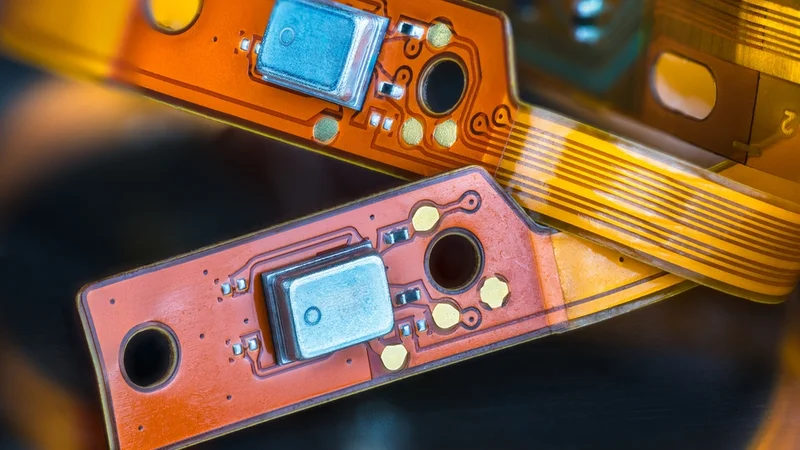
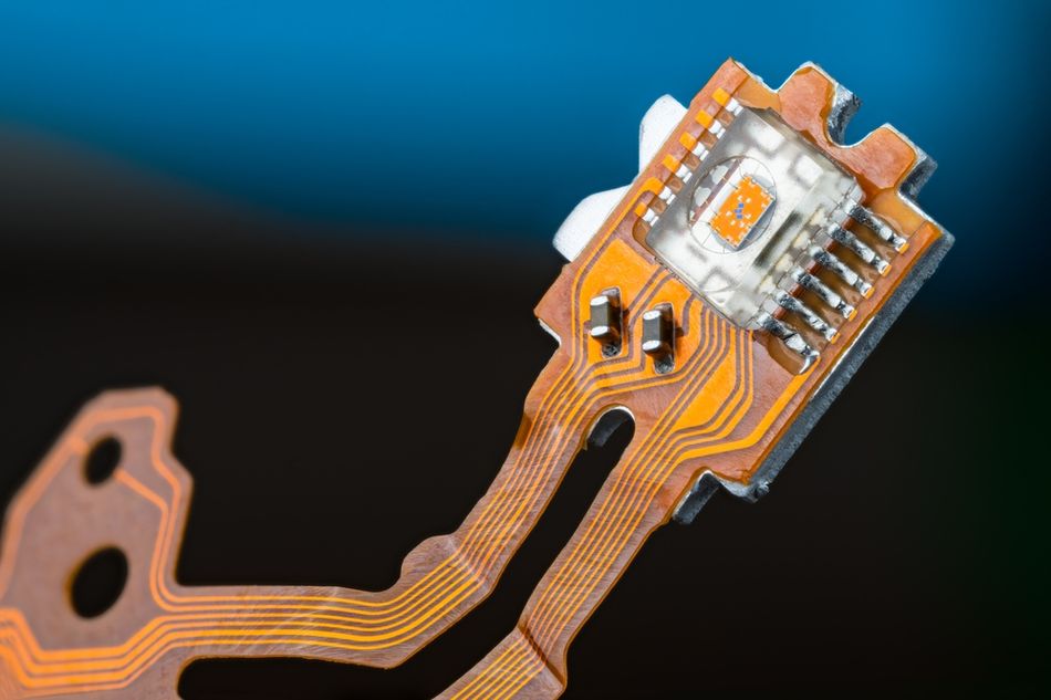
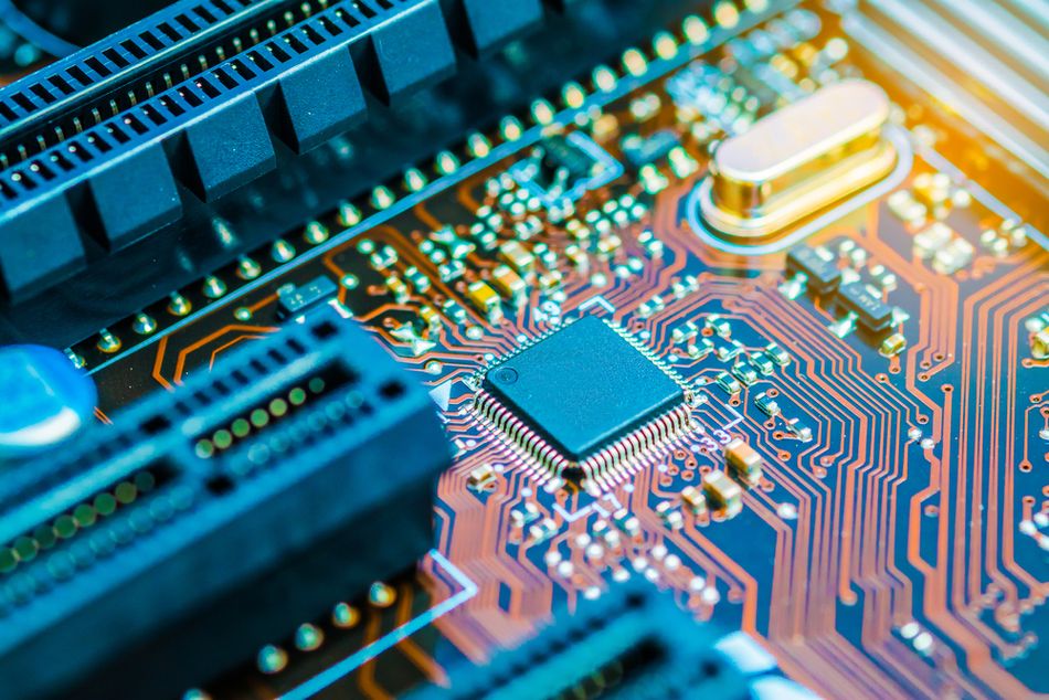
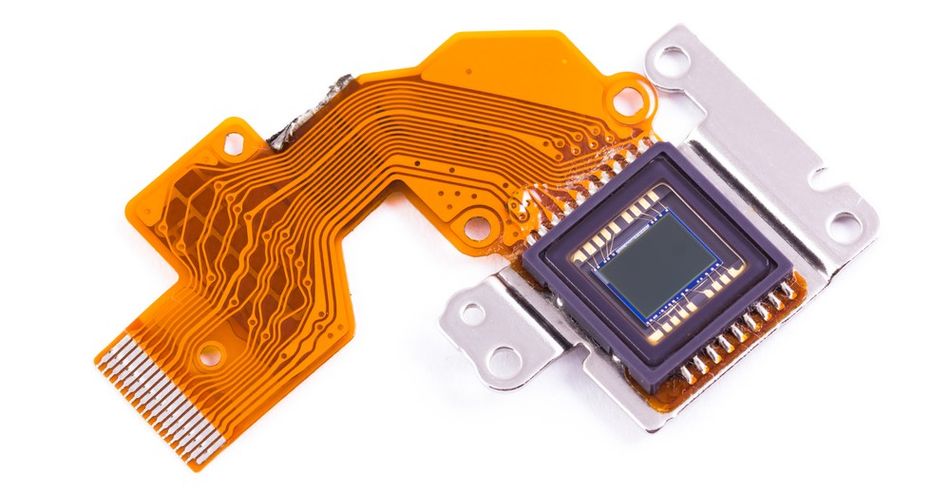
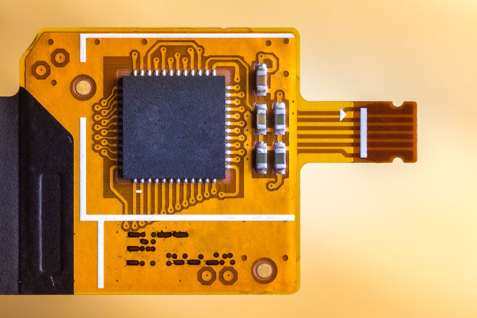
PCB or small components on flexible ribbon cables
Introduction
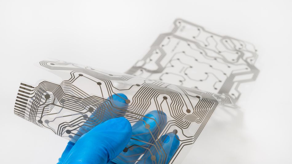
Flexible printed circuit boards (PCBs) have revolutionized electronic circuit design with their ability to conform to various shapes and spaces, unlike traditional rigid-flex PCBs. Flexible PCBs are made from materials like polyimide or polyester film, allowing them to withstand repeated bending without losing their structural integrity. This flexibility makes them ideal for compact and robust electronic designs, as the copper traces etched onto these substrates maintain conductivity even when bent.
Their distinct properties have made flexible PCBs a critical component in the miniaturization of electronics. As portable and wearable devices proliferate, flexible PCBs meet the market's demand for lightweight and space-efficient technology. They are integral to the innovation in fields ranging from medical devices to consumer electronics, driving the industry forward with new possibilities in electronic component integration. Let’s start with understanding the anatomy of flexibility!
Unfolding the Layers: Understanding Flexible PCBs
The Anatomy of Flexibility
Flexible PCBs are the circuit boards that can bend and flex without breaking and losing their functionality. They are made of a thin layer of plastic substrate, such as polyimide, polyester film, or polyethylene terephthalate (PET), with copper circuits laminated on one or both sides. [1] These substrates support flexibility and offer significant thermal stability and durability under operational stresses.
Key electrical properties of these materials include:
Dielectric Constants (Dk): This property determines the speed at which electrical signals travel through the FPC. Flexible printed circuit materials, like polyimide, typically have a lower Dk compared to FR4, the material used in rigid-flex circuits, which allows for faster signal transmission. The dielectric constant of the base material also affects the impedance of an FPC.
Loss Tangent (Df): This value represents the amount of energy lost as heat when a signal travels through the FPC. A lower Df indicates lower signal loss and better signal integrity. FPCs generally have lower Df values than rigid PCBs, making them suitable for high-frequency applications.
Conductivity: The electrical conductivity of the copper traces in an FPC determines their ability to carry current. FPC manufacturers use high-conductivity copper to minimize signal loss and ensure efficient current flow.
Thermal Stability: The ability to withstand high temperatures enhances the reliability of flexible circuit boards during both manufacturing and end-use.
Tensile Strength: Despite their flexibility, the materials are robust, resisting mechanical stresses such as stretching and tearing during manufacturing and usage.
Flexibility: The core characteristic that allows these PCBs to be used in innovative electronic board designs without damage when bent or folded.
Materials commonly employed in the construction of flexible PCBs are:
Polyimide (PI): Noted for its excellent thermal stability and chemical resistance.
Polyester (PET): Provides a cost-effective balance of performance and flexibility.
Liquid Crystal Polymer (LCP): Selected for its superior frequency performance and low moisture absorption.
Polyethylene Naphthalate (PEN): Valued for its heat resistance and dimensional stability.
Each material is chosen based on how its specific properties align with the intended application, impacting everything from the PCB's durability to its electrical performance.
Layers of Flexible PCBs (FPCs)
Similar to rigid PCBs, FPCs consist of multiple layers laminated together. However, due to their flexibility, the materials and construction differ slightly. Stack-up refers to the arrangement of layers in a PCB, including the base material, conductive layers, and dielectric layers. [2]
Here's a breakdown of the typical layers in an FPC:
Topcoat: The topcoat is a protective layer applied to the FPC's outer surface. It protects the underlying layers from scratches, abrasions, and chemicals.
Coverlay: The coverlay is a dielectric material layer, applied on top of the copper layers. It is basically an insulator, that protects the circuits from electrical shorts.
Copper Circuits: The copper circuits are the conductive layers or pathways that carry electrical signals. They are typically made of etched copper foil.
Adhesive: The adhesive is a single layer of material that bonds the copper circuits to the substrate.
Substrate: The substrate is the base layer of the FPC. It is typically made of a thin, flexible plastic material such as polyimide or PET.
Bottom Layer (optional): Some FPCs have copper circuitry on the bottom and top sides.
Depending on the design, there can be some additional layers:
Stiffeners: In some FPC designs, particularly those with high component density or requiring more rigid sections, stiffener layers might be incorporated. These are typically made of FR4, strategically placed on specific areas to provide additional support and prevent excessive bending.
Soldermask: A protective layer applied over the copper traces, except for designated soldering areas. It prevents unwanted solder bridges and shorts during component assembly.
The number of layers in an FPC directly impacts its flexibility, complexity, and cost. Designers strive to minimize layer count for optimal flexibility and cost-effectiveness while achieving the desired functionality.
Recommended Reading: Rigid Flex PCB: Revolutionizing Modern Electronics Design
FPC Design Principles and Manufacturing Process
Designing flexible circuit boards requires careful consideration to ensure they can bend and flex without compromising electrical integrity or functionality. Key factors include material selection and circuit path layout to prevent stress points that could lead to failure. Since FPCs bend and flex, their design requires careful consideration compared to rigid boards.
Here are some key principles to follow:
Minimize Layer Count: Multilayer FPCs offer more functionality but are more complex and expensive to manufacture. It is better to aim for single-sided or double-sided designs whenever possible.
Bend Radius: FPCs have a minimum bend radius below which they can permanently deform or break. The design should consider the FPC's intended bending requirements and stay above this limit.
Component Selection: Components chosen for FPC applications should be lightweight and surface-mount technology (SMT) compatible for easy assembly on the flexible substrate.
Trace Width and Spacing: FPC traces are thinner and more prone to damage than those on rigid PCBs. Designers must maintain adequate width and spacing to prevent electrical shorts and maintain current carrying capacity.
Vias and Holes: Via density should be minimized due to the complexity of via formation in FPCs. Large or high-density via fields might require thicker substrates or special techniques, impacting flexibility.
Tear Points and Slots: Strategically placed slots or perforations can be incorporated into the design to allow controlled bending without damaging the circuit traces.
The manufacturing process for flexible PCBs differs significantly from that of rigid PCBs and includes the following steps:
Material Selection: The appropriate base material (polyimide or PET), copper foil thickness, and adhesive are chosen based on the application's demands.
Circuit Design: Using software to design circuits, carefully planning flex areas to minimize stress.
Photolithography: Applying a photosensitive material to the substrate and exposing it through a mask to define the circuit pattern.
Etching: The unwanted copper is removed from the foil using chemical etching, leaving behind the designed circuit traces.
Drilling (optional): Holes (vias) are drilled through the substrate for electrical connection between layers in multilayer FPCs.
Plating (optional): Vias are metalized through an electroless plating to establish electrical connections between layers. Flexible circuit boards can have plated through holes (PTHs), but they are less common than rigid PCBs because they can add complexity and reduce flexibility.
Lamination: Coverlayers and stiffeners (if needed) are bonded to the base film with copper traces using heat and pressure. Adhesiveless lamination is used to create FPCs that are thinner and more flexible.
Surface Finish: The FPC surface is metalized with a desired finish, such as ENIG or OSP, for improved solderability and corrosion resistance.
Testing: Electrical testing is conducted to ensure the FPC functionality under simulated real-world flexing conditions.
Die Cutting: The final FPC shapes are precisely cut out from the larger panel. Laser cutting is a common method for cutting out the final shapes of FPCs from a larger panel.
Inspection and Packaging: The completed FPCs undergo final inspection and are carefully packaged for shipment.
Innovations like laser direct imaging (LDI), roll-to-roll (RTR) lamination and conductive inks have refined flexible PCB manufacturing. [3] LDI enhances trace patterning accuracy, essential for dense circuit designs, while conductive inks facilitate circuit creation in highly bendable areas. Roll-to-Roll (RTR) lamination allows for the efficient processing of multiple FPC layers simultaneously, improving production speed.
Challenges primarily involve layer alignment and bonding in multi-layer flex circuits. Precise alignment during lamination is critical to prevent circuit failure, necessitating specialized equipment and techniques to ensure layer registration.
Innovations in Flex Circuit Technology
Pioneering Materials and Techniques
Flexible PCB technology is advancing rapidly with the adoption of new materials that offer superior performance. Graphene stands out for its excellent electrical and thermal conductivity, coupled with remarkable mechanical flexibility. This two-dimensional material is revolutionizing flexible circuit boards, enabling thinner, lighter, and more efficient designs.
Conductive polymers are transforming the landscape of flexible electronics with their inherent flexibility and processability at lower temperatures. These materials are particularly suited for wearable devices and medical applications, where they harmonize electronic functionality with the human body.
Advanced composites are another frontier in flexible PCB materials. These composites deliver enhanced thermal stability and mechanical resilience by combining materials like ceramics or nano-fillers with traditional substrates. They are tailored for specific applications, addressing the demanding requirements of modern electronics.
Integrating these pioneering materials into flexible PCBs improves their performance and unlocks new possibilities in electronics design, enabling innovations from foldable displays to advanced sensors.
The Rise of Stretchable Electronics
Stretchable PCBs represent a significant advancement over traditional flexible PCBs by offering the ability to elongate and adapt to dynamic surfaces without damage. This capability is crucial for applications requiring electronics to conform to non-static, variable shapes, such as wearable devices that integrate seamlessly with the human body.
The innovative use of elastomeric substrates and liquid metal conductors is at the core of stretchable electronics. Elastomeric substrates, typically silicone-based, provide the necessary flexibility and resilience, while liquid metal conductors, such as gallium alloys, ensure continuous electrical conductivity even when stretched. [4]
The engineering of stretchable electronics involves overcoming challenges related to maintaining circuit functionality during and after deformation. Design strategies often include creating serpentine or meandering conductive paths that can expand and contract effectively without losing electrical integrity. The field is rapidly evolving, with ongoing research to enhance the durability and performance of these circuits under mechanical stress.
Flexible Printed Circuit (FPC) interconnects, and connectors have been developed to meet the challenges of this expanding market, which demands smaller centerline or pitch spacing, lower profile heights, and lighter interconnect solutions. FPCs are also used to create HDI circuits and replace wire harnesses for compact and lighter-weight flex circuit boards.
Applications of stretchable electronics are diverse and growing, ranging from smart textiles that monitor health metrics to components in soft robotics that require electronics to flex with the robot’s movements. These applications highlight the potential of stretchable PCBs to revolutionize how electronics are used in daily life and specialized environments.
Recommended Reading: Understanding PCB Thickness: A Comprehensive Guide
Engineering Applications: Flex PCBs in Action
Revolutionizing Consumer Electronics
Flexible PCBs are revolutionizing consumer electronics by enabling more compact, innovative designs. In smartphones, their flexibility facilitates the development of foldable screens, which combine large display areas with portability. Wearables like fitness trackers and smartwatches benefit from flexible PCBs, which conform to ergonomic designs for enhanced comfort and functionality.
A notable case study involves a leading smartphone manufacturer that integrated flexible PCBs into a foldable phone. This innovation allowed for a dual-screen device that remains compact when folded, offering users a large display that fits comfortably in their pockets. Another example is a fitness tracker that features a curved display optimized for the wrist's contour, made possible by flexible PCBs. This design improves the device's ergonomics and user interface.
FPCs are used in automotive applications such as airbags, instrument clusters, and navigation systems because they resist vibration and shock. [5] These examples underscore the critical role of flexible PCBs in advancing consumer electronics and other applications, enabling devices that are more functional, user-friendly, and aesthetically pleasing.
Flex PCBs in Medical Devices
Flexible PCBs have become essential in medical devices, offering adaptability and resilience critical for patient care. Their application ranges from life-sustaining implants like pacemakers to wearable monitors that track vital signs with precision and comfort.

The compact nature of flexible PCBs enables less invasive implantable electronic devices, conforming to anatomical structures and minimizing patient discomfort. Wearables benefit from the thin, lightweight profile of flexible PCBs, allowing for continuous health monitoring without impeding daily activities.
The advantages of flexible PCBs in medical devices are multifaceted. They provide enhanced patient comfort, more accurate data collection, and greater reliability in diverse medical environments. The intimate contact these PCBs can maintain with the skin is vital for sensors tasked with capturing critical health metrics.
Biocompatibility is paramount in medical applications, necessitating materials that are non-reactive and safe for long-term contact with biological tissues. Sterilization compatibility is equally important, ensuring that devices can be safely used without compromising their electronic integrity.
Regulatory compliance, particularly with FDA standards, is rigorous for medical devices incorporating flexible PCBs. This ensures that every device meets the highest safety and performance criteria before reaching the healthcare market.
Recommended Reading: PCBA Design Trends to Watch in 2023
Navigating the Challenges of Flex PCBs
Reliability and Durability Concerns
Flexible PCBs face significant reliability and durability challenges due to their inherent flexibility. This flexibility, while advantageous for fitting into unconventional shapes, also makes the PCBs susceptible to wear and fatigue at bend points.
To mitigate these issues, advanced materials and design strategies are employed. These include using materials that distribute stress more evenly and applying protective coatings to shield against environmental factors such as moisture and heat. Some FPCs can be conformally coated, making them resistant to liquids immersion.
The balance between flexibility and durability is crucial. Enhancing flexibility often involves using thinner materials, which may reduce the PCB's overall durability. Engineers must carefully design these PCBs to ensure they meet the application's demands without compromising longevity.
Reliability testing is integral to the development of flexible PCBs. Tests include flex endurance testing to simulate repeated bending, thermal cycling to assess temperature resilience, and moisture resistance testing. These evaluations help pinpoint potential failure modes and refine the PCB design to address them.
A case study in wearable technology illustrates these principles in action. A flexible PCB designed for a high-durability wearable underwent rigorous flex endurance testing, which revealed critical stress points. The subsequent redesign incorporated a tougher substrate and optimized component placement, significantly enhancing the product's reliability and demonstrating the value of comprehensive testing and adaptive design.
Recommended Reading: Unfolding the Future: The Evolution and Impact of Printed Electronics
Conclusion
Flexible PCB technology has significantly reshaped the landscape of modern engineering, introducing a level of versatility and innovation previously unattainable with traditional rigid PCBs. The ability of these circuits to bend, fold, and flex opens up new dimensions in product design across various industries, from consumer electronics to medical devices.
The transformative potential of flexible PCBs lies in their capacity to integrate into compact and complex device configurations, enabling the development of more portable, lightweight, and sophisticated products. Ongoing research and development are crucial as they drive advancements in materials and manufacturing processes, further expanding the capabilities and applications of flexible PCBs. This continuous innovation ensures that flexible PCB technology remains at the forefront of the electronics industry, pushing the boundaries of what's possible in engineering design.
Frequently Asked Questions
Q. What are the main advantages of using flexible PCBs?
A. Flexible PCBs offer significant advantages, including reduced space and weight, which are essential for modern, compact devices. They also improve reliability by withstanding harsh environments and mechanical stresses better than rigid PCBs. Additionally, their dynamic flexing allows for greater design freedom, enabling engineers to create more innovative and functional designs.
Q. How do flexible PCBs impact the design and functionality of consumer electronics?
A. Flexible PCBs have revolutionized the design and functionality of consumer electronics by facilitating the miniaturization of devices while enhancing their versatility. Their ability to conform to different shapes and sizes allows for innovative product designs such as foldable smartphones and wearable technology, making electronics more adaptable to user needs.
Q. What are the challenges in flex PCB manufacturing?
A. Manufacturing flexible PCBs presents both technical and economic challenges. Technically, ensuring durability and maintaining performance while the PCB flexes requires precise material selection and circuit design. Economically, the assembly costs of flexible PCBs can be higher due to the specialized materials and processes involved, posing challenges in scaling production while managing costs.
References
[1] ResearchGate. Polymer Substrates for Flexible Electronics: Achievements and Challenges [Cited 2024 April 29] Available at: Link
[2] Wevolver. PCB Layers: Everything You Need to Know [Cited 2024 April 29] Available at: Link
[3] Sierra Circuits. Laser Direct Imaging system accurately images PCB panels [Cited 2024 April 29] Available at: Link
[4] ResearchGate. Directed Assembly of Liquid Metal–Elastomer Conductors for Stretchable and Self‐Healing Electronics [Cited 2024 April 29] Available at: Link
[5] JLCPCB. The Role of Flex PCBs in Automotive Electronics [Cited 2024 April 29] Available at: Link
in this article
1. Introduction2. Unfolding the Layers: Understanding Flexible PCBs3. FPC Design Principles and Manufacturing Process4. Innovations in Flex Circuit Technology5. Engineering Applications: Flex PCBs in Action6. Navigating the Challenges of Flex PCBs7. Conclusion8. Frequently Asked Questions9. References