How Does a Zener Diode Work? Theory, Operation & Practical Applications
Zener diodes are unique semiconductor devices designed to operate in reverse bias and maintain a stable voltage. This article explains how a Zener diode works, from its quantum-tunneling breakdown mechanism to practical uses in voltage regulation and circuit protection.

23 Jul, 2025. 12 minutes read
Key Takeaways
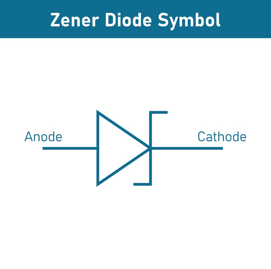
A Zener diode is a specially doped PN-junction diode designed to reliably conduct current in reverse once the voltage across it reaches a specified breakdown threshold, known as the Zener voltage.
Under reverse bias, a Zener diode blocks current until the reverse voltage reaches its Zener breakdown voltage (Vz), causing a controlled breakdown and allowing current to flow while maintaining a nearly constant voltage at Vz.
Zener breakdown is driven by quantum tunneling in heavily doped junctions and dominates at lower voltages (Vz<≈5−6 V), while avalanche breakdown, caused by impact ionization in lightly doped junctions, dominates at higher voltages.
By operating in its steep breakdown region, a Zener diode maintains a nearly constant voltage across itself, making it ideal for creating simple voltage regulators when placed in shunt with a load and a series resistor.
Zener diodes are widely used for voltage regulation, creating stable reference voltages, overvoltage protection, waveform clipping, and as noise sources in random number generators.
Introduction
Imagine you need to derive a stable 5 V supply from a fluctuating higher-voltage source in a pinch, or protect a sensitive circuit from voltage spikes. A tiny component called the Zener diode can do just that. Zener diodes are a staple in electronic design, acting as simple shunt regulators and reference sources in countless circuits. They are named after physicist Clarence Zener, who first described the electrical breakdown phenomenon in 1934.
In essence, a Zener diode is a silicon diode engineered to operate in reverse bias at a well-defined voltage. When the reverse voltage across it exceeds a certain threshold (the Zener voltage VZ), the diode enters breakdown and conducts current, but crucially maintains a nearly constant voltage drop equal to VZ. This behavior makes Zener diodes invaluable for voltage regulation and overvoltage protection. In this article, we’ll explore how a Zener diode works at the physics level and how to apply it in practical circuits.
What is a Zener Diode?
A Zener diode is a heavily doped PN-junction diode designed to conduct in reverse once a specific reverse-bias voltage is reached. In normal operation (forward-bias), it behaves like an ordinary diode, with a forward voltage around 0.7 V for silicon. However, when reverse-biased, a Zener diode will block current like a typical diode only up to a point.
As soon as the reverse voltage equals the device’s breakdown voltage (the Zener voltage VZ, sometimes called the knee voltage), the diode’s junction breaks down and it starts conducting in reverse. Unlike an ordinary diode that would be damaged by breakdown, the Zener diode is built to withstand this reverse breakdown safely and maintain a stable voltage across itself during conduction.
Zener diodes are characterized by their Zener breakdown voltage VZ, which is set during manufacturing by controlling the doping level of the silicon. Thanks to precise doping techniques, the breakdown voltage can be tailored to a desired value and held within tight tolerances (commonly 5% or 10%, with specialized parts available at <1% tolerance).
Standard Zener diodes are available with VZ as low as ~2 V (even ~1.2 V in some cases) and as high as 200 V or more. They also come with various power ratings (from tiny 0.25 W or 0.5 W diodes for low currents, up to several watts for power applications) – exceeding the power limit causes overheating.
Suggested Reading: Diode Symbols: A Comprehensive Guide to Understanding Circuit Diagrams
How Does a Zener Diode Work?
The zener diode primarily works in reverse bias once the voltage is high enough. To understand this, let’s contrast its behavior in forward vs. reverse bias and then delve into the two types of breakdown that allow reverse conduction.
Forward Bias (Low Voltage)
When a Zener diode’s anode is made more positive than its cathode (forward-bias), it behaves like a typical silicon diode. It has a forward voltage drop of about 0.7 V (for silicon) at nominal current, and current flows freely above that forward threshold.
Reverse Bias (Pre-Breakdown)
When the diode is reverse-biased (cathode positive relative to anode) and the voltage is below the breakdown point, only a very small leakage current (microampere-scale) flows, as with any diode’s reverse saturation current. The diode essentially looks like an open circuit in this region.
Reverse Bias (Breakdown Region)
As the reverse voltage increases to the device’s engineered breakdown threshold (Vz), suddenly, the diode’s PN junction undergoes electrical breakdown. At this Zener voltage, a dramatic increase in reverse current occurs with only a minor further increase in voltage.
The diode effectively clamps the voltage across itself to approximately VZ, conducting whatever current is necessary (limited by the surrounding circuit) to maintain that voltage. This is a controlled breakdown – the diode is designed to enter this region without damage as long as the current is limited.
Suggested Reading: Forward Bias, Reverse Bias and their effects on Diodes
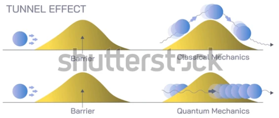
Zener Breakdown (Quantum Tunneling Effect)
The reason Zener diodes achieve breakdown at low voltages is heavy doping of the semiconductor. It creates a phenomenon called the Zener effect. Heavy doping of the P and N regions yields a very thin depletion region at the junction, on the order of micrometers or less. When the diode is reverse-biased, an extremely strong electric field builds across this thin depletion layer (on the order of 3×10⁵ V/cm, or ~500 kV/m) even at relatively low voltages. Such a strong field can directly pull electrons from their valence bonds in the semiconductor lattice, yanking them into the conduction band.
In quantum terms, electrons tunnel through the narrow energy barrier from the valence band of the p-side to the conduction band of the n-side. This tunneling current marks the onset of Zener breakdown. It is essentially a quantum mechanical effect – the electric field enables charge carriers to tunnel through the bandgap.
Zener breakdown is dominant in low-voltage Zener diodes, typically those with a Vz of about 5 V or less. In this regime, the breakdown happens at a well-defined voltage, and the I–V curve in breakdown is relatively soft (rounded) compared to a sharp snap-off, meaning the voltage increases a little as current increases.
Avalanche Breakdown Mechanism
For Zener diodes with higher breakdown voltages, a different mechanism takes over, called the avalanche breakdown. Avalanche breakdown is a classic mechanism also seen in ordinary diodes or other semiconductor junctions when a large reverse bias is applied.
In a lightly doped PN junction (with a wider depletion region), the electric field under reverse bias is not initially strong enough to cause tunneling. Instead, as the reverse voltage increases, charge carriers (minority carriers that are thermally generated) are accelerated by the electric field across the depletion region to high speeds.
These high-energy electrons (or holes) can collide with the lattice atoms and knock loose additional electrons, generating new electron-hole pairs. Those freed carriers are likewise accelerated and can free even more carriers in a chain reaction. This cascading effect leads to a sudden surge in reverse current – the avalanche.
Avalanche breakdown typically occurs at higher reverse voltages (commonly Zener diodes above ~6 V use avalanche as the dominant effect). It has a positive temperature coefficient, meaning the breakdown voltage increases with temperature (opposite to the Zener effect). Avalanche breakdown usually has a sharper knee in the I–V curve – once the voltage reaches the avalanche point, current rises very steeply.
I–V Characteristics of a Zener Diode
The current–voltage (I–V) characteristic of a Zener diode captures its behavior in forward and reverse operation. In the forward region, the curve looks just like a typical diode – a forward turn-on around 0.7 V for silicon, beyond which current rises rapidly.
The reverse region is more interesting: initially, as reverse voltage increases, only a tiny leakage current flows. This continues until the voltage approaches the breakdown knee. At the breakdown voltage Vz, the current begins to increase sharply with almost no further increase in voltage. In the breakdown region, the I–V curve is nearly vertical, indicating the diode will conduct a large change in current for a very small change in voltage, effectively clamping the voltage around Vz.
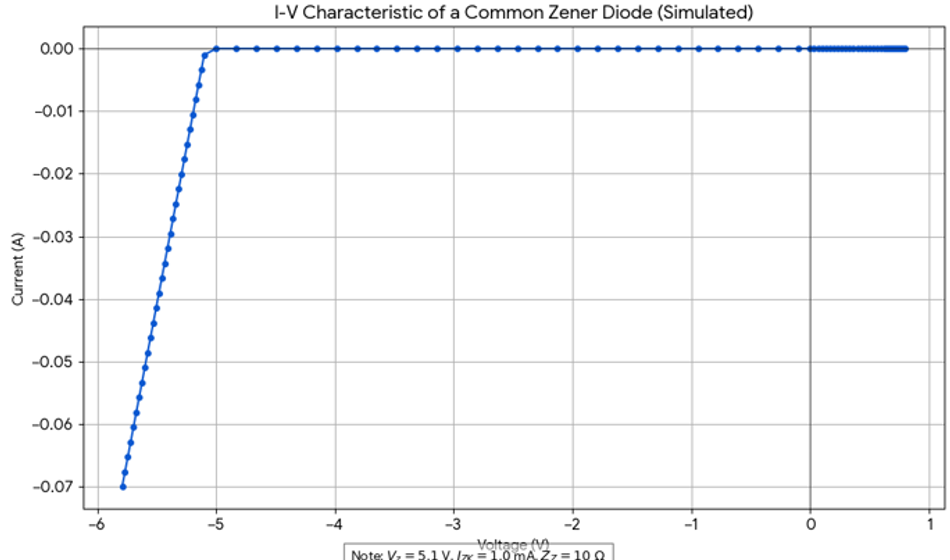
For a Zener diode to regulate voltage properly, it must be biased such that it stays in the breakdown (regulation) region. This means a current at or above a certain minimum knee current Iz(min) must flow. Below this current, the diode might drop less than Vz and fall out of regulation. On the other hand, there is also a maximum current, Iz(max), set by the diode’s power dissipation limit.
Exceeding this risks overheating. The region between Iz(min) and Iz(max) is the usable range where the diode maintains roughly constant voltage. Within this range, the diode has a small slope in its V–I curve due to its internal dynamic resistance (rz).
Zener Diode Specifications
While picking a Zener diode for electronics circuits, designers must consider the key parameters which include:
Parameter | Description | Typical Values/Notes |
Nominal Zener Voltage (VZ) | The specified breakdown voltage at which the Zener diode operates in reverse bias. | Ranges from roughly 2 V to 200 V or more. Measured at a specified test current (IZt). Common series: BZX55/BZX85, 1N47xx. |
Tolerance on VZ | The permissible variation from the nominal Zener voltage. | E.g., ±5%. Finely set by doping during manufacturing. |
Maximum Power Dissipation (Pmax) | The maximum power the diode can safely dissipate without damage. | E.g., 500 mW, 1 W, etc. Can be used to estimate maximum current (IZM=Pmax/VZ). |
Dynamic Resistance (ZZ) | The AC resistance of the Zener diode in its breakdown region indicating how much VZ changes with IZ. | Measured at the operating point. Higher for high-voltage (avalanche) Zeners (>≈50 V). Lower values indicate better voltage regulation. |
Test Current (IZt) | The specific current at which the nominal Zener voltage (VZ) is measured and specified in the datasheet. | Often a few mA for low-power Zeners. Crucial for accurate VZ specification. |
Maximum Current (IZM) | The highest current the Zener diode can safely conduct in reverse bias without exceeding its power rating. | It can be estimated as Pmax/VZ. Datasheets provide specific values. |
Temperature Coefficient | How the Zener voltage changes with temperature. | High-voltage Zeners (>≈50 V) typically have higher temperature coefficients. Mid-voltage Zeners (around 5−6 V) are very stable over temperature. |
Breakdown Mechanism | The physical effect causes the reverse breakdown. | Zener effect (quantum tunneling, heavily doped) dominates at lower voltages (VZ<≈5−6 V). Avalanche breakdown (impact ionization, lightly doped) dominates at higher voltages. |
Recommended Reading: Zener Diode: A Comprehensive Guide to Its Principles and Applications
Zener Diode as a Voltage Regulator
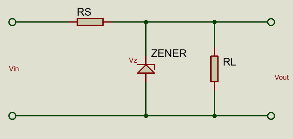
One of the most common uses of a Zener diode is as a shunt voltage regulator or reference. In this configuration, the Zener diode is reverse-biased across the output of a supply (or across a load) and holds the voltage at its breakdown value.
The simplest Zener regulator circuit consists of a Zener diode and a series resistor (often called a ballast or drop resistor) connected to a higher supply voltage.
For example, if you need to regulate approximately 5 V from a 12 V supply, you could use a 5.1 V Zener diode: connect the Zener in reverse bias from output to ground (cathode to the output node, anode to ground), then place a resistor from the 12 V input to the output node. When the output tries to rise above ~5.1 V, the Zener conducts and shunts excess current to ground, holding the voltage at ~5.1 V.
Suggested Reading: Optimizing Diode Functionality: Forward and Reverse Bias
According to Ohm’s Law, the current through the series resistor is:
Iz = (Vin - Vz) / Rs
- Minimum Current: The current through the Zener must stay above IZ(min) (the knee current) at maximum load. In other words, even under the heaviest load (which draws current away from the Zener), there should still be enough current flowing through the Zener to keep it in breakdown. If the current falls below this, the Zener will drop out of regulation, and the output voltage will sag below Vz.
- Maximum Current: The current through the Zener must stay below Iz(max) to avoid overheating. With no load (or light load), the Zener conducts the full current. This current times, Vz is the power dissipated in the diode. Exceeding Zener’s power rating will overheat and damage it. Thus, the series resistor should be large enough that even in the no-load case, the Zener current does not exceed the diode’s safe value.
Use Cases and Limitations
Zener regulators are simple and great for low-current applications or providing a reference voltage. For instance, they are often used to provide a reference to the base of a transistor in a more complex regulated power supply, or to power a small sensor or circuit that needs a stable lower voltage.
However, they waste energy as the difference between input and regulated voltage is dropped as heat in the resistor and Zener.
Suggested Reading: How Does a Diode Work: Unraveling the Heart of Electronic Control
Other Applications of Zener Diodes
Beyond basic voltage regulation, Zener diodes find use in a variety of protective and wave-shaping circuit roles. Here are a few common applications for Zeners in electronics design:
Surge and Overvoltage Protection
Zener diodes protect sensitive circuits from overvoltage by shunting excess current. When a voltage spike exceeds the Zener voltage (Vz), the diode conducts, clamping the circuit voltage to VZ and dissipating the surge energy.
This acts as a safety valve, preventing damage to components like microcontrollers. High-power Zeners, often called TVS diodes, are designed for absorbing large transients and ESD, characterized by their joule ratings to ensure they can handle the surge energy.
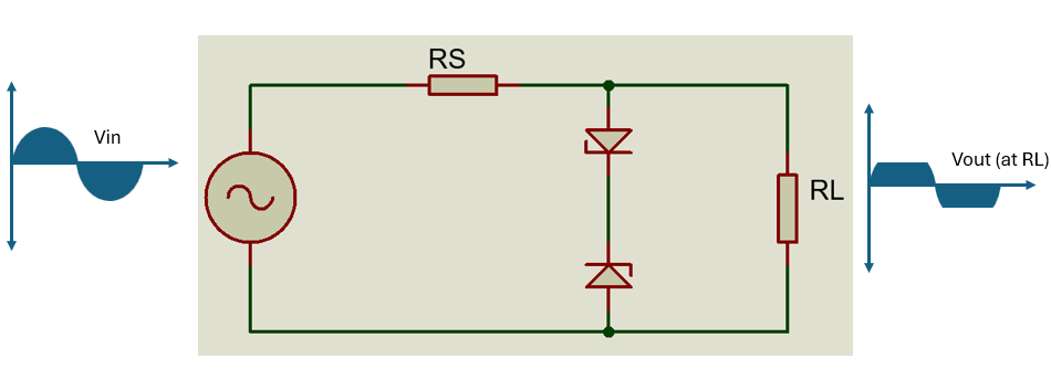
Signal Clipping and Waveform Shaping
Back-to-back Zener diodes are used to clip or limit signal waveforms. This configuration symmetrically clamps the signal peaks to approximately ±(Vz +0.7 V), where 0.7 V is the forward voltage drop of the opposing diode.
This prevents excessive voltage swings, shapes waveforms (e.g., approximating square waves from sine waves), and quickly protects circuit inputs from overvoltage, useful in audio limiters or amplifier input protection.
Voltage Reference and Level Shifting
Zener diodes can shift voltage levels by providing a fixed voltage drop. In series, they act as crude voltage droppers, but must handle the full load current. More commonly, they function as level shifters by clamping signals to their Zener voltage, protecting lower-voltage inputs (e.g., from a 12 V pulse to a 5.1 V microcontroller input), or creating fixed offsets in bias networks.
Noise Generation
Zener diodes in avalanche breakdown generate white noise due to random carrier collisions. This inherent noise is exploited in test equipment and for cryptographic random number generation, often amplified to create wideband noise sources. Avalanche Zeners, particularly 6−10 V types, are commonly used for this application.
Conclusion
Zener diodes are essential electronic components known for their ability to maintain a precise voltage in reverse bias. This controlled breakdown, whether through quantum tunneling (Zener effect) or avalanche multiplication, allows them to regulate voltage by shunting excess current. This unique characteristic makes them invaluable for applications such as creating stable voltage references, performing simple voltage regulation in shunt configurations, and protecting sensitive circuits from damaging voltage spikes.
Despite their versatility and low cost, Zener diodes have limitations. As regulators, they dissipate power as heat, making them less efficient for high-current applications. While suitable for many tasks, their voltage accuracy and temperature stability may not meet the demands of highly precise voltage reference ICs. However, the fundamental Zener principle continues to be integrated into advanced components like programmable shunt regulators and robust transient voltage suppressors, ensuring the discrete Zener diode remains a foundational element for reliable electronic designs.
FAQs
What is the difference between a Zener diode and a regular diode?
A Zener diode is designed for controlled, non-destructive conduction in reverse bias at a specific Zener voltage (VZ), unlike a regular diode which primarily conducts in forward bias and is typically damaged by reverse breakdown.
How does a Zener diode regulate voltage in a circuit?
In a shunt regulator, a reverse-bias Zener diode, with a series resistor, clamps the output voltage to its VZ. It achieves regulation by conducting more or less current to maintain a stable voltage despite input or load variations.
What are Zener diode breakdown voltage values available, and how do I choose one?
Zener voltages range from ≈2 V to 200 V (e.g., 5.1 V, 12 V). Choose a VZ matching your target voltage or protection threshold, considering its tolerance and datasheet-specified test current for accuracy.
Why do I need a resistor with a Zener diode?
A series resistor is crucial to limit the current flowing through the Zener diode when it's in breakdown. Without it, excessive current would flow, damaging the diode and potentially other circuit components.
Can Zener diodes be used to protect against high-voltage spikes (surges)?
Yes, Zener diodes, especially high-power TVS (Transient Voltage Suppressor) diodes, are commonly used for surge protection by clamping transient voltages to their VZ and shunting excess energy away from sensitive circuitry.
How does temperature affect Zener diode behavior?
Zener voltage (VZ) changes with temperature; low-voltage Zeners (<5 V) typically have a negative temperature coefficient (VZ decreases with temperature), while higher-voltage Zeners (>6 V) have a positive coefficient. Zeners around 5.6 V exhibit near-zero temperature sensitivity.
Can I use a Zener diode to get a higher voltage by putting them in series?
Yes, connecting Zener diodes in series sums their breakdown voltages, allowing for custom or higher voltage references; however, ensure adequate current limiting and consider combined tolerances and temperature coefficients.
References
[1] "The Zener Diode," Electronics Tutorials, n.d. [Online]. Available: https://www.electronics-tutorials.ws/diode/diode_7.html.
[2] "Zener Diode Voltage Regulator," Wira Electrical, n.d. [Online]. Available: https://wiraelectrical.com/zener-diode-voltage-regulator/.
[3] "What is a Zener Diode and How Does it Work?," CircuitBread, n.d. [Online]. Available: https://www.circuitbread.com/tutorials/what-is-a-zener-diode-and-how-does-it-work.
[4] S. A. Abbasi, "Zener Diode – Symbol, Working, Applications & Characteristics," Electrical Technology, May 2, 2022. [Online]. Available: https://www.electricaltechnology.org/2022/05/zener-diode.html.
[5] "Avalanche Diode," Electrical4U, n.d. [Online]. Available: https://www.electrical4u.com/avalanche-diode/.
[6] "Zener Breakdown and Avalanche Breakdown," CircuitGlobe, n.d. [Online]. Available: https://circuitglobe.com/zener-breakdown-and-avalanche-breakdown.html.
[7] "Diode vs Zener Diode," Electro University, n.d. [Online]. Available: https://electrouniversity.com/diode-vs-zener-diode/.