How Do MOSFETs Work: Comprehensive Technical Guide for Engineers (2025)
How do MOSFETs work? This article provides an in-depth exploration of their internal structure, electrical characteristics, operation modes, real-world use cases, and the latest technological advancements and trends for 2025!

07 Jul, 2025. 21 minutes read
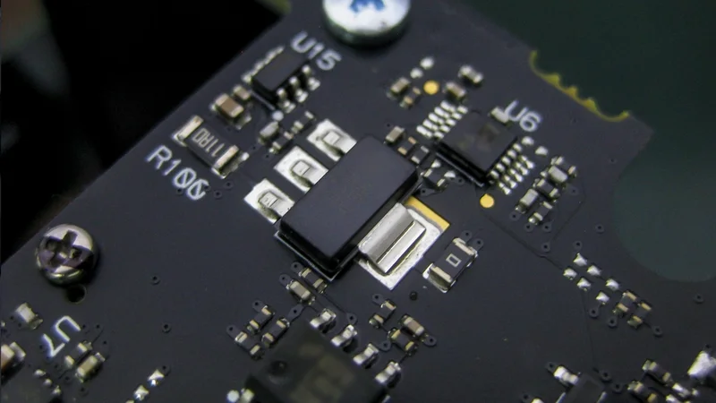
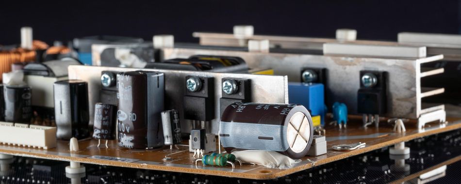
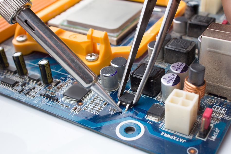
Transistor MOSFET on the Motherboard
Introduction
In modern electronics, the Metal-Oxide-Semiconductor Field-Effect Transistor (MOSFET) plays a vital role in enabling efficient switching and amplification. From power supplies and motor controllers to microprocessors and embedded systems, MOSFETs are foundational to countless applications. Understanding how do MOSFETs work is therefore essential for any engineer involved in electronic design.
This article offers an in-depth examination of their internal structure, electrical characteristics, operational modes, and real-world applications. If you're designing high-speed digital circuits or high-voltage power electronics, a deep understanding of how do MOSFETs work will equip you with the insight needed to innovate and troubleshoot with precision!
Theoretical Foundations Reveal How MOSFETs Work
MOSFET (Metal-Oxide-Semiconductor Field-Effect Transistor) is a voltage-controlled transistor at its core. It has four terminals – Gate (G), Drain (D), Source (S), and Body (substrate) – though in most circuits, the body is tied to the source. The structure of a MOSFET consists of a source and drain doped with one type of semiconductor (n+ or p+). This is separated by a body region of the opposite type, with a metal gate electrode insulated from the body by a thin oxide layer.
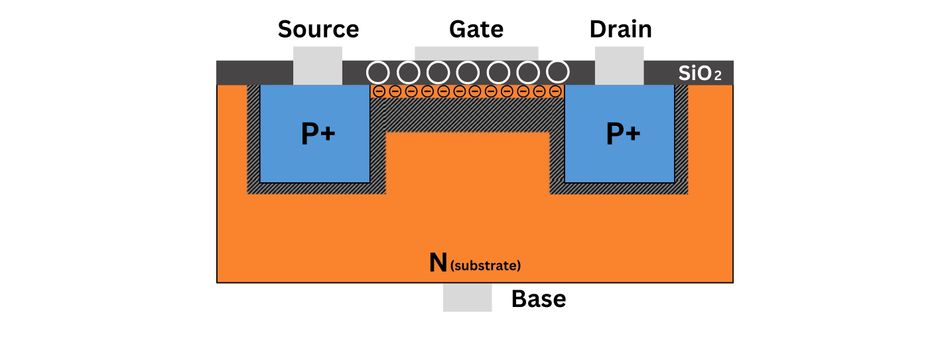
Structurally, an n-type or p-type silicon substrate forms the base! The source and drain regions are heavily doped with the opposite polarity type (e.g., n+ in a p-type substrate for n-channel MOSFETs). [1] The gate terminal is separated from the channel region by a thin oxide layer—commonly silicon dioxide—creating a high-input impedance insulated structure known as an insulated gate. The gate electrode, often made of polysilicon or metal, acts as one plate of a capacitor, with the oxide acting as the dielectric and the channel region underneath as the other plate.
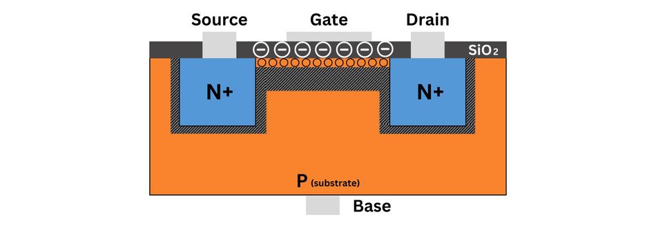
By applying a voltage between the gate and source (VGS), we create an electric field through the oxide layer that forms or disrupts a conductive channel in the body. This gate-to-body capacitance modulates charge carriers, allowing or blocking drain current (ID) between source and drain:
When VGS is below the threshold voltage (Vth), no conductive path forms—only a tiny leakage current may flow.
When VGS exceeds Vth, an inversion layer forms: electrons in NMOS or holes in PMOS, allowing current to pass.
Increasing VGS enhances the channel and reduces its resistance, increasing ID for a given drain-source voltage (VDS).
Recommended Reading: PMOS vs NMOS: Unraveling the Differences in Transistor Technology
Modes of Operation
MOSFET can operate in cutoff, linear (ohmic), or saturation regions depending on VGS, VDS, and Vth. For an enhancement-mode n-channel device:
If VGS < Vth, the transistor is in cutoff (off); only a tiny subthreshold leakage current flows.
If VGS > Vth and VDS is low, the MOSFET is in the ohmic region (acting like a voltage-controlled resistor). The channel is formed and ID increases approximately linearly with VDS.
If VGS > Vth and VDS is high enough that the channel “pinch off” occurs near the drain, and the MOSFET enters saturation (active region). In saturation, ID is relatively independent of VDS and is controlled primarily by VGS. A classic first-order model for saturation current is:
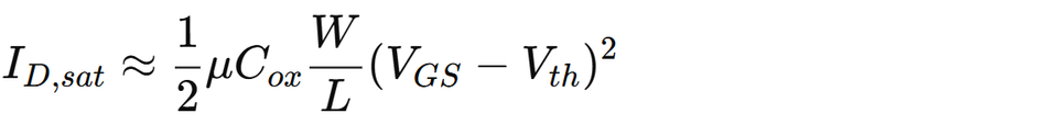
where μ is carrier mobility, Cox is gate oxide capacitance per area, and W/L is transistor width-to-length ratio.
This quadratic ID–VGS relationship shows that a higher gate voltage over threshold yields substantially more current (until real-world effects kick in). Modern MOSFET devices, especially at nanometer scales, deviate from the simple quadratic law due to channel length modulation, velocity saturation, etc., but the fundamental concept holds: the gate voltage modulates the channel charge and thus the current flow.
Types of MOSFET
MOSFETs come in two polarities and modes:
n-channel enhancement-mode MOSFET (the most common type) is off at VGS=0 and requires a positive VGS to turn on (for an nMOS, positive voltage in gate attracts electrons).
p-channel enhancement-mode MOSFET is complementary – it turns on with negative VGS (gate acquires more negative voltage than source attracts holes) and is off at VGS=0.
Depletion-mode MOSFETs which are normally on at zero gate bias and require reverse bias to turn off, but these are less common in modern digital circuits.
Most logic uses enhancement-mode devices (normally off, for fail-safe behavior). Additionally, MOSFET symbols and notations often show an intrinsic body diode (from body to the drain/source junction) – this body diode is an important parasitic element we’ll discuss later.
Recommended Reading: N-Type Vs P-Type: Difference Between P-Type and N-Type Semiconductors
Design Techniques Leverage Threshold Modulation
One of the most critical parameters in MOSFET operation is the threshold voltage (Vth)—the gate-to-source voltage (VGS) at which a conductive channel begins to form.
Engineers often use threshold modulation techniques to meet specific design goals such as reducing power consumption, enhancing speed, or managing thermal performance.
Multi Threshold CMOS (MTCMOS)
In modern semiconductor design, multi-threshold CMOS (MTCMOS) is a widely adopted technique. Foundries provide MOSFETs with different Vth values on the same die. Low-Vth devices are used in high-speed paths like clock buffers because they switch faster—requiring a smaller VGS to form a channel. However, they suffer from higher subthreshold leakage, especially in standby modes. In contrast, high-Vth transistors switch more slowly but leak far less current, making them suitable for memory blocks and idle logic.
To implement this technique, designers mix low- and high-threshold devices depending on each circuit block’s performance or power needs. Microprocessor, for example, may use low-Vth MOSFETs in timing-critical paths and high-Vth MOSFETs in standby logic to minimize leakage.
Threshold Modulation
Threshold modulation can also be achieved dynamically using body biasing. Since the threshold is affected by the voltage difference between the substrate (body) and the source terminal, applying a forward or reverse bias alters Vth—a phenomenon known as the body effect. By forward-biasing the substrate, designers can lower Vth, increasing switching speed. Reverse-biasing does the opposite, raising Vth to suppress leakage. This is the foundation of adaptive body biasing techniques, which tune Vth based on workload.
At the fabrication level, multiple thresholds are achieved through ion implantation, varying oxide thicknesses, or using high-k dielectrics. Mask steps define different regions with desired threshold voltage profiles—providing the foundation for energy-efficient designs.
Dynamic Threshold MOSFET (DTMOS)
Dynamic threshold MOSFET (DTMOS) is another technique where the gate terminal and body are connected. As the gate voltage rises, the body gets forward-biased, lowering Vth and boosting drive current. This is especially useful in low-voltage analog or digital circuits where performance-per-watt is critical.
In analog design, threshold tuning helps achieve precise biasing in current sources, temperature compensation, or improving voltage swing in transmission gates. Lower Vth improves signal integrity by ensuring the MOSFET passes voltages close to the power supply rails.
In conclusion, threshold modulation—via design or process—adds flexibility, allowing MOSFETs to adapt across applications, outperforming fixed-threshold bipolar junction transistors in dynamic environments.
Recommended Reading: Concurrent-Mode CMOS Detector IC for Sub-Terahertz Imaging System
Common Applications Span from Computing to Power Control
MOSFETs are foundational components in today’s electronics—serving as the primary switch in digital circuits, power systems, and analog designs. Their versatility comes from a combination of favorable characteristics: high input impedance, fast switching, low conduction losses, and scalability of manufacturing. Let’s explore their role in major application domains:
1. Digital Computing
In microprocessors, memory, and logic devices, MOSFETs form the core of CMOS logic gates and memory cell arrays. Billions of transistors are integrated into modern SoCs. For instance, M3 Ultra by Apple integrates roughly 184 billion MOSFET transistors on a single 3 nm die. [2]

These semiconductor devices function as both digital on/off switches and analog components—such as in DRAM sense amplifiers and capacitive storage. The CMOS architecture, which combines n-channel and p-channel MOSFETs, consumes almost no static power, drawing current only during switching. This efficiency is why nearly all microprocessors, controllers, and RAM use MOSFET-based logic.
In this domain, how MOSFETs work is centered around speed, density, and energy efficiency. Devices operate at low VGS values—often below 1 V—and switch at GHz speeds. Design priorities focus on reducing leakage, scaling transistor length, and managing thermal output through techniques like threshold modulation.
2. Power Electronics and Motor Control
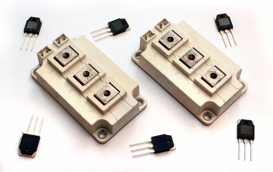
Discrete power MOSFETs are used in power supply units, DC-DC converters, and motor drivers at higher power levels. Their fast switching and low RDS(on) values make them ideal for controlling large currents with minimal heat loss.
For example, in automotive electronics, they control fuel injectors and drive inverters in EV battery systems. In consumer devices, they regulate voltage in laptop adapters, LED lighting, and portable chargers. Their low gate drive requirements eliminate the need for continuous input current, unlike bipolar junction transistors.
Power MOSFETs switch at high frequencies—often over 100 kHz—making them central to efficient switch-mode power supply design. Their low-loss switching also reduces the need for bulky resistors or large heatsinks, although high-current designs may still require thermal management.
Although MOSFETs typically max out around 900 V, IGBTs and SiC MOSFETs handle kilovolt ranges. Still, for mid-voltage ranges, power MOSFETs dominate due to their performance, ease of control, and integration flexibility.
3. Analog and RF Applications
In analog systems, MOSFETs act as voltage-controlled amplifiers. When biased in the saturation region, they function as transconductance devices, converting VGS into proportional drain current.
Applications include RF amplifiers, operational amplifiers, and mixed-signal ICs. For instance, LDMOS (Laterally Diffused MOSFETs) are widely used in mobile base station amplifiers due to their linearity, efficiency, and ability to deliver high RF output power.
In these designs, engineers utilize the input impedance, capacitance, and threshold voltage of MOSFETs to fine-tune signal gain and noise performance. They may operate as variable resistors in filters or as analog switches in sampling systems.
4. Specialty and Emerging Uses
MOSFETs also appear in sensor interfaces, ESD protection (every CMOS input has MOSFET-based protection networks), and even in MEMS and imaging (MOSFETs in CMOS image sensors act as pixel resets and amplifiers). The IGBT (Insulated Gate Bipolar Transistor), while not a pure MOSFET, uses a MOSFET gate structure to control a bipolar output section – blending MOSFET input ease with BJT-like output for very high power uses. This highlights how MOSFET technology even extends its influence into hybrid devices.
In summary, from nano-scale digital circuits to high-current motor control, understanding how MOSFETs work is essential. Their unmatched scalability, efficiency, and versatility ensure their role remains critical in nearly every electronic system in use today.
Recommended Reading: Selecting the Best Power Solution for Radio Frequency Signal Chain Phase Noise Performance
Integration with Gate Drivers Enables Fast Switching
Driving a MOSFET involves more than just applying voltage to the gate terminal—especially in power supply, high-frequency, or high-current systems. Because a MOSFET is a voltage-controlled device, its gate behaves like a capacitor. To switch effectively, that gate capacitance must be charged and discharged quickly. Without proper drive, the MOSFET may remain in partial conduction too long, increasing heat and switching losses.
That’s where a gate driver comes in! A gate driver is a circuit or IC designed to deliver the required gate-source voltage (VGS) and current to switch the MOSFET rapidly. For power MOSFETs, gate charge can be substantial—tens of nanocoulombs. If the gate is charged slowly (e.g., directly from a microcontroller output), switching may take microseconds, increasing energy loss during transitions. A dedicated gate driver can source or sink several amperes, charging the gate in nanoseconds, minimizing time spent in the high-loss linear region.
Consider a case where a gate requires 50 nC of charge! At 20 mA (from a typical MCU), this takes 2.5 µs. A gate driver delivering 2 A can do it in just 25 ns. This tenfold improvement dramatically reduces switching time, improving efficiency and lowering thermal stress.
Gate drivers also support level shifting, especially in high-side configurations of buck converters or half-bridges, where the gate needs to be driven above the supply rail. Advanced gate drivers use bootstrap capacitors, transformers, or capacitive coupling to enable this.
However, faster switching creates challenges too—high dV/dt and dI/dt can cause ringing, EMI, or voltage overshoot. To manage this, designers often insert a gate resistor (Rg) to control switching speed. This resistor shapes the gate current pulse and helps reduce unwanted transients.
For best performance, gate drivers must be physically close to the MOSFET gate, with short, low-inductance connections and a solid return path. Isolated paths for power and gate drive ground are also preferred to minimize common-mode noise.
In summary, fast, efficient switching requires dedicated gate drivers. They enable high-speed transitions, reduce energy loss, and improve circuit stability. Without them, the benefits of high-performance MOSFETs—like low on-resistance, fast response, and high-frequency operation—are compromised.
Modern Software Tools Revolutionize MOSFET Implementation
The development and optimization of MOSFET-based circuits have been transformed by powerful software tools. Where engineers once relied on hand calculations or basic simulators, today’s design process is led by advanced Electronic Design Automation (EDA) platforms. These tools model not only device-level physics but also full system behavior, including layout parasitics, thermal dynamics, and control loop interactions.
SPICE Simulation and Circuit Analysis
One of the most valuable tools is SPICE simulation (Simulation Program with Integrated Circuit Emphasis). Popular variants such as LTSpice, Spectre, and PSpice offer precise modeling of MOSFET behavior using manufacturer-provided data. These models incorporate key parameters such as threshold voltage, capacitance, drain current, body diode, and channel-length modulation.
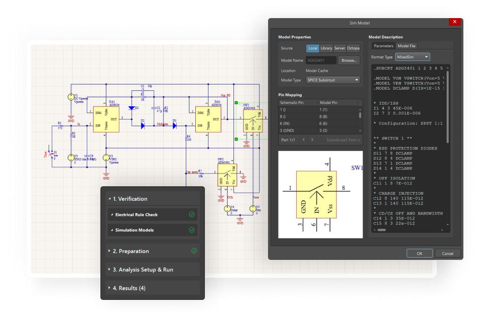
In SPICE, designers can build schematics using predefined MOSFET models, simulate switching behavior, and visualize time-domain responses. [3] Transient simulations help evaluate switching speed and overshoot, while DC sweeps extract I-V characteristics. AC analyses assist in optimizing small-signal gain or input impedance. These simulations help detect issues such as excessive power dissipation, slow transitions, or operation outside the safe operating area (SOA)—before hardware is even considered.
Specialized Tools for Power Electronics
Beyond SPICE, simulation platforms like PI Expert, MATLAB/Simulink, and Simscape provide system-level modeling of power supply circuits and converters. These allow engineers to simulate an entire buck or boost converter, including gate drivers, feedback control, and thermal effects.
Many MOSFET vendors also offer online calculators or model generators. By entering datasheet values, engineers can create custom SPICE subcircuits that match specific part characteristics. This enables precise modeling of power MOSFETs in switching regulators, battery chargers, and motor drivers.
PCB Layout and Thermal Co-Simulation
Design tools now include integrated thermal simulation and parasitic analysis, especially critical in power electronics where MOSFET performance is layout-dependent. Tools like Altium Designer and Cadence Allegro allow calculation of junction temperature, heat dissipation, and EMI based on layout geometry, copper area, and airflow.
More advanced tools enable electro-thermal co-simulation, showing how temperature rise from switching affects parameters like RDS(on) and Vth. This is vital for applications like high-density server power supplies, where MOSFETs operate near thermal limits.
IC Design and AI-Driven Optimization
For custom chips or ASICs, tools like Cadence Virtuoso and Synopsys Custom Compiler allow placing millions of MOSFETs, simulating at the transistor level, and automatically optimizing CMOS logic for speed and power. These platforms also support threshold modulation strategies, automatically selecting high-Vth or low-Vth devices depending on performance targets. The emerging AI-driven tools enhance this further by predicting MOSFET failures, suggesting optimal device choices, or generating control code for gate drivers in real-time.
Modern EDA tools have transformed MOSFET circuit design! Through simulation, thermal analysis, and intelligent modeling, engineers can ensure optimal performance, faster development, and greater reliability.
Recommended Reading: PCB Design: A Comprehensive Guide to Printed Circuit Board Design
Best Practices Address Common Implementation Pitfalls
Despite their versatility, MOSFETs require careful handling to avoid common mistakes. Improper gate control, poor thermal design, or flawed PCB layout can quickly lead to device failure.
Below are key best practices that help engineers fully realize the advantages of how MOSFETs work—reliably and efficiently.
1. Gate Drive and Biasing
The gate terminal should never be left floating! Noise can couple into the gate capacitance, unintentionally turning the device on. Always include a gate-to-source pull-down resistor (typically 100 kΩ) to ensure the gate discharges when inactive. When driven by microcontrollers, a series gate resistor (e.g., 50–100 Ω) protects the pin by limiting peak current and dampening EMI. Strong gate drivers benefit from gate resistors too, preventing overshoot and controlling rise/fall times.
2. Respect Voltage Ratings
Monitor VGS(max) and VDS(max) carefully. Applying excessive voltage—especially on logic-level MOSFETs—can damage the oxide layer. Use Zener diodes or clamps to protect the gate. On the drain side, design with a safety margin to accommodate voltage spikes from inductive loads. Ringing after turn-off may exceed the device’s breakdown voltage, risking avalanche failure unless the MOSFET supports it within its Safe Operating Area (SOA).
3. Thermal Management
MOSFETs generate heat through RDS(on) conduction and switching losses. Reference the thermal resistance specs in datasheet (junction-to-case and junction-to-ambient) and aim to stay well below the maximum junction temperature (usually 150°C–175°C). Use heatsinks, thermal vias, and large copper planes under the drain/source pads—especially with PowerPAK or DPAK packages. Remember: every 10°C increase in junction temperature can halve the device’s lifespan.
4. PCB Layout and Parasitics
High-speed switching converters demand tight PCB layout. Minimize the loop area between the power supply, MOSFET, diode (or synchronous MOSFET), and input/output capacitors. Long traces introduce parasitic inductance, resulting in overshoot (L × di/dt). Keep gate driver traces short. Place the gate resistor close to the gate pin. Use star grounding to isolate power and signal return paths. Watch out for the Miller effect—where dV/dt at the drain couples through Cgd and can cause unwanted gate turn-on. Miller clamps or RC snubbers can easily mitigate this.
5. Safe Operating Area (SOA)
Never assume a MOSFET can handle high current at any voltage. SOA charts show safe regions of operation. In linear mode or pulse loads, verify that the device won’t exceed thermal or electrical stress limits. Avoid using switching MOSFETs in analog pass applications unless rated for linear operation.
6. Body Diode Behavior
MOSFETs contain an intrinsic body diode, which can conduct during dead-time in H-bridge or inverter circuits. However, these diodes often have slow reverse recovery. To avoid excess losses, many designs use synchronous rectification—turning the MOSFET on instead of relying on its diode. If used, select MOSFETs with fast body diodes, and be cautious when paralleling devices to ensure thermal balance.
The robust MOSFET design means thinking system-wide: drive strength, layout, thermal limits, and parasitics all matter. Following these practices ensures reliable, efficient operation—and prevents costly surprises.
Recent Developments Push Boundaries of Semiconductor Control
MOSFET technology continues to evolve rapidly, addressing challenges in both high-speed digital computing and power electronics. The major advancements have shaped recent progress: new device architectures that enhance gate terminal control and the push for ultra-efficient switching in high-voltage applications.
FinFETs and Gate-All-Around (GAA) Architectures
As transistor channel lengths shrank below 20 nm, traditional planar MOSFETs suffered from short-channel effects, leading to leakage current and threshold variability. The introduction of FinFETs revolutionized transistor design by wrapping the gate electrode around three sides of a thin vertical silicon fin, improving electrostatic control. This structure allows better suppression of subthreshold conduction and supports lower Vth variability at scaled dimensions.
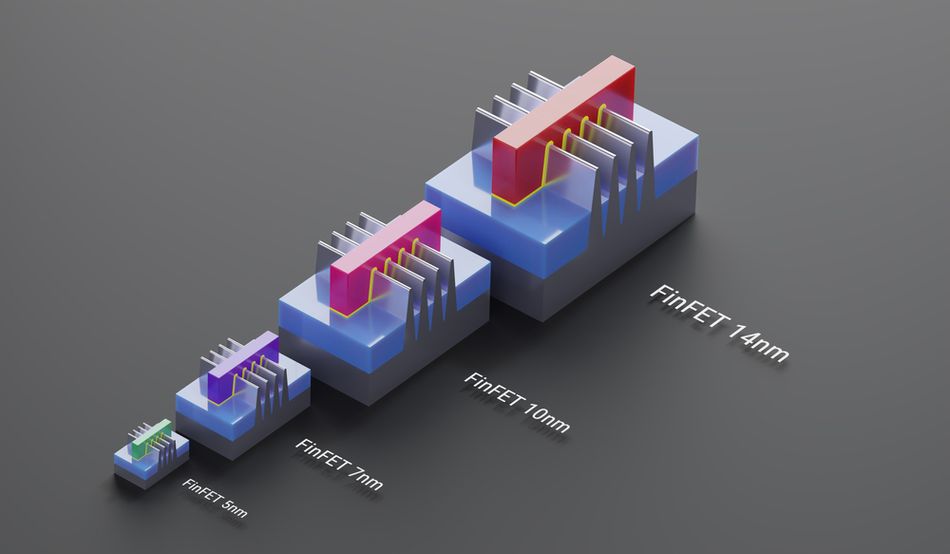
FinFETs, first adopted at 22 nm, now dominate microprocessor fabrication through 7 nm and beyond. Pushing further, Gate-All-Around (GAA) architectures offer 360° gate coverage around nanowire or nanosheet channels, delivering even greater control. Foundries like TSMC and Samsung are deploying GAAFETs at 3 nm and 2 nm nodes, enabling higher drive current, reduced leakage, and continued Moore’s Law scaling. These voltage-controlled devices provide exceptional switching performance and are key enablers of next-generation CPUs, AI accelerators, and mobile SoCs.
Superjunction and Advanced Power MOSFETs
In power supply applications, the trade-off between breakdown voltage and RDS(on) in silicon MOSFETs was a long-standing barrier. Superjunction MOSFETs overcome this using alternating p-type and n-type regions in the drift region to balance charge. This structure allows high doping (for low resistance) while still withstanding high voltages. Devices like CoolMOS series by Infineon have reduced RDS(on) by several factors over planar types.
For instance, a 600 V superjunction MOSFET today may achieve 10 mΩ on-resistance, enabling highly efficient DC-DC converters or motor controllers operating above 100 kHz. With reduced capacitance and lower gate charge, these switches exhibit fast transitions, though careful gate drive design is essential to manage dV/dt and ringing.
Trench and Shielded Gate Structures
In sub-200 V applications, trench gate MOSFETs dominate! By etching the gate terminal vertically into silicon, designers can pack more channel width per mm², drastically lowering RDS(on). Shielded gate trenches introduce a field plate to reduce Miller capacitance (Cgd), improving switching speeds by mitigating feedback coupling during fast edges.
These structures are widely used in power adapters, lighting inverters, and automotive ECUs. Their high cell density and low losses make them ideal for compact, high-efficiency systems.
Smart Power Integration
Smart Power ICs integrate MOSFETs with built-in gate drivers, protection circuits, and sensors. These single-package solutions simplify design and improve reliability. For instance, automotive high-side switches monitor VGS, temperature, and current, disabling the MOSFET under fault conditions. This is made possible by BCD processes, which combine bipolar, CMOS, and DMOS elements.
Today, FinFETs, JFETs in logic or superjunctions in power, represent decades of innovation. Through structural and architectural evolution, they continue to deliver unmatched performance in increasingly demanding applications.
Recommended Reading: Understanding JFET Technology: Applications and Misconceptions
Advanced Techniques Reveal Sophisticated Applications
Engineers have now developed advanced techniques that unlock powerful applications across power, analog, and mixed-signal domains. These approaches creatively exploit the intrinsic characteristics of MOSFET—such as gate capacitance, threshold voltage (Vth), and RDS(on)—turning design challenges into practical solutions.
Synchronous Rectification
In power supply circuits, replacing diodes with actively controlled MOSFETs dramatically reduces conduction losses. Known as synchronous rectification, this technique uses low RDS(on) MOSFETs to conduct current with significantly lower voltage drop compared to diodes. For instance, a diode may drop 0.7 V at 10 A (7 W loss), while a 5 mΩ MOSFET drops just 0.05 V (0.5 W). This method is now standard in DC-DC converters, laptop chargers, and CPU VRMs, boosting efficiency by up to 3%. However, precise gate control is critical—timing must avoid shoot-through, often handled by dedicated driver ICs.
Half-Bridge and Full-Bridge Applications
MOSFET half-bridges are at the heart of Class D amplifiers and motor drivers. These circuits switch MOSFETs at high frequencies (>300 kHz) to generate PWM waveforms. [4] In audio systems, this allows efficient power delivery with minimal heat. In motor control, H-bridges enable field-oriented control of brushless DC motors, used in EVs and drones. Driver ICs with dead-time control, VGS monitoring, and shoot-through protection are vital for reliable operation.
Charge Pumps and Voltage Doublers
MOSFETs serve as dynamic analog switches in charge pump circuits that generate internal high voltages—often >20 V from a 5 V rail—within flash memory or display drivers. These circuits rely on bootstrapping techniques to drive the gate terminal above the source, ensuring full enhancement. The performance depends on managing gate capacitance and threshold voltage to minimize loss.
Voltage-Controlled Resistors and Analog Multipliers
In analog design, a MOSFET in the linear region acts as a voltage-controlled resistor, useful in filters, attenuators, and modulators. Because of non-linearity, linearization techniques—such as dual-MOSFET structures with op-amp feedback—are used to create precision analog multipliers and tunable resistive elements.
Current Mirrors and Active Loads
MOSFETs form the basis of current mirrors and active loads in analog ICs. By using matched devices, engineers generate stable bias currents and achieve high gain in amplifier stages. Cascoded mirrors improve output resistance, enhancing current source behavior in op-amp design.
Cascode Configurations
The cascode configuration stacks MOSFETs to increase bandwidth and reduce the Miller effect. Often used in RF amplifiers, it isolates sensitive nodes from large voltage swings. In power circuits, combining a GaN FET with a low-voltage MOSFET simplifies gate driving, leveraging each technology’s strengths.
Transmission Gates
A transmission gate uses complementary n-channel and p-channel MOSFETs to pass analog signals bidirectionally. It’s essential in CMOS multiplexers, sample-and-hold circuits, and analog switches. These gates maintain flat on-resistance across voltage ranges, ensuring high signal fidelity.
In conclusion, these advanced techniques highlight the adaptability of a MOSFET. From nearly lossless switching to precision analog control, engineers continue to extract more from the same building block by applying smart, system-level design principles.
Quantitative Performance Metrics Guide Engineering Decisions
Selecting the right MOSFET for a given application involves more than checking voltage or current ratings.
Engineers depend on detailed quantitative metrics to evaluate how a device will perform in real circuits—balancing efficiency, reliability, and cost.
Key Metrics and Trade-Offs
The most referenced figure is RDS(on)—the on-state resistance between drain and source. Low RDS(on) reduces I²R conduction losses and is essential in power supply and converters handling high currents. However, lower resistance often means a larger die, which increases gate charge (Qg) and capacitance, making the MOSFET slower to switch.
To evaluate overall efficiency, engineers often refer to Figures of Merit (FOMs). One common FOM is:
RDS(on) × Qg
A lower product indicates a well-balanced device for high-frequency switching: low resistance with minimal drive energy. For synchronous rectifiers, another FOM is:
RDS(on) × Qrr (reverse recovery charge)
This helps assess both conduction and body diode switching loss—critical in applications with hard-switching transitions or high-frequency operation.
Drive and Thermal Considerations
Every switching event requires energy to charge and discharge the gate terminal. For example, a device with Qg = 50 nC at 1 MHz switching frequency needs to move 50 µC per second—averaging 50 mA of gate drive current, plus higher peak currents. Engineers must ensure the gate driver can source/sink that current efficiently without introducing delays.
Thermal management is another key area! MOSFETs dissipate power from both conduction and switching losses, and the resulting heat must be managed. Datasheets provide:
Thermal Resistance
Transient Thermal Impedance
Maximum Junction Temperature
Engineers calculate power dissipation and check against these to design proper cooling solutions like heatsinks or thermal vias.
Analog Metrics: gm and ro
In analog applications, two essential parameters are transconductance (gm) and output conductance (ro).
gm (in mA/V or S) measures how strongly the drain current reacts to changes in VGS. Higher gm translates to better gain in amplifier stages.
ro, the inverse of output conductance, reflects the device's ability to behave like an ideal current source. High ro (low channel length modulation) improves linearity and gain.
Designers often refer to gm/ID plots to select the optimal operating point for low noise, efficiency, or dynamic range.
Temperature Coefficients
MOSFET characteristics shift with temperature! RDS(on) usually increases with temperature (positive coefficient), which can help with current sharing when paralleling devices. Vth (threshold voltage) decreases slightly (negative coefficient), affecting turn-on behavior and leakage current in hot environments. Engineers ensure that, even under worst-case high temperatures, MOSFETs remain properly biased to avoid unintended conduction.
Safe Operating Area (SOA)
SOA charts and avalanche energy ratings (e.g., can it withstand a 50 A, 1 ms pulse or a 100 µJ avalanche event) help verify if a MOSFET can handle transients without failure. Adhering to these ensures long-term device reliability.
Selecting the right MOSFET involves mastering a matrix of parameters—RDS(on), Qg, Vth, capacitance, and thermal limits. By comparing these values to the switching frequency, drive strength, and power dissipation of different applications, engineers can design optimized, reliable systems.
Recommended Reading: JFET vs MOSFET: A Comprehensive Engineering Analysis and Selection Guide
Future Directions Integrate GaN and SiC
Looking forward, the future of transistor technology – especially in power electronics – is being shaped by wide-bandgap (WBG) semiconductors, chiefly Gallium Nitride (GaN) and Silicon Carbide (SiC).
These materials are enabling MOSFET-like devices that can operate at voltages, frequencies, and temperatures that silicon power MOSFETs can’t reach, thereby complementing or even replacing silicon in many applications.
Silicon Carbide (SiC) MOSFETs
SiC is a WBG material with a bandgap of ~3.3 eV—nearly three times that of silicon. Its high breakdown electric field allows the fabrication of MOSFETs that operate efficiently at 900 V, 1200 V, and even 1700 V. This makes them ideal for applications like EV traction inverters, solar power systems, and industrial motor drives.
Unlike traditional IGBTs, SiC MOSFETs switch faster and eliminate tail current losses, enabling higher efficiency and smaller magnetics. For example, in an 800 V DC bus EV inverter, SiC reduces current levels and conduction losses, improving both range and system reliability. Operating temperatures can reach 175°C or more, thanks to SiC’s thermal stability—perfect for harsh automotive and aerospace environments.
However, SiC poses challenges! It requires higher VGS drive voltages (typically +18 to +20 V), and its parasitic body diode has slower recovery than silicon, demanding more careful circuit design. Cost has also been a barrier—SiC wafers are smaller and more expensive—but volume production for EVs is driving prices down rapidly. SiC is now viewed as the high-power extension of the silicon MOSFET, especially between 600 V and 1700 V. [5]
Gallium Nitride (GaN) Transistors
GaN is another WBG material (bandgap ~3.4 eV), offering a different performance profile. Commercial GaN transistors—often built as enhancement-mode devices or cascode structures—are capable of extremely fast switching, due to their low capacitances and gate charge (Qg).
Where GaN excels is speed! Devices can switch at 1–2 MHz, even up to 150 MHz in some integrated designs. This enables ultra-compact power supplies, chargers, and RF systems with dramatically reduced inductor and capacitor sizes. The lack of a traditional body diode in GaN eliminates reverse recovery losses (Qrr), simplifying half-bridge converter designs and improving high-frequency performance.
Currently, GaN is most common in 100 V to 650 V applications: USB-C laptop chargers, server PSUs, telecom infrastructure, and RF amplifiers. Its RDS(on) is competitive with silicon, but the switching losses are much lower due to its extremely small Qg. Some GaN ICs now integrate the gate driver and control logic directly on-die—reducing parasitics and making power-stage-on-chip designs viable.
Complementary Use: Si vs. SiC vs. GaN
The landscape can be visualized like this:
Silicon: Ideal for <600 V, cost-effective consumer devices
GaN: Best for <650 V, high-speed, high-frequency applications
SiC: Suited for >650 V, high-power and high-temperature systems
There is overlap near the 600 V mark, where application requirements guide selection. For example, a 650 V GaN transistor might be ideal in a high-frequency server PSU, while a 1200 V SiC MOSFET would better serve an EV traction inverter or solar farm.
Integration and Hybrid Solutions
Emerging solutions integrate GaN FETs, drivers, and controllers into compact, monolithic ICs—reducing design complexity and improving EMI performance. Some devices offer dual GaN transistors in half-bridge configurations, complete with shoot-through protection, thermal monitoring, and digital control interfaces.
Meanwhile, hybrid modules are appearing where SiC or GaN is co-packaged with silicon MOSFETs or controllers. For example, a GaN FET may handle high-speed switching, while a low-voltage silicon MOSFET provides startup regulation or current limiting.
Engineering Implications
For engineers, working with GaN and SiC introduces new paradigms. dV/dt rates can exceed 100 kV/μs, demanding PCB layouts with minimal inductance and controlled impedance—akin to RF design. Heat sinks, EMI shielding, and magnetic components must be re-evaluated, especially as switching frequencies climb beyond 1 MHz.
Furthermore, gate drive requirements differ: GaN typically needs precise 5–6 V VGS with tight control, while SiC often requires +20 V / -5 V swing to avoid false turn-on or shoot-through. Designers must use dedicated gate drivers tailored to each device type.
GaN and SiC are not replacements for silicon—they are enhancements to the MOSFET toolkit. They expand the voltage, temperature, and frequency range of what’s possible in power electronics.
In the next decade, engineers who understand how MOSFETs work will find that their knowledge directly translates to designing with WBG devices—only now, the stakes (and capabilities) are much higher. From ultra-compact chargers to high-voltage EV inverters, GaN and SiC are leading the charge into a faster, more efficient future of semiconductor control.
Recommended Reading: Next-generation MOSFET Technology Meets Demand for Strong Thermal Performance in Automotive Applications
Conclusion
In 2025, the answer to how do MOSFETs work spans far beyond basic transistor theory. It encompasses a broad spectrum—from mastering gate voltage control and threshold modulation to implementing high-efficiency power converters and scaling digital logic to the nanometer frontier. This guide explored MOSFET behavior across diverse applications, emphasizing how foundational knowledge enables innovation in both analog and digital realms. Looking ahead, tighter integration, smarter driver circuits, and the rise of GaN and SiC technologies will further extend the MOSFET’s reach into higher voltage, frequency, and temperature domains. Whether enabling compact EV inverters or efficient server power supplies, MOSFETs will remain central. By understanding how MOSFETs work—both in principle and in practice—engineers are poised to shape the next generation of efficient, reliable, and scalable electronics.
FAQ (Frequently Asked Questions)
Q1: Why use a MOSFET instead of a BJT (bipolar transistor)?
A: MOSFETs are voltage-controlled with high input impedance, draw little gate current, switch faster, and have lower conduction losses than BJTs—making them more efficient and easier to drive in power and logic applications.
Q2: Why do MOSFETs often need a dedicated gate driver?
A: The gate behaves like a capacitor and requires high peak currents for fast switching. Gate drivers provide strong, controlled VGS, reduce transition time, and protect against under-drive and shoot-through faults.
Q3: What is the threshold voltage of a MOSFET, and why isn’t it the same as the turn-on voltage?
A: Threshold voltage is when conduction just begins, but full enhancement needs higher VGS. Designers must apply sufficient overdrive voltage for efficient switching, depending on the application and desired drain current.
Q4: How do I choose the right MOSFET for my application?
A: Match voltage, current, RDS(on), gate charge, package, and thermal needs. Balance switching speed vs. conduction loss, and ensure proper VGS levels and FOM values for efficiency and thermal reliability.
Q5: Do modern CPUs really contain MOSFETs? How many?
A: Yes—billions. CPUs use CMOS logic built entirely from MOSFETs. For example, Apple’s M3 Ultra has around 184 billion transistors, all of which are MOSFETs enabling logic, memory, and control functions.
Q6: What’s the difference between silicon MOSFETs and newer GaN or SiC transistors?
A: GaN and SiC switch faster, handle higher voltages or temperatures, and offer better efficiency. They require specialized drivers and cost more, but outperform silicon in power, speed, and high-frequency applications.
Q7: What is the MOSFET body diode, and how does it affect electronic circuits?
A: The body diode conducts during dead time or the reverse flow of current. It has slow recovery and higher losses, so designers often replace or avoid it in fast-switching applications using synchronous control.
References
[1] Wevolver. Difference Between P-Type and N-Type Semiconductors [Cited 2025 July 05] Available at: Link
[2] Apple. Apple Reveals M3 Ultra, taking Apple Silicon to a New Extreme [Cited 2025 July 05] Available at: Link
[3] UCSD. HSPICE User Guide: Simulation and Analysis [Cited 2025 July 05] Available at: Link
[4] TJHXPCB. H-Bridge Motor Controller Guide | Components, Applications [Cited 2025 July 05] Available at: Link
[5] MDPI. The Road to a Robust and Affordable SiC Power MOSFET Technology [Cited 2025 July 05] Available at: Link
in this article
1. Introduction2. Theoretical Foundations Reveal How MOSFETs Work3. Design Techniques Leverage Threshold Modulation4. Common Applications Span from Computing to Power Control5. Integration with Gate Drivers Enables Fast Switching6. Modern Software Tools Revolutionize MOSFET Implementation7. Best Practices Address Common Implementation Pitfalls8. Recent Developments Push Boundaries of Semiconductor Control9. Advanced Techniques Reveal Sophisticated Applications10. Quantitative Performance Metrics Guide Engineering Decisions11. Future Directions Integrate GaN and SiC12. Conclusion13. FAQ (Frequently Asked Questions)14. References