What is GND in a Circuit: The Complete Guide for Digital Design and Hardware Engineers
Master circuit grounding fundamentals, from voltage references to EMI control, with practical implementation strategies for modern electronics design.

07 Jul, 2025. 15 minutes read
Key Takeaways
GND serves three critical functions: voltage reference point (0V baseline), current return path for circuit completion, and EMI/safety control mechanism
Ground impedance matters more than resistance at frequencies above 1 MHz, making proper high-frequency design essential for signal integrity
Single continuous ground planes outperform split ground approaches in modern mixed-signal designs, contrary to outdated practices
Ground loops cause major interference but can be prevented through single-point grounding, differential signaling, or galvanic isolation
Proper measurement requires specialized equipment: standard DMMs cannot accurately measure the ≤2.5 mΩ resistance required by automotive and aerospace standards
Introduction
The most perfectly designed electrical circuits can be plagued by mysterious noise, intermittent failures, and EMI test failures. The culprit? Poor grounding—the silent killer of electronic designs. While every circuit diagram shows ground symbols liberally scattered throughout, few engineers truly understand the complex physics and practical implications of GND in modern circuits.
Ground, or GND, is more than just a simple connection point in electronic circuits. For digital design engineers and hardware engineers working with today's high-speed systems, understanding ground is the difference between a product that ships and one that fails compliance testing. As switching frequencies push beyond gigahertz ranges and mixed-signal designs become the norm, the traditional "ground is ground" mentality no longer suffices.
This comprehensive guide discusses circuit grounding to provide practical, implementable solutions for real-world design challenges. This article discusses the fundamental physics, advanced measurement techniques, examining how ground functions differently at DC versus high frequencies, why ground loops form, how to eliminate them, and which grounding strategies work best for specific applications.
Understanding the Fundamentals of Ground in Electronic Circuits
Ground represents the foundation of every electronic circuit, yet its true nature often eludes even experienced engineers. At its core, ground serves as the 0V reference point against which all other voltages in a circuit are measured. However, this simple definition masks the complex reality of how ground functions in modern electronics.
Ground and Frequency Dependent Behavior
Ground planes exhibit finite resistance and impedance, creating voltage differences across the ground system. At DC and low frequencies, current follows the path of least resistance through the ground plane. But as frequencies increase above 1 MHz, the current now follows the path of least impedance, typically flowing directly underneath signal traces to minimize loop area.
This frequency-dependent behavior explains why a design that works perfectly on the bench might fail spectacularly during EMC testing. For instance, a digital signal with 1-nanosecond rise time: its return current contains frequency components up to 350 MHz, turning every inch of ground trace into a significant inductor. The resulting ground bounce can corrupt data, trigger false logic states, and radiate electromagnetic interference that violates regulatory limits.
Circuit Ground Symbols
Depending on the type of ground, there are various symbols to make it easier for designers and engineers to implement grounding in physical systems. Here is a quick look at the various symbols. Standard ground symbols often contribute to confusion rather than clarity.
Signal ground symbol: Depicted as an empty triangle pointing downwards, or sometimes as three parallel horizontal lines of decreasing length, with the shortest at the bottom.
Chassis ground symbol: Often represented by three parallel diagonal lines pointing downwards.
Earth ground symbol: Illustrated as three parallel horizontal lines of decreasing length, with the longest at the top and the shortest at the bottom.
These distinct symbols visually differentiate the various types of grounds, ensuring clarity and precision in electrical schematics.
Suggested Reading: Circuit Symbols: A Comprehensive Guide for Electronics Engineers
Types of Ground and Their Applications
Modern electronic systems employ multiple ground types, each serving distinct purposes that engineers must understand to create robust designs. The proliferation of mixed-signal systems makes proper ground type selection and implementation more critical than ever.
Signal Ground
Signal ground divides into two crucial subcategories, i.e., Analog ground and Digital ground. They manage return paths for different types of signals to maintain integrity.
Signal Ground Type | Description | Applications |
Analog Ground (AGND) | Provides the ultra-clean reference required for sensitive measurements and low-noise amplifiers. |
|
Digital Ground (DGND) | Handles the aggressive return currents from fast-switching logic, tolerating higher noise levels. |
|
Virtual Ground
Virtual ground represents a clever circuit technique where a point in a circuit is held at a reference potential (often 0V) by active components, without being physically connected to a true ground. The applications of virtual ground include:
Creating a mid-supply reference in single-supply circuits to enable bipolar signal processing
Active filters
Voltage followers (as a reference point for feedback)
Precision current-to-voltage converters
Single-supply systems often create virtual grounds at half the supply voltage, enabling bipolar signal processing without negative power rails. However, virtual grounds cannot sink unlimited current like true grounds—a limitation that trips up many designers transitioning from dual to single-supply designs.
Earth Ground
Earth ground primarily functions as a safety mechanism, offering a low-impedance path for fault currents to protect users from electric shock and to dissipate static charges or lightning strikes. Earth ground is commonly found in:
Safety grounding for most powered electrical equipment (e.g., household appliances, industrial machinery)
Lightning protection systems for buildings and outdoor structures
Static discharge paths in industrial environments (e.g., fuel handling, electronics manufacturing)
Grounding of power distribution grids
Ensuring regulatory compliance (e.g., UL, CE standards) for electrical products
Chassis Ground
Chassis ground refers to connecting a circuit's common return path to the metallic frame, enclosure, or body of a device or vehicle, serving as a common reference and protective barrier. Its applications include:
Common return path in automotive electrical systems (e.g., car body, motorcycle frame)
EMI/RFI shielding for electronic enclosures and equipment
Safety grounding of metal casings in electronic devices
Providing a common electrical reference point within a device or system
Industrial control panels and equipment enclosures
 Fig 2: Copper ground strap connected to a car’s body
Floating Ground
A floating ground is an isolated electrical reference point that is not directly connected to earth ground or any other common ground. It is used to provide galvanic isolation, preventing current flow between different potential levels. Its applications include:
Medical devices (e.g., patient monitoring equipment) are used to prevent dangerous leakage currents.
Industrial instrumentation to break ground loops between equipment at different potentials.
Battery-powered devices with no direct connection to a utility ground.
Isolated power supplies and data communication interfaces (e.g., optocouplers).
Suggested Reading: Linear vs Switching Power Supply: Understanding the Differences
Ground Planes in Modern PCB Design
The shift from through-hole to surface-mount technology fundamentally changed PCB grounding strategies. Modern PCB design practices emphasize continuous, unbroken ground planes that provide low-impedance return paths for all signals. This approach replaces the outdated "ground traces" mentality that plagued early PCB designs.
Four-layer PCBs
Four-layer PCB stackups have become the minimum standard for serious digital designs, dedicating entire layers to ground planes. The typical stackup places signals on layers 1 and 4, with ground on layer 2 and power on layer 3.
This arrangement provides excellent signal integrity through close coupling between signals and their return paths, while the power-ground plane pair creates distributed decoupling capacitance that filters high-frequency noise.
Recommended Reading: PCB Stackup Optimization: Engineering Robust Electronics
Via Stitching
Via stitching helps in maintaining ground plane integrity across layers. Ground vias should be placed every 1/10 wavelength at the highest frequency of interest—for a 1 GHz signal, this means vias every 30mm around the PCB perimeter and at ground plane transitions.
Modern PCB design tools can automatically place stitching vias; however, engineers must verify adequate coverage, especially near high-speed signals that cross layer boundaries.
Thermal Relief
Thermal relief patterns are necessary for manufacturing. However, they can compromise ground integrity if not properly implemented. High-current connections require multiple vias or direct plane connections to minimize resistance.
For precision analog circuits, some designers eliminate thermal reliefs on critical ground connections, accepting increased assembly difficulty in exchange for superior performance.
Suggested Reading: Aluminum PCB Design: Advanced Thermal Management Solutions for High-Power Electronics
Implementing Effective Grounding Architectures
The eternal debate between single-point and multipoint grounding strategies has largely been resolved by frequency domain analysis.
Single-point grounding excels below 1 MHz, where ground impedance remains predominantly resistive. Audio equipment and precision instrumentation often employ star grounding to eliminate ground loops and minimize crosstalk between circuits.
Multipoint grounding is essential for frequencies above 10MHz. The inductance of long ground connections creates unacceptable impedance at high frequencies, forcing multiple short connections to the ground plane. Modern digital circuits, including low-speed microcontrollers, operate far above this threshold, making multipoint grounding through a continuous plane the only viable option.
Hybrid Grounding
Mixed-signal designs demand a nuanced approach that seemingly contradicts conventional wisdom. Single continuous ground plane with intelligent component placement is a modern approach to handling grounding for mixed signals.
Typically, analog and digital sections occupy different PCB regions, with careful attention to where return currents naturally flow. This approach, validated by simulation and measurement, provides superior performance compared to split planes in most applications.
Suggested Reading: PCB Layers: Everything You Need to Know
The hybrid grounding strategy emerges as the optimal solution for complex systems.
Low-frequency and DC connections use single-point grounding to prevent ground loops
High-frequency signals employ multipoint connections to the ground plane.
Ferrite beads or small inductors separate these grounding domains, appearing as open circuits at high frequencies while maintaining DC continuity.
Identifying and solving ground loop problems
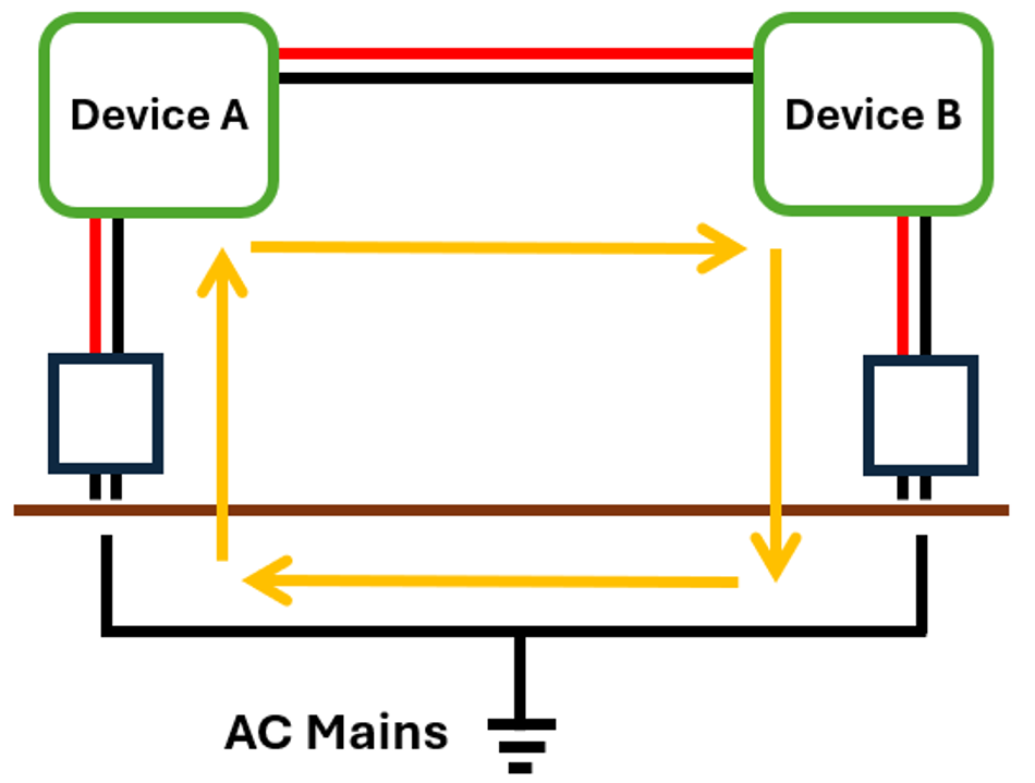
Ground loops are sneaky issues in electronics that cause interference. They happen when there are multiple ground connections between different pieces of equipment, letting unwanted currents flow through the ground paths. These currents create voltage differences, which then corrupt signals, add noise, and can even harm sensitive components.
How Ground Loops are Formed
Consider a scenario where two devices are connected by both signal cables and AC mains grounds. Mains grounds often have slightly different potentials at various locations. This potential difference drives current through the signal ground, creating the loop.
Impact of Ground Loops
Audio Systems: Often heard as a 60 Hz (or 50 Hz) hum.
Data Systems: Leads to bit errors and communication failures.
Industrial Settings: Large motors or welding equipment can cause significant ground potential differences, sometimes several volts.
Breaking Ground Loops
Solving ground loops means stopping these unwanted current paths.
Technique | Description | Applications/Examples |
Differential Signaling | Sends signals on two lines, making them immune to ground potential differences. | RS-485, CAN bus, LVDS, balanced audio cables |
Isolation | Breaks the direct electrical (galvanic) connection. | Isolation transformers (audio, power), optocouplers (data) |
Measuring and Mitigating Ground Bounce
Ground bounce is a major challenge in high-speed digital design. It occurs during transistor switching, when rapid current changes across ground impedance create voltage fluctuations. These transient voltages can falsely trigger logic, corrupt data, and cause timing issues.
Measuring Ground Bounce
Accurate measurement of ground bounce requires specialized techniques:
"Quiet Low" Method: Logic outputs are programmed to stay low as sense lines, revealing ground disturbances without probe interference.
High-Frequency Probing:
For measurements above 100 MHz, differential probes or dedicated power rail probes are essential.
Instruments like the Teledyne LeCroy RP4030 offer the necessary millivolt resolution and high bandwidth for sub-nanosecond disturbances.
Mitigating Ground Bounce
Effective mitigation goes beyond simple capacitor placement:
Strategic Bypassing:
Place bypass capacitors within 3mm of IC power pins to minimize inductance.
Move beyond the "0.1 µF everywhere" rule for modern speeds.
Use multiple capacitor values (e.g., 10 µF, 1 µF, 0.1 µF, 1000 pF) to cover the full frequency spectrum, with smaller values closest to the IC.
Power & Ground Plane Pairs:
These adjacent, closely spaced layers (e.g., 0.1mm separation) provide distributed capacitance.
They offer high-frequency bypassing directly where needed (approx. 100 pF per square centimeter).
Via-in-pad technology further reduces connection inductance, improving performance and reducing EMI despite higher manufacturing costs.
Suggested Reading: Via in Pad PCB Design
EMI Control through Proper Grounding
Electromagnetic interference (EMI) is a significant problem in electronics, often stemming from improper grounding. Every ground connection both provides signal return paths and controls electromagnetic fields. Understanding this dual role transforms EMI mitigation from a mystery into an engineering discipline.
How Ground Systems Control EMI
Ground systems manage EMI through two main mechanisms:
Low-Impedance Paths: Minimize voltage differences that drive unwanted radiation.
Shielding: Ground planes reflect and absorb electromagnetic fields.
Crucial Point: A seemingly minor ground plane split at DC can become a significant slot antenna at gigahertz frequencies, compromising effectiveness.
Common-Mode Currents
Common-mode currents are the primary radiation source in most systems. These currents flow in the same direction on signal and ground conductors, effectively turning cables into antennas.
Mitigation: Proper grounding minimizes common-mode generation by ensuring return currents flow immediately adjacent to their corresponding signals.
Loop Area: If signal and return paths are forced to separate, the enclosed loop area directly determines radiation intensity; every square millimeter is critical for meeting stringent EMC requirements.
Modern EMC Standards
Modern EMC standards have evolved for high-speed digital systems:
Automotive (e.g., ISO 11452): Mandates ground bonding resistance below 2.5 milliohms, measured with specialized four-wire instrumentation.
Military/Aerospace (e.g., MIL-STD-461G): Imposes similar strict requirements, recognizing the direct impact of ground integrity on both emissions and susceptibility.
Suggested Reading: EMI Shielding: Protecting Electronic Devices in a Noisy World
Troubleshooting Ground Issues
Grounding issues are often overlooked, but they are often the core reason behind circuit failures. Hence, a systematic troubleshooting approach saves time and avoids aimless "shotgun debugging."
Diagnosing Ground Problems
Start by mapping current flow paths, not just connections.
Measurement Tools & Techniques:
Oscilloscope: Measure voltage differences between "connected" ground points; even millivolts indicate high-frequency issues.
Four-Wire Resistance: Reveals DC grounding issues invisible to standard multimeters.
Network Analyzer: Plots ground impedance vs. frequency, exposing resonances and poor bypassing.

Common Symptoms & Causes
Recognizing patterns accelerates diagnosis:
Random resets/lockups: Often, ground bounce affects digital logic.
Unexpected analog offsets: Suggests ground current through sensitive areas.
EMI test failures (specific frequencies): Indicates ground plane resonances or inadequate stitching.
Data corruption (worsens with cable length): Implies ground loops between equipment.
Near-Field Probing
Near-field probing offers vital insight into ground current distribution.
Method: Use H-field probes (commercial or DIY) to detect magnetic fields from current flow.
Benefit: Visualize ground current paths, identify hot spots, and uncover unexpected current paths directly on the PCB, preventing costly redesigns.
Suggested Reading: Hipot Test: Ensuring Electrical Safety and Reliability
Future Trends in Grounding Technology
The push for higher speeds and greater integration is drastically changing how we approach grounding. As digital interfaces exceed 100 Gbps and frequencies hit 10 GHz, even tiny ground path imperfections impact signal integrity.
Embedded Component Technology
Embedded component technology is set to transform high-frequency grounding. Integrating bypass capacitors directly into PCB substrates drastically reduces parasitic inductance. Early adoption in telecom shows significant improvements in power integrity and EMI.
Advanced Simulation and AI
Next-gen simulation tools now model ground systems with incredible accuracy. Full-wave electromagnetic solvers predict current distribution, identify resonances, and optimize designs before fabrication. Machine learning algorithms are also starting to suggest grounding strategies based on past successful designs, speeding up the learning curve for engineers.
Automotive Electrification and Autonomy
The shift to electric vehicles (EVs) brings unique grounding challenges. High-voltage battery systems need sophisticated grounding for safety and to minimize EMI with sensitive electronics. Autonomous vehicles add further complexity with numerous high-speed sensors and processors requiring pristine ground environments.
Suggested Reading: Innovations in Electric and Autonomous Vehicles
Conclusion
Understanding ground in a circuit goes far beyond basic definitions; it's a complex, frequency-dependent system fundamental to performance, safety, and electromagnetic compatibility. The shift from simple DC concepts to sophisticated high-frequency ground management highlights electronics engineering's evolving demands.
Mastering grounding means discarding outdated ideas – ground isn't a perfect conductor, splits rarely help, and every connection has critical impedance at modern frequencies. By embracing physics-based understanding and measurement, engineers can build robust designs, ensuring better yields, easier compliance, and enhanced reliability. While future challenges will intensify with climbing frequencies and integration, the core principles remain: current must return, impedance varies with frequency, and proper grounding requires deliberate design, not assumption.
Frequently Asked Questions
What's the difference between the ground and negative terminal in a circuit?
Ground serves as the 0V reference point for all voltage measurements in a circuit, while the negative terminal simply indicates a power supply connection with potential lower than the positive terminal. In many circuits, the negative terminal connects to ground, making them functionally identical. However, in floating systems like batteries or isolated power supplies, the negative terminal has no direct connection to ground. Some circuits even use positive ground systems where the positive terminal connects to ground reference. The key distinction: ground defines the measurement reference for the entire system, while negative terminal only describes one power connection polarity.
Can I use a single ground plane for both analog and digital circuits?
Yes, modern best practice recommends using a single, continuous ground plane for mixed-signal designs rather than splitting grounds. The key to success lies in intelligent component placement and routing. Position analog components in one board region and digital components in another, allowing return currents to naturally remain separated. Route sensitive analog signals away from digital switching areas, and use proper power supply filtering between domains. This approach avoids the severe problems created by split ground planes, including forced return current paths through bottlenecks and increased electromagnetic emissions.
How do I measure ground resistance accurately for EMC compliance?
Standard digital multimeters cannot measure the milliohm-level resistances required for EMC compliance. You need a four-wire (Kelvin) measurement setup using a specialized milliohm meter or micro-ohmmeter. These instruments apply a known current through two leads while measuring voltage drop through separate sense leads, eliminating lead resistance from the measurement. For automotive and aerospace standards requiring ≤2.5 milliohm ground bonds, ensure your instrument can resolve to 0.1 milliohm or better. Always clean connection points thoroughly and apply appropriate contact pressure for repeatable results.
Why does my circuit work on the bench but fail EMC testing?
Bench setups often use short wires and compact layouts that mask grounding deficiencies. During EMC testing, longer cables and standardized test configurations expose ground impedance problems invisible at low frequencies. Common culprits include inadequate ground plane stitching, poor cable shield termination, and ground loops between equipment. The high-frequency content of digital signals—extending to hundreds of megahertz even for "slow" circuits—turns minor ground defects into efficient antennas. Solution: design and validate grounding systems at the frequencies where they'll be tested, not just where they operate.
When should I use star grounding versus multipoint grounding?
Star (single-point) grounding works best for frequencies below 1 MHz, where ground impedance remains primarily resistive. Audio equipment, precision analog instruments, and low-frequency power systems benefit from star grounding's ability to prevent ground loops and minimize crosstalk. Above 10 MHz, multipoint grounding becomes essential as ground inductance dominates impedance. Digital circuits, RF systems, and high-speed signals require multiple short connections to a continuous ground plane. Many systems use hybrid approaches: star grounding for DC and low-frequency paths combined with multipoint high-frequency grounding through bypass capacitors or ferrite beads.
How many ground vias do I need when changing layers?
The number of ground vias depends on signal frequency and current levels. For high-speed signals, place ground vias within 1/20 wavelength of the signal via—at 1 GHz, this means within 15mm. Use multiple vias to reduce inductance: each via exhibits approximately 1.5 nH inductance, so parallel vias reduce total inductance proportionally. For power connections carrying over 1A, use one via per amp minimum, with more for high-frequency switching currents. Around board perimeters and between ground plane sections, space stitching vias at 1/10 wavelength intervals. Modern autorouters can place vias automatically, but always verify adequate coverage manually.
References
- "Floating ground - Wikipedia." [Online]. Available: https://en.wikipedia.org/wiki/Floating_ground
- "Chassis, Earth and Signal Grounding: Terminology and Symbols - NI." [Online]. Available: https://www.ni.com/en/support/documentation/supplemental/18/chassis--earth-and-signal-grounding--terminology-and-symbols.html
- "An Introduction to Ground," All About Circuits. [Online]. Available: https://www.allaboutcircuits.com/technical-articles/an-introduction-to-ground/
- "PCB Ground Plane Best Practices in Your Multilayer Stackup," Altium Resources. [Online]. Available: https://resources.altium.com/p/pcb-ground-plane-best-practices-your-multilayer-stackup
- "What is Ground Bounce?" Cadence. [Online]. Available: https://resources.pcb.cadence.com/blog/what-is-ground-bounce
- "What is a ground loop?" CircuitBread. [Online]. Available: https://www.circuitbread.com/ee-faq/what-is-a-ground-loop
- "Basics of Ground Loops | What is Ground Loop ?" Instrumentation Tools. [Online]. Available: https://instrumentationtools.com/basics-ground-loops/
- "Designing Electronic Systems for EMC: Grounding for the Control of EMI," Interference Technology. [Online]. Available: https://interferencetechnology.com/designing-electronic-systems-for-emc-grounding-for-the-control-of-emi-3/
in this article
1. Key Takeaways2. Introduction3. Understanding the Fundamentals of Ground in Electronic Circuits4. Types of Ground and Their Applications5. Fig 2: Copper ground strap connected to a car’s body6. Ground Planes in Modern PCB Design7. Implementing Effective Grounding Architectures8. Identifying and solving ground loop problems9. Measuring and Mitigating Ground Bounce10. EMI Control through Proper Grounding11. Troubleshooting Ground Issues12. Future Trends in Grounding Technology13. Conclusion14. Frequently Asked Questions15. References