Featured
Two new kinds of on-skin electronics allow users to build and customize them directly on the body – with potential applications in biometric sensing, medical monitoring, interactive prosthetic makeup and more.

Two new kinds of on-skin electronics allow users to build and customize them directly on the body – with potential applications in biometric sensing, medical monitoring, interactive prosthetic makeup and more.
PCB Trace Width Calculator
Glossary of Semiconductors Terms
Two new kinds of on-skin electronics allow users to build and customize them directly on the body – with potential applications in biometric sensing, medical monitoring, interactive prosthetic makeup and more.
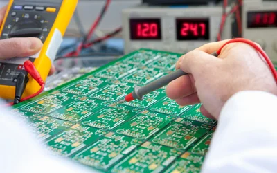
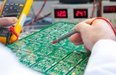
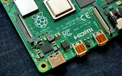
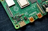
This article will guide you through the fundamentals of how to read a circuit board, decoding key elements, essential symbols and markings, exploring techniques for tracing circuits, and examining advanced analysis methods.
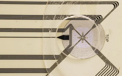
EPFL researchers have developed a novel neural recording device called the "e-Flower" that gently wraps organoids in soft petals.
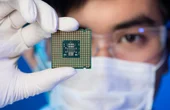
Semiconductors are the building blocks of modern electronics, powering everything from smartphones to satellites. This in-depth guide provides a comprehensive understanding of semiconductors' engineering principles and applications, delving into their fundamental concepts, materials, devices, manufacturing processes, and their impact on today's technology landscape.
13 minutes read.
20 minutes read.
16 minutes read.
20 minutes read.
20 minutes read.
13 minutes read.


Semiconductors
Nordic Semiconductor is a fabless semiconductor company specializing in wireless technology that powers the IoT.
181 Posts
A guide covering the full radio-frequency design workflow, starting from setting specifications and choosing topologies to matching, simulation, layout, and verification, to help antenna engineers.
This article presents a detailed technical exploration of SiC MOSFET devices, covering material physics, device structure, switching behavior, and practical design considerations for high-efficiency power electronics systems.
This article is a comprehensive technical guide to relay wiring diagrams, covering 4-pin and 5-pin configurations, working principles, safety practices, standards, and advanced relay applications in modern systems.
Explore how frequency shapes EMC behavior from RF emissions to ultra-low-frequency drift, with mitigation strategies for robust, compliant electronic system design.
How Essentra Components Supports Engineering from Concept to Production
Makera gives live demonstrations of the Z1 during the 2026 Hackaday Europe event. The Z1 is a compact CNC manufacturing platform.
A crystal oscillator is an electronic circuit that uses a quartz crystal to produce a precise and stable frequency reference. This article covers crystal operation, equivalent circuit models, resonance, load capacitance, oscillator topologies, stability, aging, and design practices.
June 25, 2026 at 08:00 PM Central European Summer Time
Two new kinds of on-skin electronics allow users to build and customize them directly on the body – with potential applications in biometric sensing, medical monitoring, interactive prosthetic makeup and more.

3 minutes read
This article will guide you through the fundamentals of how to read a circuit board, decoding key elements, essential symbols and markings, exploring techniques for tracing circuits, and examining advanced analysis methods.
EPFL researchers have developed a novel neural recording device called the "e-Flower" that gently wraps organoids in soft petals.
Learn how reliable and high-performance PCBAs are crucial for ensuring safe and efficient drone operation, ultimately contributing to the success of the offshore wind industry.

4 minutes read
In the final episode of Circuit Showdown, three contestants face their toughest challenge yet: integrating an IoT dashboard into their designs. With time running out, the judges are left with a tough decision. Who will rise to the occasion and win the championship?

2 minutes read
This article delves into the history and science behind the green color of circuit boards, shedding light on the reasons and advantages that have kept it at the forefront of electronics manufacturing.
Delve into the basics of absolute encoders, its applications, advancements in technologies, calibration techniques, and the advantages over encoder types.
MacroFab's FabIQ aims to disrupt this status quo by leveraging artificial intelligence and a vast database to provide instant, accurate pricing for printed circuit board (PCB) assemblies and panels.
2 minutes read
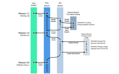
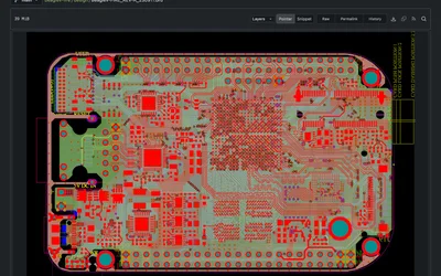
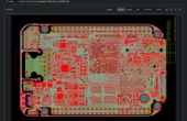
AllSpice is a Git-based collaboration platform that transforms hardware development by streamlining project workflows, enhancing design precision, and reducing time to market through established software engineering practices such as Agile and CI/CD.
High-frequency circuits-like those utilized in microcells and DAS-are more sensitive to PCB material selection, fabrication, and assembly.
8 minutes read
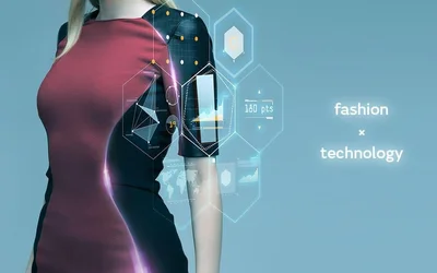
'Fashion tech' refers to the use of big data, AI, AR/VR, and IT in customer services; the development of products incorporating functional materials and wearable devices; and the application of electronics and digital technologies in manufacturing, processing, and distribution processes.

4 minutes read
Dr. Yuxuan Cosmi Lin and a team of researchers are studying the advantages of using semi-metals in different applications.

3 minutes read
Discover how flux and solder merge to form solder paste, a vital ingredient in the reliability of electronics.

5 minutes read
The fragmented nature of traditional hardware development tools calls for the adoption of a unified, technology-driven approach that integrates robust version control systems like Git alongside methodologies similar to agile and DevOps to streamline processes and enhance team collaboration.
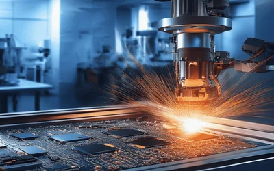
A team of academic and enterprise researchers has developed a synthesis process to produce a “rust-resistant” coating with additional properties ideal for creating faster, more durable electronics.

4 minutes read