Featured

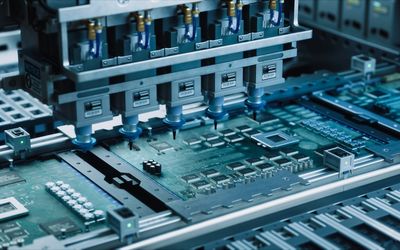
Printed electronics, characterized by their low cost and versatility through processes like inkjet or screen printing, are pivotal in advancing technologies such as wearable tech and the Internet of Things.

This guide is written for engineers and technical teams building connected devices who need clear, field-ready guidance without getting lost in standards documentation.
PCB Trace Width Calculator
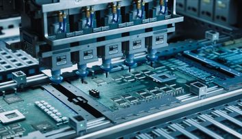
Printed electronics, characterized by their low cost and versatility through processes like inkjet or screen printing, are pivotal in advancing technologies such as wearable tech and the Internet of Things.
Selecting the right microcontroller (MCU) is crucial in embedded systems engineering, as it significantly influences the system's performance, power consumption, and overall success.
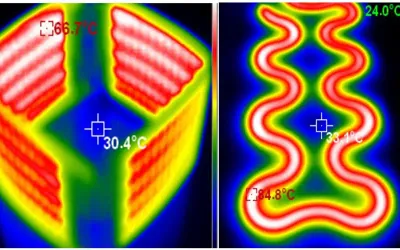
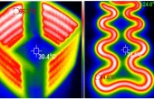
E2IP Technologies manufactures Flexible Heaters using Screen Printing Technology. This is one of the most important segments of printed and additive electronics with applications in cars, homes, and industrial settings.
Understanding the key differences between the two high-in-demand battery types. This article focuses on Energy density, lifespan, safety, and cost trade-offs for the technical selection of Li-Ion and LiFePO4 batteries.
16 minutes read.
20 minutes read.
15 minutes read.
20 minutes read.
13 minutes read.
28 minutes read.

Electronics
Mouser Electronics is a worldwide leading authorized distributor of semiconductors and electronic components.
219 Posts
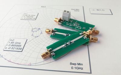
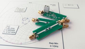
A guide covering the full radio-frequency design workflow, starting from setting specifications and choosing topologies to matching, simulation, layout, and verification, to help antenna engineers.
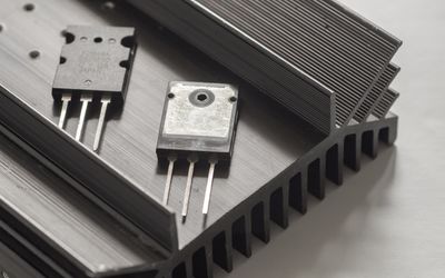
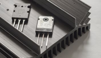
This article presents a detailed technical exploration of SiC MOSFET devices, covering material physics, device structure, switching behavior, and practical design considerations for high-efficiency power electronics systems.
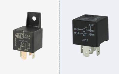
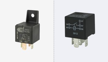
This article is a comprehensive technical guide to relay wiring diagrams, covering 4-pin and 5-pin configurations, working principles, safety practices, standards, and advanced relay applications in modern systems.
Explore how frequency shapes EMC behavior from RF emissions to ultra-low-frequency drift, with mitigation strategies for robust, compliant electronic system design.
Ultra-efficient chip design enables extremely strong cryptography algorithms to run on energy-constrained edge devices.
Researchers at ETH Zurich have now developed chip technology that enables verification of the authenticity of sensor data, including images or videos.
The integrated design achieves accurate micro gas chromatography and can help reduce the cost of monitoring chemical synthesis, natural gas pipelines or at-home air quality.
Hybrid bonding provides the adhesive free, copper to copper interconnects that are driving cutting edge 3D chip stacking. This article explains the theory, process, benefits, challenges, applications, and emerging trends of hybrid bonding for engineers.
Printed electronics, characterized by their low cost and versatility through processes like inkjet or screen printing, are pivotal in advancing technologies such as wearable tech and the Internet of Things.
Selecting the right microcontroller (MCU) is crucial in embedded systems engineering, as it significantly influences the system's performance, power consumption, and overall success.
E2IP Technologies manufactures Flexible Heaters using Screen Printing Technology. This is one of the most important segments of printed and additive electronics with applications in cars, homes, and industrial settings.

3 minutes read
Silver/silver chloride (Ag/AgCl) is a conductive ink typically used to print electrodes for biomedical applications.

3 minutes read
Explore and address needs in assistive technology, creating meaningful solutions for individuals with disabilities. Win great prizes!
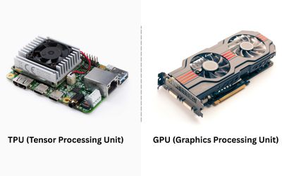
This article explores TPU vs GPU differences in architecture, performance, energy efficiency, cost, and practical implementation, helping engineers and designers choose the right accelerator for AI workloads today!
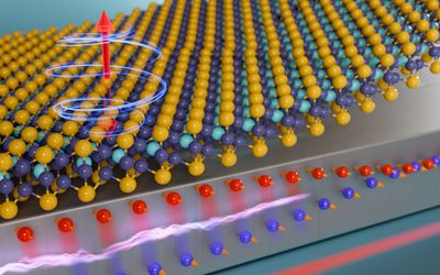
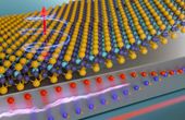
An MIT team precisely controlled an ultrathin magnet at room temperature, which could enable faster, more efficient processors and computer memories.
This article provides an in-depth exploration of the evolution, fundamental concepts, diverse types, operating principles, and practical applications of ASICs.
Startups in the hardware industry have an uphill battle to build a product that will break through in highly competitive markets. Only half survive beyond five years.

5 minutes read
LPWA is an abbreviation for Low-Power Wide-Area. It is also referred to as Low-Power Wide-Area Network (LPWAN). LPWA is wireless communication technology that features low power consumption and wide-area and long-distance communication.

15 minutes read
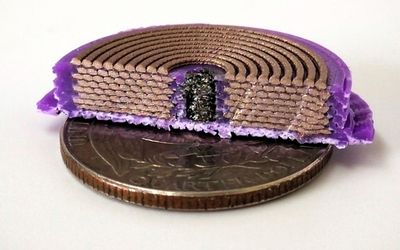
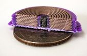
The printed solenoids could enable electronics that cost less and are easier to manufacture — on Earth or in space.
Edge AI and sensor fusion revolutionize tech by enabling instant, informed decisions through multi-sensor data analysis. Explore their application by building a Smart Running Jacket with Sony Spresense and SensiEDGE CommonSense via Edge Impulse platform.
Traditional HASL uses lead, raising environmental concerns. But how does ENIG compare?
5 minutes read
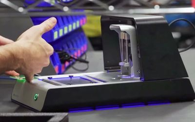
Voltera’s V-One benchtop printer is revolutionizing how electronics are developed with in-house, one-hour PCB prototyping.
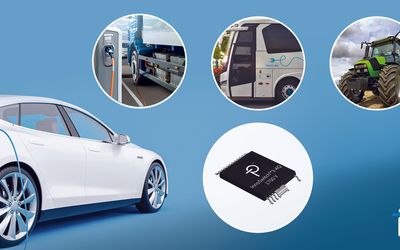
In the in-depth interview, PI Vice President of Marketing Doug Bailey explains GaN technology and the new possibilities it brings to the power conversion industry.

4 minutes read