Via Types: Essential Guide to Understanding and Utilizing in Electronic Design
Dive into the critical role of via types in modern electronics, exploring how they enhance connectivity and performance in circuit design. Learn about the latest advancements, practical applications, and challenges in using various via types.

30 May, 2024. 12 minutes read
Introduction
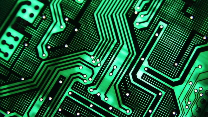
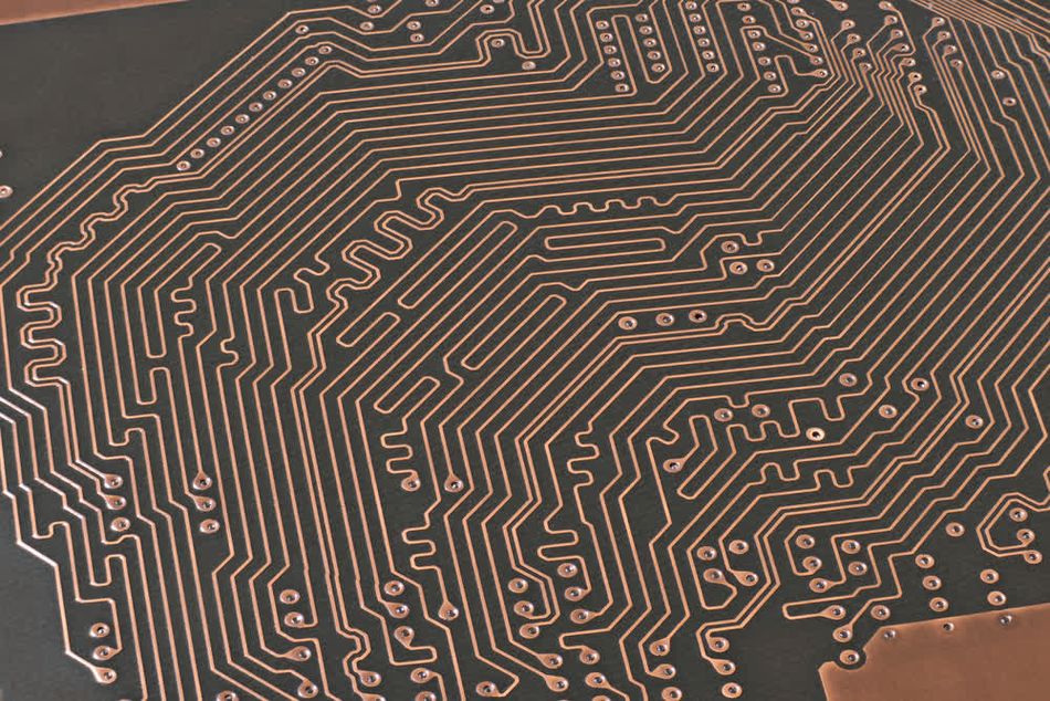
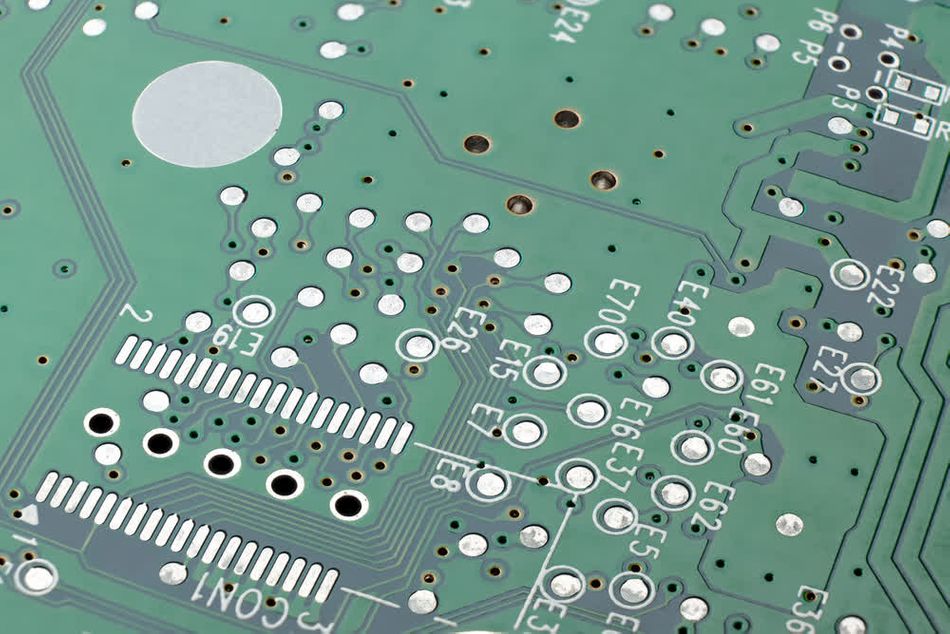
Vias are a critical part of PCB design as they allow different layers of a PCB to connect electrically. These are conductive paths that may not be physically visible on the surface of a PCB, but they facilitate the core operations, especially in multilayer PCBs to ensure proper functionality of circuit boards.
Based on the functionality, there can be several via types including:
Through-hole vias
Blind vias
Buried vias
Microvias (further divided into stacked and staggered vias)
In addition to ensuring electrical continuity, vias are also responsible for the structural integrity of a PCB. As they penetrate through various PCB layers, they provide structural reinforcement to the circuit board, to keep everything else in place.
Perhaps one of the major benefits of different via types is their contribution to miniaturization and enhancement of electronic devices. They facilitate innovations in design and functionality. As the complexity of electronic devices increases, so does the need for more sophisticated via technologies. This necessity drives the evolution of via types, which are pivotal not only for current engineering feats but also for the frontier of future technological innovations.
Advances such as microvias and conductive fill solutions highlight the industry's move towards denser, faster circuit designs, aligning with emerging standards that demand higher performance and greater reliability.
Recommended Reading: PCB Via: What is a Via?
Understanding the Basics of Via Types?
Vias provide the essential pathways for electrical signals to traverse multiple layers of a board, but there are several variations in via types according to their placement, purpose, and affecting factors.
Each type of via addresses specific design needs, balancing factors such as signal integrity, cost-effectiveness, and board density. Understanding the roles and types of vias is crucial for optimizing both the design and functionality of modern electronic devices.
Through-Hole Vias
Through-hole vias are traditionally used in PCBs. These vias are created by drilling a hole that extends from the top to the bottom layer. The hole is filled with a conductive material such as copper, ensuring robust connections across all layers. Through-hole vias are generally used to connect the outer layer components and additionally provide structural support.
Through-hole vias are of various types such as:
Plating Through-hole Vias - used to electrically connect different PCB layers.
Non-Plating Through-hole Vias - used for mechanical connections i.e, fitting screws.
Their relatively large size simplifies manufacturing and inspection but may limit the density of the board's layout.
Blind Vias
Blind vias connect the outer layer to one or more internal layers but don’t penetrate through the PCB. So, they’re visible from only one side of the PCB, hence termed ‘blind’.
Blind vias allow the fabrication of denser PCBs without compromising signal integrity. They can be mechanically drilled or laser-drilled, followed by an electroplating process. Typically, blind vias are used in high-density interconnect PCBs as they enhance the routing range and optimize space.
Blind vias have several types such as:
Photo-defined blind Via
Sequential Lamination blind via
Controlled depth blind via
Laser-drilled blind via
Buried Vias
Buried vias are also called fully enclosed vias as they are buried inside the PCB layers. So, they’re essentially visible from the outside. Buried vias are an integral part of complex PCB designs where interconnecting layers reduce the size of PCBs, allowing maximum utilization of board space and enhancing the functionality of densely packed electronic circuits.
Buried vias are drilled and electroplated between PCB layers, so they promote dense routing applications.
If a buried via connects three or more layers, the layers must be separately drilled and stacked together. Later the hole wall may be electroplated.
Suggested Reading: PCB Stackup Optimization: Engineering Robust Electronics
Micro Vias
Micro vias have diameters typically under 150 microns. They, are crucial in high-density PCBs, optimizing space for routing. They connect adjacent layers, enhancing signal integrity, especially in high-speed circuits like cell phones.
Their reduced parasitic capacitance and ability to enable denser PCB designs with smaller BGA pitches make them versatile. Manufactured using lasers, micro vias minimize manufacturing defects.
Because of laser drilling, micro vias have higher accuracy and are considered more reliable than other vias types. However, their intricate production process makes them costlier than traditional via types. Despite this, their benefits in space-constrained electronics and their role in achieving complex PCB layouts underscore their importance in modern circuit design.
Stacked Vias
Stacked vias are placed directly above or below one another on PCB layers, facilitate connections across multiple layers, often three or more, and can be either blind or buried. While easier to design than staggered vias, they entail higher manufacturing costs due to the precision required in drilling holes at identical spots across layers.
This meticulous process ensures that when layers are assembled, holes combine to form complete stacked vias with flat hole walls. Manufacturers electroplate the stacked hole walls in the PCB layer stack-up process, further adding to manufacturing complexity and cost.
Staggered Vias
Staggered vias in PCBs refer to vias that are positioned in a staggered or offset arrangement across different layers of the printed circuit board. Unlike stacked vias, where vias are directly above or below one another, staggered vias are placed at different positions within the PCB layers.
This staggered configuration helps to optimize routing and reduce signal interference between adjacent vias, allowing for more efficient use of board space. Staggered vias are commonly used in multilayer PCB designs where space is limited, and routing complexity is high, helping to achieve better signal integrity and overall performance in electronic circuits.
Skip Vias
Skip vias are also known as jumping vias or cross-layer vias. These are specialized vias in PCB design that connect non-adjacent layers within the board. Unlike standard vias, which typically connect adjacent layers, skip vias traverse multiple layers, allowing signals to bypass intervening layers and reducing signal path length.
This design technique helps optimize signal integrity, reduce electromagnetic interference, and improve overall performance in high-speed and high-density PCB applications. Skip vias are strategically placed in PCB layouts to minimize signal attenuation and propagation delay, particularly in complex designs with multiple signal paths and critical timing requirements.
Via Type | Characteristic | Manufacturing Process |
Through-hole | Large diameter, visible through the board, ideal for high-current applications. | Drilled through the board's entire thickness and plated with copper, they offer excellent reliability. |
Blind | Ends within the stackup, not visible from the opposite board side. | Partially drilled from the outer layers and strategically placed to optimize space. |
Buried | Completely hidden, they connect internal layers exclusively. | Drilled and plated before the final assembly of the PCB layers, requiring precise control during manufacturing. |
Microvia | Microscopic vias up to 150 microns in diameter | Drilled using lasers to connect adjacent layers of a PCB. |
Stacked | Stacked on top of each other to facilitate multilayer connectivity | Stacked holes are electroplated post-stackup process. |
Staggered | Placed in a stacked formation but at different positions in each layer | Holes are drilled at different positions across the layers of the printed circuit board, ensuring optimal routing and signal integrity. |
What are Filled Vias?
Filled vias are special via types that may or may not be used for electrical connectivity purposes. These via holes are completely filled with one of the following:
Non-conductive epoxy
Conductive copper
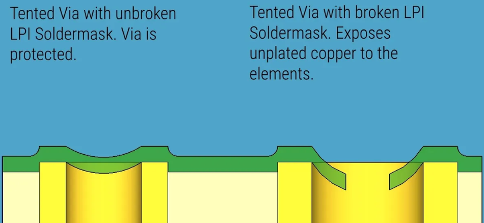
Filling reduces the chances of air or liquid getting trapped in the via holes, which can eventually lead to failure of the PCB. In many ways, filling is pretty similar to via tenting, a cost-effective method to prevent contaminants from degrading PCB performance over time. It’s just that filling doesn’t involve the removal of via solder mask pad from the PCB design.
Image source: Via Tenting for PCBA Design (wevolver.com)
Filled vias can be of several types including:
Copper-filled vias - provide better electrical conductivity
Conductive Polymer filled vias - suited for enhanced thermal conductivity
Non-conductive filled vias - Used to prevent contaminants and dirt from clogging the holes
All via types can be converted into filled vias and have several benefits such as:
They ensure tighter BGA patches.
Vias reduce electromagnetic interference (EMI).
Reduce board size by facilitating multiple layer connections.
Increase heat dissipation and enhance electrical conductivity.
Reduced layer count or board size, which translates to overall cost reduction
Further Reading: Filled Vias: A Comprehensive Guide
Key Material and Dimension Considerations
The strategic selection of materials and the precise calibration of dimensions in via design are critical for optimizing performance and reliability in modern printed circuit boards (PCBs). As electronic devices become increasingly miniaturized and complex, the demands on via technology grow, necessitating a deeper understanding of material properties and dimensional constraints.
Materials Used for Vias
Copper remains the preferred choice for most PCB applications due to its superior electrical conductivity and thermal resistance. However, alternatives like aluminum and tungsten are considered for their unique benefits such as lower cost or higher mechanical strength.
The selection often hinges on specific design criteria including environmental resistance, manufacturing ease, and compatibility with other PCB components, which can significantly influence the final product's performance and durability.
Impact of Material Properties
Impedance and Capacitance - Materials with higher conductivity, such as copper, effectively reduce impedance and maintain signal integrity, especially crucial in high-frequency applications.
Reliability - The ability of a material to withstand high temperatures and corrosive manufacturing processes is vital for the long-term reliability of the PCBs.
Influence of Via Dimensions
In the race to pack more functionality into smaller devices, the dimensions of vias play a pivotal role. Smaller vias are increasingly common in compact device designs, demanding precision in drilling and plating to avoid issues like increased resistance and signal loss.
Signal Integrity - The challenge with smaller vias is maintaining the integrity of signals—they must be carefully designed to prevent loss and interference, which are more pronounced as via diameters decrease.
Crosstalk - Proper spacing and alignment are essential to mitigate crosstalk in densely packed vias, with design strategies often tailored to the specific needs of the device architecture.
Comparative Table of Materials and Dimensions
Material | Conductivity | Cost | Impedance | Reliability | Preferred Applications |
Copper | High | Moderate | Low | High | General Electronics |
Aluminum | Medium | Low | Medium | Medium | Consumer Electronics |
Tungsten | Low | High | High | Very High | High Durability Needs |
This enhanced table now includes preferred applications, providing clearer guidance on when and why each material might be chosen based on specific electronic requirements. Understanding these factors allows engineers to design more effective and innovative PCBs, meeting the evolving challenges of electronic device manufacturing.
Recommended Reading: Mastering PCB Testing: Techniques, Methods, and Best Practices Unveiled
Advancing Technology: Recent Innovations in Via Types
Via manufacturing and design has undergone several advancements that enhance PCB performance and reliability These innovations are not only refining the functionality of traditional vias and pave the way for new capabilities in the electronics industry.
High-Density Interconnect
Recent advancements include High-Density Interconnect (HDI) technology, which facilitates faster signal transmission and greater miniaturization of devices by allowing a much higher density of vias on a PCB. It’s a crucial technology for the development of devices with increasingly complex circuitry, such as smartphones and wearable technology.
Via-In-Pad Design
The via-in-pad process is another notable innovation, where vias are placed directly within the pad structures to improve board reliability by reducing the thermal stress on critical solder joints.
Image source: PCB Directory
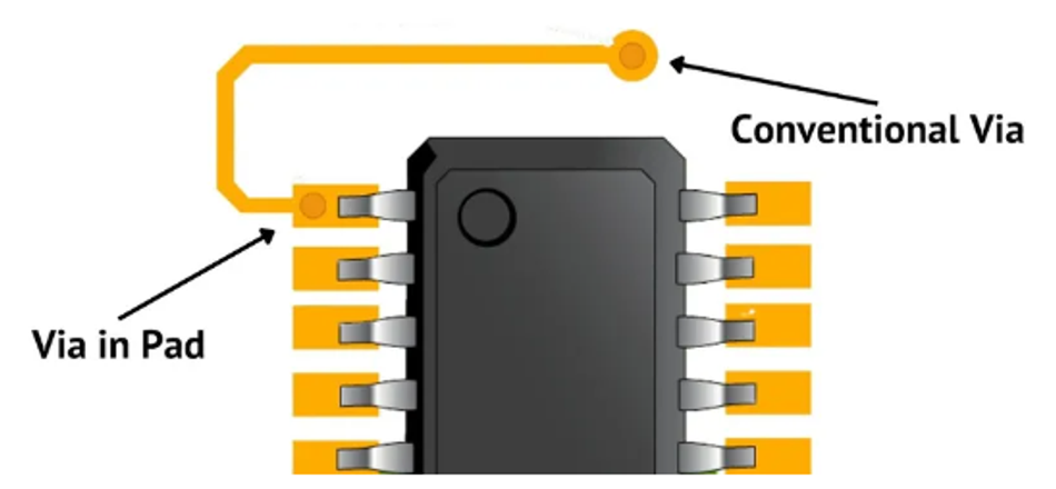
This method has seen significant application in high-performance computing and military electronics, where durability and reliability are paramount
Further Reading: Via in Pad PCB Design
Conductive Polymer for Via Filling
The introduction of conductive polymers for via fill has improved conductivity and environmental resistance compared to traditional solder materials. These polymers enhance vias' mechanical integrity and contribute to manufacturing processes' environmental sustainability by reducing reliance on lead-based solders.
Microvia Technology
Microvias are a further development characterized by their tiny size and ability to be drilled with lasers or mechanically to connect multiple layers in a PCB. Employed predominantly in stacked via architectures, microvias are integral to sophisticated, high-density electronic applications, enabling compact designs without compromising performance.
Benefits of Tech Innovations in Via Technology
Innovative via technologies are revolutionizing the design of modern circuit boards, directly addressing the challenges of miniaturization and high-speed data processing in the electronics industry.
Increased Circuit Density
Technologies like micro vias and via-in-pad designs allow for tighter component packaging, which is critical in smartphones and wearables, where space is at a premium and functionality cannot be compromised. By reducing the space required for vias, engineers can incorporate more features into smaller devices, enhancing their appeal and utility.
Faster Signal Transmission
Utilizing High-Density Interconnect (HDI) technology and smaller vias reduces the trace length for electrical signals, thus decreasing delay and increasing the speed of communication within devices. This improvement is vital in sectors like telecommunications, where rapid signal processing is fundamental to device performance.
Noise Reduction in High-Frequency Circuits
As vias directly impact the circuit size, they become a useful option in high-frequency circuits, where they offer multiple benefits such as:
Improved Signal Integrity - Advanced via solutions mitigate electromagnetic interference and crosstalk in densely packed circuits, crucial for maintaining the accuracy of high-speed data.
Enhanced Thermal Management - Conductive via fill materials not only improve electrical performance but also aid in dissipating the heat generated by high-speed electronic operations, which is vital for maintaining system stability and longevity.
Navigating Challenges: Limitations and Considerations in Via Design
Designing and implementing various via types presents significant challenges that impact the cost, manufacturing process, and reliability of printed circuit boards (PCBs).
Cost Implications
Advanced via technologies such as microvias or via-in-pad require specialized equipment and precise processes. These processes require more production costs because they involve laser drilling and precise plating techniques.
Manufacturing Complexities
The precision required for creating advanced vias adds layers of complexity to the manufacturing process. Misalignment or incomplete filling can lead to failures in connections, which may not be immediately apparent but can cause long-term reliability issues.
Reliability Concerns
As the dimensions of vias shrink and their density on PCBs increases, ensuring consistent quality and performance becomes increasingly challenging. This is particularly critical in high-stake applications such as aerospace or medical devices, where failure rates must be near zero.
Suggested Reading: PCBA Cost and Complexity Design Factors You Should Know
Thermal Management Challenges and Solutions
Effective thermal management is essential, especially as device operation speeds increase and components are packed more densely. Thermal vias play a crucial role in dissipating heat away from critical components to prevent overheating and ensure stable operation.
Real-World Example - In server farms and high-performance computing systems, thermal management is critical due to the high heat generated by dense configurations of fast-operating processors. Thermal vias are strategically placed to facilitate effective heat transfer, thus preventing thermal throttling and extending the lifespan of the hardware.
These challenges not only affect the technical aspects of PCB design but also have broader implications on product development cycles and the overall electronics manufacturing industry. Overcoming these obstacles through innovative design and manufacturing techniques is key to advancing the capabilities and reliability of modern electronic devices.
Conclusion
In this exploration of via types, the article uncovered different via types including blind, through-hole, buried, skip, and staggered vias. Each type is tailored for specific roles in modern electronics. Material choices and dimensions significantly impact attributes like impedance and signal integrity, crucial for reliability in circuit designs. Advancements such as HDI technology and via-in-pad processes have notably boosted circuit density and speed, addressing challenges like noise reduction in high-frequency circuits. This dynamic evolution underscores the importance of understanding via complexities for engineers pushing electronic design boundaries. Ongoing research promises even greater integration and performance enhancements, shaping the future of electronics.
Frequently Asked Questions About Via Types
Q1: What are the most common challenges when designing with microvias in high-density interconnect (HDI) applications?
The primary challenges include ensuring adequate reliability under thermal stress, managing cost due to more complex manufacturing processes, and handling signal integrity issues due to closer via proximity. Advanced design techniques and materials are continually being developed to address these concerns.
Q2: How do via-in-pad processes improve PCB performance, and what are the potential drawbacks?
Via-in-pad processes enhance performance by reducing the signal path length, thus lowering inductance and improving signal integrity. However, they can increase the cost of PCB manufacturing and complicate the refilling process with non-conductive or conductive epoxy to avoid solder flow into the vias during assembly.
Q3: In terms of thermal management, how do vias contribute to heat dissipation in power-intensive designs?
Vias can improve thermal management by conducting heat away from hot components towards cooler areas of the PCB or out of the PCB entirely. Designing with thermal vias often involves strategically placing these vias under heat-generating components and using materials that enhance thermal conductivity.
Q4: What are some emerging technologies in via design that could significantly impact future PCB designs?
Emerging technologies include 3D stacked vias, which offer improved space utilization and faster data transfer between layers, and conductive nano-fillers for microvias that promise better electrical and thermal performance. These innovations could revolutionize how compact and efficient future PCBs are designed.
Q5: Can you provide troubleshooting tips for signal integrity issues related to via implementation?
Troubleshooting signal integrity involves examining the via placement relative to other components, ensuring that impedance matching is correctly managed, and minimizing crosstalk with adequate spacing and shielding techniques. Simulation tools can be instrumental in identifying and mitigating potential issues before the final production.
References
Different Types of PCB Via - Through-hole, Blind, Buried, Micro Vias (flux.ai)
Difference between Via Tenting, Via Filling and Via Plugging (qualiecocircuits.com.au)
Blind Via PCB-What Should You Know(Latest introduction) (ourpcb.com)
Understanding Blind, Buried, and Through-hole vias in PCB (circuitdigest.com)
in this article
1. Introduction2. Understanding the Basics of Via Types?3. What are Filled Vias?4. Key Material and Dimension Considerations5. Advancing Technology: Recent Innovations in Via Types6. Benefits of Tech Innovations in Via Technology 7. Navigating Challenges: Limitations and Considerations in Via Design8. Conclusion9. Frequently Asked Questions About Via Types10. References