How to Read Electrical Schematics: A Comprehensive Guide for Engineers
Master the language of electronics by learning to interpret schematic diagrams, from basic symbols and conventions to complex circuit analysis.

29 Apr, 2025. 21 minutes read
Key Takeaways:
Understand the critical role of schematics as the universal blueprint in electronics design, manufacturing, and troubleshooting.
Learn to identify standard electronic component symbols (IEC & ANSI/IEEE) and interpret their meanings within a circuit context.
Master schematic layout conventions, including signal flow direction, power/ground distribution, reference designators, and net labeling.
Develop systematic strategies for analyzing schematics: identifying functional blocks, tracing signal paths, and understanding component values and ratings.
Gain practical experience by walking through schematic examples of common circuit types (digital logic, analog amplifiers, power supplies, microcontrollers).
Introduction
Electrical schematics are the universal language of electronics. They serve as blueprints that guide every stage from initial concept to final maintenance. These diagrams provide a visual representation of electrical components and their intricate interconnections. For designers and engineers, understanding how to read electrical schematics is not just a useful skill; but it represents a fundamental competency for professionals involved with electronic systems. These diagrams are essential to the lifecycle of an electronic circuits, such as:
Design
Manufacturing
Assembly
Troubleshooting
Documentation
Without proficiency in schematic literacy, navigating the complexities of modern electronics becomes an almost insurmountable challenge. Schematics are the crucial bridge, translating conceptual electronic designs into tangible physical realities. This article provides a comprehensive technical guide meticulously crafted to equip digital design engineers, hardware engineers, and electronics engineering students with the necessary knowledge and systematic methodology to read and interpret electrical schematics confidently.
The Role of Blueprints in Electrical Design
The importance of electrical schematics permeates every phase of an electronic product's lifecycle. Their mastery is not just beneficial but often mandatory for effective engineering practice, acting as the common thread connecting diverse activities and disciplines within the field.
Design & Development
Schematics are the initial blueprints for electronic systems, which:
Define logical structure and component connectivity
Enable visualization and optimization before physical construction
This visualization is vital for planning and iterative refinement. The schematic dictates electrical interactions, forming the basis for the subsequent PCB layout.
The schematic's logical design is intrinsically linked to the PCB layout's physical implementation. Schematics define the necessary connections (nets) that must be realized as physical traces, requiring corresponding layout adjustments for any schematic modifications. Hence, it requires a working knowledge of both schematic capture and PCB layout.
Suggested Reading: How to Design a PCB Layout: A Comprehensive Guide
Manufacturing & Assembly
Beyond the design phase, schematics are critical in guiding the manufacturing and assembly processes. Schematics show how the circuit components are interconnected. These are typically accompanied by a detailed Bill of Materials (BOM), which lists all required components, often including manufacturer part numbers and specifications.
Reference designators (e.g., R1, C2, U3) printed on the schematic correspond directly to labels on the PCB silkscreen. It ensures that the components are correctly placed and oriented during assembly. While schematics focus on logical connections, wiring diagrams provide more explicit physical connection details essential for manual assembly or harnessing.
Troubleshooting & Maintenance
Schematics are highly valuable when circuits malfunction. They work as a diagnostic tool, providing a clear map of the circuit's intended structure and signal paths. It allows technicians and engineers to:
Systematically trace faults
Identify malfunctioning components
Perform repairs with accuracy and efficiency
By comparing expected behavior (as depicted in the schematic) with actual measurements (voltages, waveforms), troubleshooters can isolate the source of the problem. The ability to conceptually understand system flow, learned through schematic study, is fundamental to rapid fault finding, even when specific diagrams are unavailable.
Communication & Documentation
Schematics function as a standardized, universal language within the electronics industry. Regardless of the reader’s linguistic and geographical constraints, they are readable as a common visual language. So, it enhances communication and collaboration among diverse teams, including designers, layout engineers, test technicians, and manufacturers.
Furthermore, schematics are a critical part of a project's documentation, providing a lasting record of the design intent, component choices, and connection topology. It’s essential for future reference, modifications, upgrades, and ensuring the long-term maintainability and integrity of the electronic system. Features like revision history blocks within schematic documents track changes over the product's lifecycle.
Standard Schematic Symbols
Graphical symbols help circuit readers to read schematics. These symbols represent various electronic components and functions. However, to make these symbols consistent worldwide, their standardization was crucial.
Hence, several bodies have developed standards for electronic symbols. The two most influential are:
IEC 60617: Maintained by the International Electrotechnical Commission, this is the prevailing international standard. It's a comprehensive database of graphical symbols used across electrical and electronic diagrams, aiming for global uniformity.29 Access typically requires a subscription.
ANSI/IEEE 315-1975: Developed by the American National Standards Institute and the Institute of Electrical and Electronics Engineers, this standard was dominant in North America for decades. Although officially withdrawn and no longer updated, its influence persists, particularly in legacy documentation and many modern ECAD (Electronic Computer-Aided Design) software libraries.
Additionally, ASME Y14.44-2008 often works in conjunction with IEEE 315, particularly regarding reference designators.19 The IPC-2612-1 standard specifically addresses symbol creation within modern EDA environments.
While these standards provide a framework, variations can still exist due to legacy practices, regional differences, or specific CAD tool libraries. Therefore, while memorizing standard symbols is essential, the ability to infer component function from context—analyzing connections, surrounding circuitry, reference designators, and consulting datasheets—remains a vital skill when encountering unfamiliar representations. The reference designator often serves as a primary clue to the component type.
Suggested Reading: Circuit Symbols: A Comprehensive Guide for Electronics Engineers
Passive Components (Resistors, Capacitors, Inductors)
Resistors: The ANSI/IEEE symbol for a resistor is a zigzag line, while the IEC standard uses a rectangle. Variable resistors, such as potentiometers (three terminals) and rheostats (two or three terminals used as variable), are indicated by an arrow drawn through or pointing to the basic symbol. Specialized types like photoresistors (LDRs) and thermistors also have distinct symbols. The standard reference designator is R.
Capacitors: The basic symbol consists of two parallel lines or plates. For polarized capacitors, one plate is often drawn curved, or a '+' sign is added to indicate the positive terminal. Variable capacitors, used for tuning circuits, feature an arrow passing through the plates. The reference designator is C.
Inductors: Inductor symbols typically depict a coil of wire, shown as a series of loops or a semicircle. A magnetic core (iron, ferrite) may be indicated by parallel lines drawn alongside the coil symbol (common in the IEEE standard). The reference designator is L.
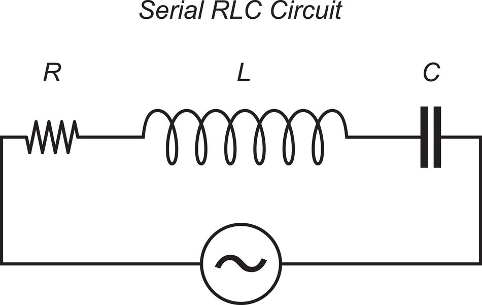 Fig 1: Standard R, L, C symbols shown in a series RLC circuit
Active Components (Diodes, Transistors, ICs)
Diodes: The basic diode symbol is a triangle (anode) pointing towards a perpendicular line (cathode).Specific types have variations: Zener diodes (used for voltage regulation) have a bent cathode line; Schottky diodes (low voltage drop) have curved ends on the cathode line; Light Emitting Diodes (LEDs) add arrows pointing away from the symbol; Photodiodes (light-sensitive) add arrows pointing towards the symbol.
Suggested Reading: Diode Symbols: A Comprehensive Guide to Understanding Circuit Diagrams
Transistors: Bipolar Junction Transistors (BJTs) are shown with connections for Base (B), Collector (C), and Emitter (E). An arrow on the emitter indicates conventional current direction and distinguishes NPN (arrow out) from PNP (arrow in) types. Field-Effect Transistors (FETs), including JFETs and MOSFETs, show connections for Gate (G), Drain (D), and Source (S). Common reference designators for transistors are Q or sometimes T.
Integrated Circuits (ICs): These complex devices contain numerous transistors, resistors, and capacitors within a single package. They are typically represented on schematics as simple rectangles or squares with numbered pins extending from the sides. The pins on the schematic symbol are often grouped by function (e.g., power, control, data bus) for clarity, which may not correspond to the physical pin arrangement on the actual chip package. The common reference designator is U or sometimes I. Therefore, understanding the pin functions requires consulting the component's datasheet.
Power Sources and Ground
Power Sources: Provide the electrical energy for the circuit. DC voltage sources are often shown as a circle with '+' and '-' polarity marks, or using the battery symbol. A battery symbol consists of alternating long (positive) and short (negative) parallel lines; multiple pairs represent a multi-cell battery.AC voltage sources are typically represented by a circle containing a sine wave symbol. Reference designators might include BT (Battery), V, G (Generator), or PS (Power Supply).
Ground (GND): Represents the common reference point in a circuit, typically considered 0 Volts. Several symbols are used: three horizontal lines of decreasing length forming a downward-pointing triangle shape is common for signal or chassis ground; an earth ground symbol (resembling a rake pointing down) indicates a connection to the physical earth, primarily for safety.
Control and Connection
Switches: Used to make, break, or redirect electrical connections. Symbols depict the switching mechanism. Common switch types include SPST (Single Pole Single Throw - simple on/off), SPDT (Single Pole Double Throw - changeover), DPST (Double Pole Single Throw), DPDT (Double Pole Double Throw), and momentary pushbutton switches (Normally Open - NO, or Normally Closed - NC). Reference designators are typically S, SW, or PB (Pushbutton).
Relays: These are electrically operated switches. The symbol shows the coil (which activates the relay when energized) and the associated switch contacts (which open or close when the relay is activated). Reference designators include K or RL.
Connectors: Provide points for connecting the circuit to external devices, wires, or other boards. Symbols vary greatly depending on the type (e.g., jack, plug, header pins, D-sub). Reference designators J (for Jacks or fixed connectors) and P (for Plugs or movable connectors) are common, as is CON.
Terminals: Specific points intended for connection, often represented by simple circles or dedicated symbols.
Logic Gates
These are the building blocks of digital circuits. Each gate performs a basic Boolean logic function on its inputs to produce an output. Standard distinctive shapes are widely used:
AND: D-shaped symbol; output is HIGH (1) only if all inputs are HIGH.
OR: Curved input side, pointed output; output is HIGH if at least one input is HIGH.
NOT (Inverter): Triangle pointing to a small circle (bubble); output is the opposite logic state of the input.
NAND (NOT-AND): AND shape with an output bubble; output is LOW (0) only if all inputs are HIGH.
NOR (NOT-OR): OR shape with an output bubble; output is HIGH only if all inputs are LOW.
XOR (Exclusive-OR): OR shape with an additional curved line on the input side; output is HIGH if the inputs are different.
XNOR (Exclusive-NOR): XOR shape with an output bubble; output is HIGH if the inputs are the same. The IEEE standard also defines rectangular symbols with internal notations for logic functions, though the distinctive shapes are more common in many contexts.
Suggested Reading: How to Read a Circuit Board: Mastering the Language of Electronics
Understanding Schematic Layout Conventions
Beyond individual symbols, the way components and connections are arranged on a schematic follows established conventions designed to ensure clarity and readability.
Signal Flow (Left-to-Right, Top-to-Bottom)
Schematics generally use a left-to-right convention for signal flow (inputs on the left, outputs on the right) and a top-to-bottom convention for power (higher voltages at the top, ground at the bottom). It’s much like reading text and helps in circuit comprehension. Feedback signals, an exception, flow right-to-left and are often emphasized visually.
Power and Ground Distribution
Consistent representation of power and ground is vital for clarity. Power supply symbols (VCC, VDD, +5V, etc.) are conventionally drawn pointing upwards, while ground symbols (GND, VSS, 0V) point downwards. Instead of drawing long, crossing wires for power distribution, designers use dedicated power and ground symbols connected by named nets.
In PCB design, power and ground are often distributed using large copper areas called planes, especially in multi-layer boards. These planes provide low-impedance paths for current return, improve signal integrity, aid thermal management, and provide shielding.
Reference Designators (REFDES)
As previously introduced, reference designators are unique alphanumeric codes assigned to every individual component on the schematic (e.g., R1, R102, C5, U7A). They are fundamental for:
Uniqueness: Each component has one unique REFDES.
Identification: The letter prefix indicates the component type (based on standards like IEEE 315 / ASME Y14.44).
Linking: They connect the schematic symbol to its corresponding entry in the Bill of Materials (BOM) and its physical footprint/location on the PCB layout.
Communication: They provide an unambiguous way to refer to specific components during design reviews, testing, and troubleshooting.
Table 1: Common Reference Designator Prefixes (ASME Y14.44 / IEEE 315)
Prefix Letter(s) | Component Type |
R | Resistor |
C | Capacitor |
L | Inductor |
D, CR | Diode (General, Rectifier) |
Z, ZD, VR | Zener Diode |
Q, T | Transistor (BJT, FET, etc.) |
U, IC | Integrated Circuit |
J | Jack, Receptacle, Connector (Fixed) |
P | Plug, Connector (Movable) |
S, SW, PB | Switch, Pushbutton |
F | Fuse |
Y, X, XTAL, OSC | Crystal, Oscillator, Resonator |
K, RL | Relay, Contactor |
BT, BAT | Battery |
TP | Test Point |
FB | Ferrite Bead |
DS, LED | Display, Lamp, LED |
M | Motor |
MK, MIC | Microphone |
LS, SPK | Loudspeaker, Buzzer |
T, TR | Transformer |
FL | Filter |
AT | Attenuator |
CB | Circuit Breaker |
CN | Capacitor Network |
RN | Resistor Network |
HY | Circulator, Directional Coupler |
VR | Voltage Regulator (sometimes U) |
W | Wire, Cable |
X | Socket, Holder (e.g., XF for Fuse) |
Nets, Net Names, and Labels
The lines drawn between component pins represent electrical connections, known as nets.4 In anything beyond the simplest circuits, drawing every single connection can lead to a cluttered and unreadable diagram, often referred to as a "rat's nest". To avoid this, designers assign net names (also called net labels) to identify connections logically.
Placing a net label (e.g., DATA0, SPI_MOSI, +3V3_ANALOG, /RESET) on a wire segment assigns that name to the entire electrical node. All wire segments and component pins connected to points bearing the same net name are considered electrically connected, even if there isn't a continuous line drawn between them on the schematic.
Effective net naming follows conventions for clarity:
Names are often written in uppercase.
Active-low signals (asserted when the voltage is low) are commonly indicated with a prefix like '/', '!', '#', or a suffix like '_L', '_N', or an overbar if the tool supports it.
Bus signals (groups of related signals like data or address lines) often share a common prefix followed by a number (e.g., ADDR..ADDR1 or DATA0, DATA1,...).
It's good practice to name all nets, even if the name seems trivial, to aid in debugging and netlist verification.
Junctions, Nodes, and Connections
How connecting wires are depicted is critical to avoid ambiguity:
Junctions/Nodes: A solid dot placed at the intersection of two or more crossing wires explicitly indicates an electrical connection at that point.
Crossings (No Connection): Wires that cross on the schematic but do not have a dot at the intersection are not electrically connected; they are merely passing over each other on the drawing.
Avoiding Ambiguity: A common best practice is to avoid having four wires meet at a single junction point (a '+' shape). Instead, connections should be staggered using two T-junctions.
Jumps/Bridges: Some schematic styles or tools use a small arc or "jump" where one wire crosses another without connecting.
A Systematic Approach to Reading Schematics
Reading a schematic effectively, especially a complex one, requires more than just recognizing symbols.
Schematic Overview
Start with the schematic’s title block. You can do it by examining the title block for project metadata (name, title, sheet number, revision, date, designer). Review the initial page for a high-level block diagram showing major subsystems and their interaction. Next, check for introductory notes, legends, or a revision history explaining design choices and standards.
Locate Major Functional Blocks
Next, you need to break down the schematic into logical functional sections (e.g., Power Supply, Input Conditioning, Processing Core, Memory Interfaces, Output Drivers, Connectors). Well-organized schematics group these blocks, aiding in understanding the overall architecture.
Locate Power Supply Sections
Identify primary power inputs and trace the flow through voltage regulation stages to determine voltage rails (e.g., +12V, +5V, +3.3V, -5V) and ground connections. Observe power and ground distribution using symbols and net labels. Note decoupling capacitors near integrated circuit power pins.
Trace Signal Paths
Follow key signals from inputs (e.g., sensors, connectors, switches) through components (amplifiers, filters, logic gates, microcontrollers), observing signal modification. Continue to outputs (e.g., actuators, displays, connectors). Use consistent net names to track connections across sheets.
Interpret Component Values, Tolerances, and Ratings
Note nominal values (e.g., R1: 10kΩ, C3: 0.1μF, D1: 1N4148) crucial for circuit behavior. Understand capacitor shorthand (e.g., "104" = 100 nF). Note tolerance (e.g., ±5%) indicating permissible deviation, often via letter codes or resistor color bands. Recognize standard E-series values for resistors and capacitors. Pay attention to maximum voltage and power ratings to prevent component damage.
Practical Examples: Reading Different Circuit Types
Applying the systematic approach to concrete examples solidifies understanding. Let's explore how to interpret schematics for common circuit categories relevant to digital design engineers, hardware engineers, and students.
Digital Logic Circuits
Digital circuits operate using discrete voltage levels, typically representing binary logic states (0/LOW, 1/HIGH). Reading their schematics involves:
Identifying Gates: Recognize the standard symbols for basic logic gates (AND, OR, NOT, NAND, NOR, XOR, XNOR) and understand their corresponding Boolean functions and truth tables.
Tracing Logic Flow: Follow signal paths from inputs, through combinational logic (gates connected), to outputs. Determine the logic state at each gate's output based on the states of its inputs.
Sequential Elements: Identify flip-flops (D-type, T-type, JK-type) or latches, which introduce memory into the circuit. Note their clock inputs (often marked with a triangle) and understand how they capture or change state based on the clock signal and data/control inputs.
Bus Notation: Recognize thicker lines or grouped net names (e.g., DATA[7..0]) representing buses, which carry multiple related signals.
Support Components: Note pull-up or pull-down resistors, often used to define a default logic state for inputs or open-drain outputs.
Analog Circuits (Op-Amp Amplifiers)
Analog circuits process continuous signals. Operational amplifiers (Op-Amps) are ubiquitous building blocks. Reading Op-Amp schematics involves:
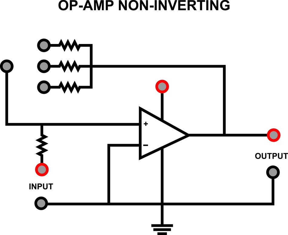
Identifying the Op-Amp: Recognize the triangular symbol with two inputs (inverting '-' and non-inverting '+') and one output. Note the power supply connections (e.g., +Vcc, -Vee, or GND), which are sometimes omitted from the main symbol for clarity but are crucial for operation.
Recognizing Topologies: Identify common configurations based on where the input signal is applied and how the feedback network (usually resistors, sometimes capacitors) connects the output to the inputs. Key topologies include:
Inverting Amplifier (Input to '-', '+' to reference/GND, feedback resistor from output to '-')
Non-inverting Amplifier (Input to '+', feedback network from output to '-')
Voltage Follower (Output connected directly to '-', input to '+')
Summing Amplifier (Multiple inputs through resistors to '-')
Differential Amplifier (Inputs to both '+' and '-')
Applying Ideal Op-Amp Rules (for initial analysis):
No current flows into the input terminals (infinite input impedance).
The voltage difference between the '+' and '-' inputs is zero when negative feedback is present (infinite open-loop gain forces inputs to be equal).
Calculating Gain: Use the ideal rules and basic circuit analysis (like Kirchhoff's laws or nodal analysis) to determine the circuit's gain, which is typically set by the ratio of external resistors. For an ideal inverting amplifier, the Voltage Gain (Av) = -Rf / Rin, where Rf is the feedback resistor and Rin is the input resistor.
Power Supply Circuits (Linear & SMPS)
Power supplies convert an input voltage (AC or DC) to the required DC voltage(s) for the circuit.
Linear Regulators: These are simpler but often less efficient. Identify the regulator IC (e.g., 7805 for +5V) or discrete components (pass transistor, Zener reference). Look for input and output capacitors, essential for stability and filtering ripple. Trace the input voltage, regulated output voltage, and ground connections.
Switch Mode Power Supplies (SMPS): These are more complex but highly efficient. Reading SMPS schematics involves identifying key functional blocks and components :
Input Stage: AC input usually goes through an EMI filter (inductors, capacitors) and a bridge rectifier to produce high-voltage DC, stored in a large bulk capacitor. DC input might bypass the rectifier.
Switching Stage: Identify the main switching element (MOSFET or BJT) and the core topology based on the arrangement of the switch, inductor (L), diode (D), and output capacitor (C).
Buck (Step-Down): Switch in series with inductor.
Boost (Step-Up): Inductor in series with input, switch shunts inductor to ground.
Buck-Boost (Inverting): Topology varies, often involves switch followed by inductor to ground.
Output Stage: Includes the output rectifier diode (often a fast Schottky diode) and the output filter capacitor(s) to smooth the switched voltage into DC.
Control Circuit: Usually an integrated circuit (SMPS controller) that generates the Pulse Width Modulated (PWM) signal to drive the switch.
Feedback Path: Senses the output voltage and compares it to a reference, adjusting the PWM duty cycle to maintain regulation. This path often includes an optoisolator for safety isolation between the high-voltage primary side and the low-voltage secondary side.
Isolation: In AC-DC supplies, look for the transformer that provides galvanic isolation between the mains input and the output.
Suggested Reading: Linear vs Switching Power Supply: Understanding the Differences
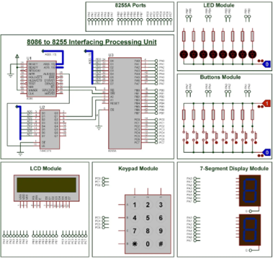
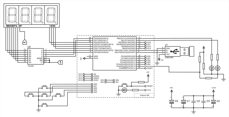
Microcontroller Systems (Arduino Example)
Microcontrollers (MCUs) are the programmable brains of many embedded systems. Reading an MCU system schematic involves tracing connections to its various peripherals and support circuitry. Using the Arduino Uno as an example:
Core MCU: Identify the main microcontroller chip (e.g., ATmega328P).
Power: Locate the power input options (USB port, DC barrel jack, VIN pin) and the onboard voltage regulators (typically 5V and 3.3V) that supply power to the MCU and other components. Note the power source selection circuitry (often using MOSFETs) if multiple sources are possible.
Clock: Find the crystal oscillator or ceramic resonator connected to the MCU's clock input pins, which determines the operating speed.
Programming/Debugging: Identify the programming header (e.g., ICSP - In-Circuit Serial Programming) used for flashing firmware.
Reset Circuit: Locate the reset button and associated circuitry connected to the MCU's reset pin.
I/O Pins: Trace connections from the MCU's GPIO (General Purpose Input/Output) pins to the physical headers on the board. Note which pins have special functions like Analog-to-Digital Conversion (ADC inputs, often labeled A0, A1...), Pulse Width Modulation (PWM outputs, often marked with '~'), or hardware communication interfaces.
Communication Interfaces:
USB: Since many MCUs lack native USB, look for a dedicated USB-to-Serial (UART) bridge chip (e.g., ATmega16U2 on the Uno) connecting the USB port to the main MCU's UART pins (RX/TX). Note associated components like termination resistors and ESD protection.
Serial (UART): Identify the RX (Receive) and TX (Transmit) pins, often shared with digital I/O pins (e.g., D0, D1 on Uno).
SPI (Serial Peripheral Interface): Locate the MOSI (Master Out Slave In), MISO (Master In Slave Out), SCK (Serial Clock), and SS (Slave Select) pins.
I2C (Inter-Integrated Circuit): Find the SDA (Serial Data) and SCL (Serial Clock) pins.
Suggested Reading: I2C vs SPI vs UART: A Comprehensive Comparison
The Key to Handling Complex Diagrams
Modern electronic systems often result in large, intricate schematics that can be challenging to interpret. Employing specific strategies and adhering to best practices can significantly ease the process of understanding complex, multi-page, or hierarchical designs.
Handling Multi-Page Schematics
As designs grow, they inevitably exceed the space of a single sheet. Strategies for navigating these include:
Inter-Sheet Connections: Signals that continue from one page to another are connected logically using off-page connectors or, more commonly, net labels. An off-page connector symbol typically includes the net name and often references the page number and grid location where the signal continues. Using identical net labels on different sheets implies a connection.
Top Sheet/Block Diagram: Well-structured multi-page schematics often include a top sheet that acts as a high-level block diagram. This sheet shows symbols representing the other schematic sheets (often called sheet symbols) and the major signals or buses connecting them, providing an overview of the system architecture.
Consistent Naming: Clear and consistent net naming across all pages is critical for accurately tracing signals that span multiple sheets.
Understanding Hierarchical Designs
Hierarchical design is a powerful technique for organizing very complex schematics, often used in conjunction with multi-page layouts.
Structure: A higher-level schematic sheet contains sheet symbols, which are blocks representing entire sub-circuits detailed on separate, lower-level schematic sheets. This creates a tree-like structure.
Navigation: Readers can understand the system architecture from the top level and then "descend" into specific functional blocks (sheet symbols) to examine their detailed circuitry.
Ports: Connections between hierarchy levels are made using ports placed on the lower-level schematic sheet, which correspond to sheet entries on the sheet symbol in the higher-level sheet.
Common Errors in Handling Schematics
Awareness of common mistakes helps avoid misinterpretations:
Symbol Errors: Misinterpreting non-standard symbols or confusing visually similar ones (e.g., different types of ground, polarized vs. non-polarized capacitors).
Connection Errors: Missing connection dots at junctions, assuming a connection where wires merely cross, or misinterpreting ambiguous 4-way junctions.
Ignoring Context: Analyzing a component in isolation without considering its role in the surrounding circuit or the overall signal flow direction.
Layout Assumptions: Incorrectly assuming the schematic directly represents the physical size, placement, or routing of components on the PCB.
Verification Lapses: Failing to double-check connections, component values, or pin numbers against datasheets.
Power/Ground Issues: Overlooking missing decoupling capacitors, incorrect voltage connections, or inadequate ground paths.
Rushing: Trying to analyze a complex schematic too quickly, leading to missed details.
Suggested Reading: What Are Schematics: The Blueprint Language of Engineering Decoded
Tools and Resources for Schematic Interpretation
Efficiently reading and working with schematics is greatly aided by modern software tools and readily available documentation resources.
Schematic Capture and Viewing Software
These software packages, also known as EDA (Electronic Design Automation) or ECAD (Electronic Computer-Aided Design) tools, are used to create, view, analyze, and manage schematic diagrams and their associated data (like netlists and BOMs). Altium Designer: A high-end, integrated platform for professional PCB design, offering comprehensive features from schematic capture to simulation and collaboration. It's powerful but expensive with a steeper learning curve.
Autodesk Eagle: A widely used, affordable (with free options) tool popular among hobbyists and small businesses, integrating with Fusion 360. While capable, it lacks some advanced features and can be less intuitive for some users.
KiCad: A powerful, free, and open-source EDA suite for schematic capture, PCB layout, and basic simulation, rivaling commercial options. It benefits from strong community support but has limited official support and may require more manual library management.
OrCAD (Cadence): A professional-grade suite known for its robust PSpice simulation and advanced analysis, integrating with Allegro for complex designs. It's a costly and complex solution suited for experienced users
Leveraging Datasheets and Application Notes
Component datasheets are indispensable resources for correctly interpreting schematics and understanding circuit behavior.12 They provide authoritative information directly from the manufacturer, including:
Detailed electrical specifications (voltage/current ratings, timing, logic levels).
Pin configurations (pinouts) and functional descriptions for each pin.
Absolute maximum ratings (conditions beyond which damage may occur).
Recommended operating conditions.
Typical performance characteristics (often shown in graphs).
Functional block diagrams of the component's internal structure.
Physical dimensions and packaging information.
Example application circuits.
Relevant Standards Documents
For definitive information on symbols and reference designators, consulting the original standards documents is ideal, although access may require purchase or subscription:
IEC 60617: The international standard for graphical symbols (subscription required).
IEEE 315-1975: The foundational North American standard for symbols and class designation letters (officially inactive but still referenced).
ASME Y14.44-2008: The current standard for reference designations, replacing IEEE 200.
Conclusion
The ability to interpret electrical schematics is fundamental to electrical and electronics engineering, acting as a universal language and essential blueprint throughout the electronic product lifecycle, from initial design to maintenance. This guide has explored the core principles of schematic literacy, encompassing the standardized symbols from major international standards and critical layout conventions like signal flow, power distribution, reference designators, and net naming, all of which ensure clarity and broad comprehension. A systematic approach to reading schematics was presented, emphasizing the necessity of gaining a holistic understanding, identifying functional units, tracing the pathways of power and signals, and meticulously interpreting component specifications.
Practical examples illustrated these principles across various circuit types, including digital, analog, power, and microcontroller systems. The guide also addressed the complexities of multi-page and hierarchical schematics, providing strategies for effective navigation and error prevention. Furthermore, it highlighted the importance of utilizing schematic capture software and essential resources like component datasheets. Ultimately, mastering schematic interpretation is a dynamic skill crucial for effective communication, collaboration, systematic problem-solving, and innovation in the ever-evolving field of electronics, demanding continuous practice and the utilization of available tools.
FAQ Section
1. What's the difference between a schematic and a wiring diagram?
A schematic diagram illustrates the logical connections and functionality of components in a circuit using standardized symbols, focusing on how the circuit works electrically. A wiring diagram, conversely, depicts the physical layout and actual wire connections between components, often showing their relative positions and how they should be physically assembled or wired. Schematics prioritize electrical function, while wiring diagrams prioritize physical construction.
2. Why are there different symbols for the same component (e.g., resistor)?
Different symbols often exist due to the evolution of standards and regional preferences. The two most common standards are IEC 60617 (international, often uses rectangles for passives) and ANSI/IEEE 315 (historically North American, often uses zigzag lines for resistors). Legacy drawings or specific industries might also use older or specialized symbols.
3. What does a dot at a wire intersection mean? What if wires cross without a dot?
A solid dot placed where wires intersect signifies an electrical connection or junction; the wires are connected at that point. If wires cross on the schematic without a dot at the intersection, it indicates that there is no electrical connection between them; they are simply passing over each other in the drawing.
4. How do I follow a signal that goes off one page and onto another?
Look for special symbols called off-page connectors or simply matching net names (labels) on the different sheets. Off-page connectors typically show the net name and often include a reference to the page number and sometimes grid coordinates where the signal continues. If net labels are used, find the identical net name on the other sheet(s); all points with the same net label are electrically connected.
5. What's the best way to start reading a complex, multi-page schematic?
Begin by examining the title block on each page and looking for a top-level block diagram or an overview page if available. Identify the main functional blocks or modules represented on different pages. Choose a key section to focus on first (e.g., power input, main processor, a specific interface). Trace the primary inputs and outputs for that block, using net names or off-page connectors to understand its interaction with other blocks before diving into the detailed circuitry within the block.
6. What does a reference designator like 'U5' or 'R12' mean?
A reference designator (REFDES) is a unique identifier assigned to each component on the schematic. The letter(s) typically indicate the type of component ('U' for Integrated Circuit, 'R' for Resistor), and the number distinguishes that specific component from others of the same type (e.g., R12 is the twelfth resistor in the design sequence).
7. Where can I find the exact part number for a component shown on a schematic?
The exact manufacturer part number (MPN) for a component identified by a reference designator (e.g., R12) is found in the Bill of Materials (BOM) document associated with the schematic. The BOM lists all components required for the design, linking the REFDES to specific part numbers, quantities, descriptions, and sometimes supplier information.
References
Top 10 PCB Design Software Tools for Engineers in 2025 - ALLPCB, accessed on April 9, 2025, https://www.allpcb.com/blog/pcb-design/top-10-pcb-design-software-tools.html
Electrical Schematics: The Blueprint for Electrical Systems - Medium, accessed on April 9, 2025, https://medium.com/@harshhvm/electrical-schematics-the-blueprint-for-electrical-systems-1951054a2bfa
The Role of Schematic diagram in Electronics Industry - CompileIoT, accessed on April 9, 2025, https://compileiot.online/the-role-of-schematic-diagram-in-electronics-industry/
Understanding the Essentials of a Circuit Diagram: A Comprehensive Guide - Zuken, accessed on April 9, 2025, https://www.zuken.com/us/blog/understanding-the-essentials-of-a-circuit-diagram-a-comprehensive-guide/
Schematic Design Rules | Sierra Circuits, accessed on April 9, 2025, https://www.protoexpress.com/kb/schematic-design-rules/
Understanding and Using Electronic Diagrams - Workforce Development, accessed on April 9, 2025, https://www.workforcedevelopment.com/pdf/sample/Sample_Lesson_Understanding_and_Using_Electronic_Diagrams.pdf
How to Read Electrical Schematics - Circuit Basics, accessed on April 9, 2025, https://www.circuitbasics.com/how-to-read-schematics/
How to Read a Schematic - SparkFun Learn, accessed on April 9, 2025, https://learn.sparkfun.com/tutorials/how-to-read-a-schematic/all
Understanding Schematics - Technical Articles - All About Circuits, accessed on April 9, 2025, https://www.allaboutcircuits.com/technical-articles/understanding-schematics/
The Ultimate Guide to Schematic & BOM Formation - PCB Runner, accessed on April 9, 2025, https://www.pcbrunner.com/schematic-bom-formation/
PCB Schematic Design: Essential Tips and Best Practices - PCBTok, accessed on April 9, 2025, https://www.pcbtok.com/pcb-schematic-design/
Top 5 Do's and Dont's of PCB Design Schematic Capture - Gighz, accessed on April 9, 2025, https://gighz.net/ecad/top-5-dos-and-donts-of-pcb-design-schematic-capture/
Graphic Symbols for Electrical and Electronics Diagrams - EE IIT Bombay, accessed on April 9, 2025, https://www.ee.iitb.ac.in/~spilab/Tips/ansii_graphic_symbols_for_electrical_and_electronics_daigrams_1993.pdf
IEEE STANDARD SYMBOLS - Wakerly's, accessed on April 9, 2025, http://wakerly.org/DDPP/DDPP3_pdf/IEEEsyms.pdf
IEEE/ANSI 315-1975 - IEEE Standards Association, accessed on April 9, 2025, https://standards.ieee.org/standard/315-1975.html
Which standard dictates how reference designations should be formed in the EU?, accessed on April 9, 2025, https://electronics.stackexchange.com/questions/22956/which-standard-dictates-how-reference-designations-should-be-formed-in-the-eu
Electrical Symbols Guide.pdf, accessed on April 9, 2025, https://www.reconelectrical.co.uk/image/data/pdfs/Electrical%20Symbols%20Guide.pdf
Basic Schematic Symbols - Electronics Tutorials, accessed on April 9, 2025, https://www.electronics-tutorials.ws/resources/basic-schematic-symbols.html
SCHEMATIC GENERATION RULES AND CONVENTIONS, accessed on April 9, 2025, https://littlebluecad.tripod.com/sch_guid.html
How to read a schematic - Soldered Electronics, accessed on April 9, 2025, https://soldered.com/learn/how-to-read-a-schematic/
How to draw schematics: the good, the bad, and the ugly. | by Tiago Gala | Medium, accessed on April 9, 2025, https://medium.com/@tiago.gala/the-art-of-drawing-good-schematics-be3e7e59eb40
Electrical Symbols and Line Diagrams, accessed on April 9, 2025, https://abe.ufl.edu/faculty/tburks/Presentations/ABE5152/Electrical%20Symbols%20and%20Line%20Diagrams.pdf
IEC Symbols (IEC 60617) | Capital X Panel Designer by Siemens, accessed on April 9, 2025, https://symbols.radicasoftware.com/225/iec-symbols
Ultimate Guide To PCB Schematics - Jhdpcb, accessed on April 9, 2025, https://jhdpcb.com/blog/ultimate-guide-to-pcb-schematics/
Electrical Symbols IEEE Std 315-1975, Quick Reference Only - iProcesSmart.com, accessed on April 9, 2025, https://www.iprocessmart.com/techsmart/elecsymbols.htm
Step-by-step guide: How to read and create circuit diagrams - SMART ENGINEERS, accessed on April 9, 2025, https://smartengineers.com/en/stromlaufplan-lesen-erstellen-anleitung/
Interpreting Electrical Schematics - LunchBox Sessions, accessed on April 9, 2025, https://www.lunchboxsessions.com/materials/interpreting-electrical-schematics/interpreting-electrical-schematics-lesson
High-Speed PCB Design Guide - S3VI, accessed on April 9, 2025, https://s3vi.ndc.nasa.gov/ssri-kb/static/resources/High-Speed%20PCB%20Design%20Guide.pdf
Circuit Board Layout Guide: 10 Steps for Success - 911EDA, accessed on April 9, 2025, https://www.911eda.com/news/circuit-board-layout-guide/
Schematic and Netlist Checks for Error-Free PCBs - Sierra Circuits, accessed on April 9, 2025, https://www.protoexpress.com/blog/schematic-and-netlist-checks-ensure-error-free-designs/
8 Best Electronic Circuit Design Practices | Sierra Circuits, accessed on April 9, 2025, https://www.protoexpress.com/blog/best-electronic-circuit-design-practices/
Circuit Simplification Examples | Boolean Algebra | Electronics ..., accessed on April 9, 2025, https://www.allaboutcircuits.com/textbook/digital/chpt-7/circuit-simplification-examples/
Introducing the Microcontroller + Arduino : 17 Steps - Instructables, accessed on April 9, 2025, https://www.instructables.com/Introducing-the-Microcontroller-Arduino/
Arduino Uno Schematic Diagram: A Comprehensive Guide - Flux, accessed on April 9, 2025, https://www.flux.ai/p/blog/arduino-uno-schematic-diagram
Advantages of Hierarchical Block Diagrams and Schematic Designs for PCB Schematic Layouts - Altium Resources, accessed on April 9, 2025, https://resources.altium.com/p/how-hierarchical-schematic-design-can-help-your-next-pcb-schematic-layout
Reading a Data Sheet - Screaming Circuits, accessed on April 9, 2025, https://www.screamingcircuits.com/resource-center/tips/reading-data-sheet
in this article
1. Key Takeaways:2. Introduction3. The Role of Blueprints in Electrical Design 4. Standard Schematic Symbols5. Understanding Schematic Layout Conventions6. A Systematic Approach to Reading Schematics7. Practical Examples: Reading Different Circuit Types8. The Key to Handling Complex Diagrams9. Tools and Resources for Schematic Interpretation10. Conclusion11. FAQ Section