Calculate Impedance in AC Circuits: A Comprehensive Guide for Engineers
Learn how to calculate impedance in AC circuits – from basic RLC components to complex transmission lines and PCB traces. This guide covers the theory, formulas, methods, and tools needed to determine impedance accurately and ensure proper impedance matching in their designs.

22 Apr, 2025. 19 minutes read
Key Takeaways:
Impedance Basics: Impedance (Z) is the total opposition a circuit offers to AC, combining resistance (R) and reactance (X) into a complex quantity (Z = R + jX). Unlike pure resistance, impedance depends on frequency and has both magnitude and phase.
Components’ Impedances: Resistors have constant impedance (R), inductor impedance increases with frequency (Z_L = jωL), and capacitor impedance decreases with frequency (Z_C = 1/(jωC)).
Impedance Calculation Methods: You can calculate impedance using Ohm’s Law in the AC domain (V = I·Z) and phasor algebra. Impedances add in series and combine as reciprocals in parallel.
High-Speed Considerations: In high-frequency designs, characteristic impedance of transmission lines (e.g. ~50 Ω for many signal lines ) and controlled impedance PCB traces (microstrip, stripline) must be calculated and maintained to avoid signal reflections.
Tools & Best Practices: Engineers use LCR meters and impedance analyzers for low-frequency impedance measurements, and vector network analyzers (VNAs) for high-frequency impedance characterization. Other simulation tools like (SPICE) can predict impedance versus frequency, and good measurement practices.
Introduction
Impedance is a fundamental concept in electronics that every hardware engineer encounters. Whether it’s about low-frequency circuits like audio amplifiers, switching power supplies, or high-speed digital PCBs, impedance calculation is a critical design aspect required at different points of a circuit.
Therefore, understanding how to find and calculate the impedance of a complex RLC network helps in filter design, and determining the impedance of a PCB trace is critical for impedance matching in high-speed signal links. Essentially, impedance extends the idea of simple resistance to AC circuits by including the effects of capacitors and inductors, whose opposition to current varies with frequency.

What is impedance?
Impedance is the total opposition a circuit presents to alternating current. It is measured in ohms (Ω), just like resistance. However, unlike pure resistance, which applies to DC or steady-state current, impedance in AC circuits includes reactance – the frequency-dependent opposition from inductors and capacitors.
Impedance is a complex quantity with a magnitude and a phase angle. Therefore, it can be expressed as a combination of a real part (resistance R) and an imaginary part (reactance X) . Therefore, calculating impedance involves not just the size of the opposition but also the phase relationship between voltage and current.
In practice, calculating impedance lets engineers predict how AC circuits will behave: it lets them determine the current draw for a given AC voltage (using AC Ohm’s law I = V/Z), find resonance points, and design matching networks.
This article provides a comprehensive tutorial on how to calculate impedance in various scenarios. It will cover:
Theoretical background of impedance, phasors, and reactance.
Methods for calculating the impedance of different components and circuit combinations.
Special cases of transmission line impedance (characteristic impedance) and PCB trace impedance for high-speed designs.
Practical tools (like VNAs and impedance analyzers) and techniques for measuring or simulating impedance will be covered.
Understanding Impedance in AC Circuits (Resistance, Reactance, and Phasors)
In a DC circuit, we deal only with resistance, a measure of how much a component opposes steady current. In AC circuits, however, we encounter reactance alongside resistance. Reactance arises from energy storage elements: inductors and capacitors “resist” changes in current or voltage, respectively.
Resistance vs. Reactance
A resistor’s impedance is purely real and equal to its resistance R. It does not depend on frequency and causes no phase shift between voltage and current. On the other hand, an inductor and a capacitor have a purely imaginary impedance that varies with frequency:
An inductor with inductance L has an impedance:
Zl=jωL
The term jωL(where j is the imaginary unit and ω=2πfis angular frequency) indicates a positive imaginary impedance, meaning the voltage leads the current by 90° in an inductor. The magnitude of the inductive reactance is XL=ωLX_L, which increases linearly with frequency f. At higher frequencies, an inductor offers a larger opposition to AC (open circuit for very high frequencies), while at DC (f = 0, ω=0\omega=0) an ideal inductor’s impedance is zero (a short circuit).
A capacitor with capacitance C has an impedance
Zc=− j/ωC.
This is a negative imaginary quantity, indicating capacitor voltage lags the current by 90°. The magnitude of the capacitive reactance is XC=1/ωCwhich decreases as frequency increases. At high frequencies, a capacitor’s impedance approaches zero (short circuit), whereas at very low frequencies or DC, its impedance is extremely high (open circuit).
Suggested Reading: Open Circuit vs Short Circuit: Core Differences between Open and Closed Circuit
A purely resistive impedance can be thought of as
Z=R+j0(zero imaginary part),
An ideal pure reactance is
Z=0±jX(zero real part). Most real circuits have some combination of both.

Impedance as a Complex Number
We combine resistance and reactance into a single complex expression for impedance:
Z=R+jX,
where
R is the real part (resistive component),
X is the imaginary part (reactive component, positive for inductive, negative for capacitive).
Ohm’s Law and Phasors
Ohm’s Law generalizes to AC circuits using impedance: V=I⋅Z. If we treat the sinusoidal voltage V and current I as phasors (complex representations of their amplitude and phase), their ratio yields the complex impedance Z.
Therefore, you can calculate impedance by taking the phasor voltage divided by the phasor current at a given frequency. The phase angle of impedance equals the voltage phase minus the current phase.
A phasor diagram is a helpful visual tool: it’s a rotating vector diagram that shows the relative phase of voltages and currents.
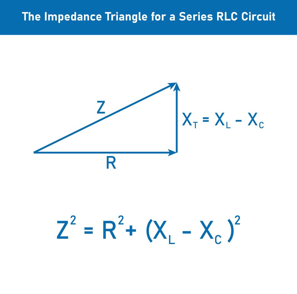
For example, in a series circuit with a resistor and an inductor, the resistor’s voltage drop is in phase with the current, while the inductor’s voltage drop is 90° ahead of the current. Drawing these as perpendicular vectors (resistive voltage on the horizontal axis, inductive on the vertical) yields a right triangle; the hypotenuse represents the total voltage (and thus total impedance times current).
Frequency Dependence
Impedance is generally a function of frequency. Resistive elements are constant, but inductive and capacitive reactances vary with frequency. Thus, the impedance of an RLC network can change dramatically over the frequency spectrum – for instance, at a certain frequency, the inductive and capacitive reactances might cancel each other (resonance), yielding a purely resistive impedance. So, it’s important to specify the frequency while determining the impedance of reactive circuits.
Suggested Reading: Types of Circuits: A Comprehensive Guide for Engineering Professionals
Calculating Impedance of Basic Components (R, L, and C)
To calculate the impedance in any AC circuit, a good starting point is knowing the impedance of the individual components at the operating frequency. Here we summarize the impedance formulas for resistors, inductors, and capacitors:
Component | Impedance (Z) | Behavior (Phase) |
Resistor (R) | ZR=R (purely real) | Voltage and current in phase (0° phase difference). |
Inductor (L) | ZL=j ωL | Voltage leads current by +90°. |
Capacitor (C) | ZC=− j/ωC | Voltage lags current by –90°. |
These relations tell us how to find impedance for each type of passive element:
Resistors: Impedance is simply equal to the resistance (e.g., a 10 Ω resistor has Z = 10 + j0 Ω at all frequencies). There is no frequency dependence or phase shift introduced by an ideal resistor.
Suggested Reading: Resistor Chart: Comprehensive Guide to Resistor Values, E-Series, and Color Codes
Inductors: Impedance grows with frequency. For example, a 1 mH inductor has XL=2πf⋅0.001. At f = 1 kHz, XL≈6.28 Ω; at 100 kHz, XL≈628 Ω. The j in ZL=jXL signifies a +90° phase (current lags voltage). Inductors impede high-frequency currents more than low-frequency currents.
Capacitors: Impedance diminishes with frequency. For a 1 µF capacitor, XC=1/(2πf⋅10−6). At f = 1 kHz, XC≈159 Ω; at 100 kHz, XC≈1.59 Ω. The –j indicates a –90° phase (current leads voltage). Capacitors pass high-frequency AC more easily (low impedance) while blocking low-frequency or DC (high impedance).
Suggested Reading: PCB Components: A Comprehensive Technical Guide to Passive, Active, and Electromechanical Parts
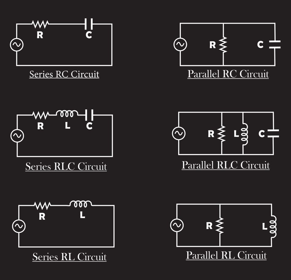
Impedance in Series and Parallel Circuits
Most practical circuits have multiple components. To calculate the impedance of a network, you’ll often need to combine the impedances of components in series or parallel. The combination rules are analogous to those for resistors, just using complex arithmetic:
Series Impedances
Impedances in series simply add up. If an inductor (Zl) is in series with a resistor (R) and a capacitor (Zc), the total impedance is
Ztotal=R+ZL+ZC
Ztotal=R+jωL+1/jωC.
You add the real parts and imaginary parts separately. For example, a series R–L circuit has:
Z=R+jXL
a series R–C has
Z=R−jXC
a series R–L–C would be
Z=R+j(XL−XC)
If XL=XC at some frequency, the imaginary parts cancel and the impedance becomes purely R (this is the resonance condition in a series RLC).
Parallel Impedances
Impedances in parallel combine like resistors in parallel using reciprocals (admittances). The equivalent impedance Z_eq of N parallel impedances Z1, Z2, ... ZN is given by:
1Zeq=1Z1+1Z2+⋯+1ZN.
For two impedances in parallel, a convenient formula is:
Zeq=Z1Z2/(Z1+Z2)
which is analogous to the product-over-sum for two resistors. Keep in mind Z’s are complex, so the algebra involves complex multiplication and addition.
Series–Parallel Combinations
Many circuits can be reduced by first combining some elements in series and others in parallel step by step. For instance, in a series-parallel RLC network, you might combine series components into a partial impedance, then compute the parallel with another branch, etc. The process is the same as you learned for resistive circuits, except you use complex arithmetic. It can be helpful to break the problem: first compute the impedance of each branch, then combine those branches in parallel or series as needed. If the math gets cumbersome, a phasor-domain circuit simulator or a tool like SPICE (more on that later) can compute it for you.
Phasor Diagram for Series vs. Parallel
In a series circuit, the same current flows through each element, and phasor voltages add. In a parallel circuit, the same voltage is across each branch, and phasor currents add.
But in both cases, the method to calculate equivalent impedance is to use the series sum or parallel reciprocal formula. Always pay attention to signs of reactive components (jX for inductor, –jX for capacitor) when adding.
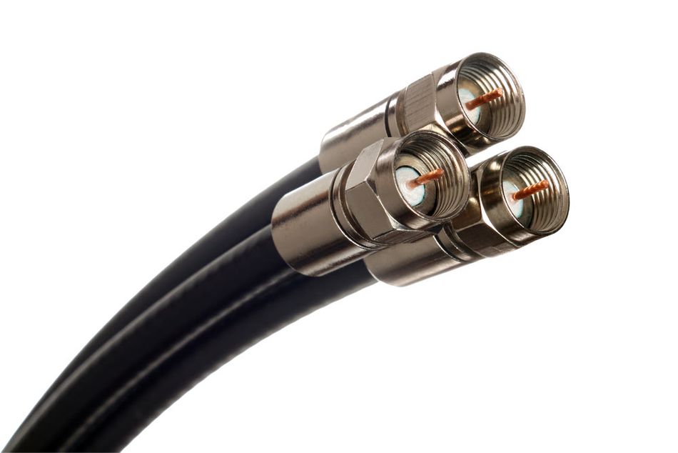
Characteristic Impedance of Transmission Lines
When dealing with high-frequency signals or fast digital edges, circuit traces and cables must be treated as transmission lines. A transmission line (like a coaxial cable or a PCB trace routed over a ground plane) has a property called characteristic impedance, usually denoted Z₀.
This is the impedance that the line presents to a wave traveling along it, independent of the line’s length (assuming the line is either infinitely long or properly terminated such that there are no reflections). In essence, if you send a fast signal into a long cable, it will appear as if the cable is a resistor of value Z₀ as far as that signal is concerned.
Definition: Characteristic impedance (also known as surge impedance) is the ratio of voltage to current of a single propagating wave on the line, in the absence of reflections. For a lossless (or low-loss) transmission line, Z₀ is determined by the geometry and materials of the line:
For a coaxial cable, Z0=L′C′, where L' and C' are inductance and capacitance per unit length. Standard coax cables often have Z₀ of 50 Ω or 75 Ω by design.
For parallel wire lines or PCB traces, Z₀ is given by more complex formulas depending on conductor spacing, trace width, dielectric constant, etc. For example, a parallel two-wire line’s impedance can be approximated by Z0=276 log10(D/r)εr, where D is the spacing, r is the wire radius, and εr is the dielectric constant. Microstrip and stripline have their own empirically derived formulas or can be found via calculators.
Suggested Reading: PCB Trace: The Backbone of Modern Circuit Design
It’s important to note that the characteristic impedance is frequency-dependent when losses and dielectric dispersion are considered, but in the ideal lossless case, it can be treated as constant over a range. Typical high-speed digital and RF systems use lines with a controlled Z₀ (50 Ω is most common, but others like 75 Ω for video, 100 Ω differential for Ethernet/USB, etc., are used).
Calculating or Determining Z₀
Unlike a simple lumped impedance, you usually don’t calculate a trace’s characteristic impedance from scratch with basic algebra; instead, you use field solver tools, impedance calculators, or standardized formulas.
For instance, a microstrip (trace over a ground plane) impedance depends on trace width, trace thickness, dielectric constant (εr) of the PCB material, and the height of the trace above the plane. There are online calculators and PCB design tools that output Z₀ when you input those parameters.
As a quick sense: a 50 Ω microstrip on FR-4 (~εr = 4.3) might have a width on the order of twice the height above the plane (this is very rough; actual formula is nonlinear). A stripline (trace buried between planes) will have a different formula and typically narrower width for the same impedance due to the dielectric above and below.
Example: Suppose you have a 50 Ω coax cable and you connect it to an antenna that has 50 Ω impedance – this is a matched condition, and the transmitter will see a 50 Ω load. If the antenna were 200 Ω, the mismatch would cause much of the power to reflect back down the line (poor transfer). Engineers use impedance matching techniques to adjust the effective impedance and achieve 50 Ω. In high-speed digital PCBs, if a trace that’s supposed to be 50 Ω is routed incorrectly and ends up 80 Ω, when the fast edge travels, it will partially reflect at impedance discontinuities, causing ringing in the measured waveform.
Suggested Reading: Fab Insights: A Practical Guide to Impedance Control & High-Speed Routing
PCB Trace Impedance (Microstrip and Stripline Calculations)
On printed circuit boards, the concept of characteristic impedance translates to traces acting as transmission lines. There are two common types of PCB transmission line structures:
Microstrip: A trace on an outer layer of the PCB, separated from a reference plane (ground or power plane) by a dielectric. One side of the trace “sees” air (or solder mask), the other sees substrate.
Stripline: A trace sandwiched between two reference planes inside the PCB (completely embedded in dielectric).
Both have well-defined formulas for impedance. For a simplistic understanding:
The microstrip impedance depends on trace width (W), dielectric thickness (H, the distance to the plane), dielectric constant (ε_r), and trace thickness (T). Narrower traces, thinner dielectric (closer plane), or higher ε_r all result in lower impedance (because capacitance per length is higher). Wider traces or lower ε_r give higher impedance.
The stripline impedance depends on similar factors, but since the field is fully in the dielectric, the equations differ. Generally, for the same geometry, a stripline yields a lower impedance than a microstrip (because the field is confined and the effective dielectric constant is higher).
In practice, designers often target specific impedances for certain signals. For example, USB, HDMI, and PCIe differential pairs are typically routed as 90 Ω differential (which corresponds to two 50 Ω single-ended traces in a pair) . A single-ended clock or RF trace might be 50 Ω. The actual calculation of PCB trace impedance is done either by:
Consulting standards or manufacturer data: PCB fabs often provide impedance tables or will adjust the width for you if you specify the target impedance and layer buildup.
Using software tools: CAD tools like Altium Designer, KiCad (with plugins), or specialized tools (Polar Instruments’ Si9000, ATLC, etc.) can compute impedance. Even general resources like everyday calculators or online tools are available where you enter W, H, T, ε_r and get Z₀ .
Building a field solver model: For critical designs, a 2D field solver can give accurate impedance considering all geometry details.
Practical Tools and Techniques for Impedance Measurement and Simulation
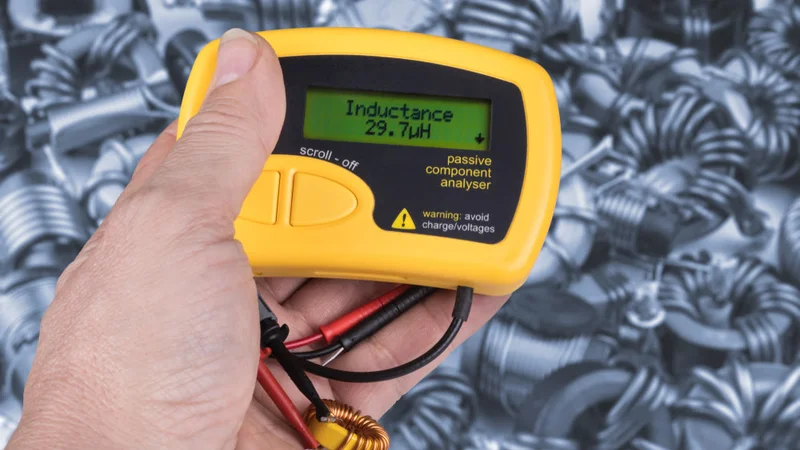
Thus far we’ve discussed how to calculate impedance on paper. In practice, engineers often verify impedance through measurements or simulations. This section covers common tools: impedance analyzers, vector network analyzers, LCR meters, SPICE simulations, and best practices for accurate impedance measurements.
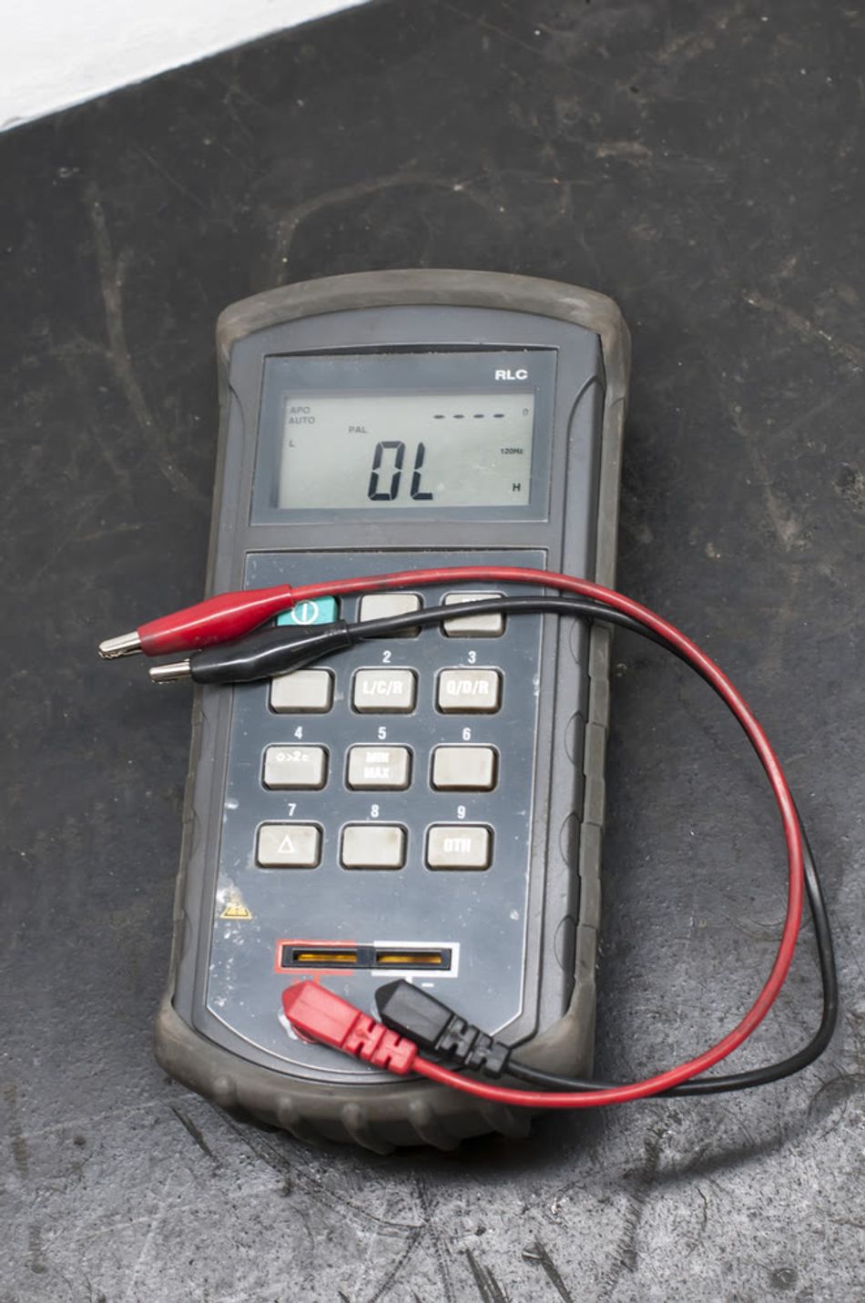
Impedance Analyzers and LCR Meters vs. VNAs
For low to mid frequencies (from DC up to maybe low MHz or a few tens of MHz), dedicated impedance analyzers or LCR meters are used to measure impedance of components and circuits. These instruments apply a small AC signal to the Device Under Test (DUT) and measure the resulting current and phase to compute impedance directly (often providing results in terms of magnitude/phase or equivalent R and X).
They can often sweep frequency to produce an impedance vs. frequency curve. A typical LCR meter might measure from 20 Hz to 1 MHz, for example, and can auto-select ranges to measure impedances from milliohms to megaohms. They often support 4-wire (Kelvin) connections to eliminate lead resistance for low impedance measurements.
For high frequencies (RF and microwave, from kHz up to GHz), the tool of choice is the Vector Network Analyzer (VNA). A VNA measures scattering parameters (S-parameters), essentially looking at reflected and transmitted signals when a known reference impedance (usually 50 Ω) is connected. From S-parameters, the complex impedance can be calculated.
VNAs typically have ports with 50 Ω characteristic impedance; by measuring S11 (reflection coefficient at the port), the VNA can compute the impedance of the DUT using calibration and conversion formulas. Modern VNAs can even directly display impedance or admittance on a Smith chart or vs. frequency.
Suggested Reading: Next-Generation Current Measurement: Addressing PCB Design Challenges with Magnetic Current Sensors
Simulation Tools (SPICE and Beyond)
Sometimes you want to determine impedance without physically building the circuit. Circuit simulation is invaluable for this. A common approach:
Use a SPICE-based simulator (like LTspice, PSpice, Multisim, etc.) to model your circuit.
To find impedance in SPICE, you can do an AC sweep analysis. For input impedance, a trick is to drive the circuit input with an AC current source of 1 A; then the AC voltage at that source node directly equals the impedance (since V = I·Z and I=1 A).
SPICE can output complex data, or you might have to compute magnitude and phase from real/imag parts. Some SPICE GUIs let you directly plot impedance versus frequency by proper measurement probe or scripting.
For example, to simulate the impedance of a parallel RLC circuit, you could:
Place a 1A AC source across the RLC network.
Perform an AC sweep from, say, 1 Hz to 1 MHz.
Plot the voltage across the source; that voltage at each frequency is the complex impedance (in linear analysis SPICE will give real and imag components, or you can derive magnitude = |V| since |I|=1).
The plot of |Z| vs. f might show a resonance dip or peak, etc.
Beyond SPICE, there are RF simulation tools (Keysight ADS, AWR Microwave Office) and field solvers that compute impedance of structures from Maxwell’s equations. For most circuit impedance tasks, though, SPICE is sufficient.
Measurement Best Practices and Challenges
Measuring impedance accurately in real life can be tricky. Here are some common challenges and strategies:
Parasitics: Real components are not ideal – a resistor has some small inductance and capacitance, a capacitor has equivalent series resistance (ESR) and inductance (ESL), an inductor has winding resistance and inter-winding capacitance. These parasitic elements mean the impedance of a component can deviate from the ideal formula, especially at high frequencies. For example, a capacitor might measure as capacitive at low frequency, but above its self-resonant frequency, it looks inductive (because the ESL dominates).
Mitigation: Manufacturers often provide impedance vs. frequency curves for components. When measuring, be aware of the frequency range and if possible, measure a known standard to see the system’s behavior.
Fixture and Lead Effects: The leads, wires, or PCB traces used to connect to the measuring instrument add impedance (especially inductance for leads and capacitance for fixture geometry). At high freq, even a few centimeters of wire can add a significant inductive reactance (e.g. 5 cm of test lead might be ~50 nH, which is j15 Ω at 50 MHz!).
Mitigation: Use the shortest possible leads, use 4-wire connections for low impedance (the sense leads carry almost no current so they don’t drop voltage).
Dynamic Range and Frequency Limits: An LCR meter might struggle to measure a very high impedance (e.g. 100 MΩ) or a very low one (e.g. 0.001 Ω) due to instrument limitations. Similarly, a VNA has a noise floor and might not accurately resolve an extremely high-Q impedance at certain frequencies.
Mitigation: Know your instrument’s range; for very low impedances, use instruments that can apply 4-wire kelvin and high test currents; for very high, use guarded measurements to reduce leakage.
Temperature and Bias: Impedance of components can depend on temperature or DC bias (capacitors, especially ceramics, change capacitance with applied DC voltage; inductors can saturate with DC current, altering inductance). When measuring, consider if you need a DC bias applied (some impedance analyzers have DC bias sources for measuring e.g. in-circuit capacitance under bias). Keep temperature stable or measure quickly to avoid drift.
Reflections and Cable Length (for RF): When using a VNA to measure a component at high frequency, how you mount the component matters. If it’s not directly at the calibrated plane, the intervening structure (like a fixture or PCB) will itself have a transmission line impedance and needs de-embedding. E.g., measuring a SMT capacitor might involve a test jig with a coax launch; you should calibrate up to the launch and possibly do port extension or de-embedding to get the true component impedance.
Real-World Examples and Case Studies
Let’s solidify the concepts with a couple of real-world examples:
Example 1: Impedance of a Series RLC Circuit (Resonance)
Imagine a series circuit with a resistor R = 10 Ω, an inductor L = 100 μH, and a capacitor C = 10 μF. What is the impedance at 1 kHz and at 5 kHz?
First, compute reactances:
At 1 kHz:
XL=2π(1000)(100×10−6)≈0.628 Ω
XC=1/[2π(1000)(10×10−6)]≈15.9 Ω
The net reactance X = Xl – Xc ≈ 0.628 – 15.9 = –15.27 Ω (capacitive overall).
So Z at 1kHz=10−j15.27 Ω. The magnitude |Z| = √(10^2 + 15.27^2) ≈ 18.3 Ω, and phase φ = arctan(–15.27/10) ≈ –56°. This circuit at 1 kHz is dominated by the capacitor (current leads voltage).
At 5 kHz:
XL=2π(5000)(100e−6)=3.14 Ω=. XC=1/[2π(5000)(10e−6)]=3.18 Ω
Net X ≈ 3.14 – 3.18 = –0.04 Ω (almost zero – interestingly, this is near resonance).
Z5kHz≈10−j0.04 Ω, essentially 10 Ω with a tiny capacitive part. |Z| ≈ 10.0 Ω, φ ≈ –0.23°, nearly purely resistive. Indeed, the resonant frequency of this RLC is
f0=1/(2πLC) =1/(2π100e−6⋅10e−6)≈1591 Hz.
At 5 kHz we’re past resonance in this case, but because R is small, the impedance at resonance would dip to roughly R (the resistive value). At exactly f0, XL = Xc, the reactive parts cancel, and Z = R (minimum impedance for series RLC).
Example 2: Impedance Matching a Transmission Line
Suppose you are designing a high-speed ADC input, and the manufacturer’s datasheet says the ADC analog input has an impedance of 1 kΩ. You need to drive it from a 50 Ω source over a short PCB trace. Directly connecting 50 Ω to 1 kΩ will cause a reflection because of impedance mismatch. You decide to add a series resistor at the source to match it.
Here the “transmission line” is the PCB trace, which we’ll design to 50 Ω. The source (driver op amp) likely has low output impedance (say 50 Ω or less), so by adding a series resistor Rs, we can make source+Rs = 50 Ω total. Let’s assume the op amp output is ~0 Ω for simplicity and use Rs = 50 Ω. Now the source impedance is 50 Ω, line is 50 Ω – a perfect match on the source end.
On the ADC end, we have 1 kΩ (which is much higher than 50 Ω). This is an mismatch that will cause most of the wave to be absorbed by the 1 kΩ but a small portion (reflection coefficient
Γ = (Z_load–Z0)/(Z_load+Z0) = (1000–50)/(1000+50) ≈ 0.90) to reflect. 90% reflection is actually quite high – meaning almost the entire wave reflects back. That sounds bad, but note what happens at the source: the reflected wave traveling back hits the source which is matched (50 Ω source to 50 Ω line) – at the source, the reflection sees a matched termination and is absorbed without re-reflection.
The net effect is a form of source termination: the initial signal that goes down the line is half the amplitude (voltage divider between source 50 and line 50), and when it reaches the high impedance ADC, the voltage doubles (because the energy reflects, adding to the incident wave). The ADC effectively sees the full signal amplitude but delayed by the travel time. There is no ringing because the reflection was absorbed at the source side on the second pass.
Example 3: Measuring a Component’s Impedance Profile
You have a 10 μF electrolytic capacitor and want to know its impedance across frequency (for power supply decoupling purposes). You use an impedance analyzer to sweep from 100 Hz to 1 MHz. The result might look like:
At 100 Hz, |Z| ≈ 160 Ω (mostly capacitive, phase ~ –90°).
At 1 kHz, |Z| ≈ 16 Ω.
At 10 kHz, |Z| ≈ 1.6 Ω.
At 100 kHz, |Z| has dropped to a minimum of 0.2 Ω – this is the ESR (equivalent series resistance) of the cap, and it occurs at the capacitor’s self-resonant frequency where X_C equals the ESL’s X_L. Phase is 0° here.
Beyond 100 kHz, the impedance starts rising again (inductive region now). At 1 MHz, |Z| might be 1 Ω (inductive).
Conclusion
Impedance is the cornerstone of AC circuit analysis and high-frequency design. In this article, we’ve learned that to calculate impedance we combine resistances and reactances using complex numbers, apply Ohm’s Law in phasor form, and use series/parallel combination rules to break down complex networks. We discussed how inductors and capacitors introduce frequency-dependent impedance, and how these frequency effects can lead to resonance or filtering behavior. We also explored specialized cases like transmission line characteristic impedance – a critical factor in signal integrity for fast digital and RF circuits – and how to design or measure controlled impedance on PCB traces to ensure minimal signal reflections.
As technology advances, impedance analysis remains a vital skill. In fact, with ever higher speeds in digital systems (fast edge rates equivalent to multi-GHz frequencies) and the proliferation of RF applications (5G, IoT radios, etc.), understanding impedance is more important than ever. Future trends include more automated impedance tuning (e.g., adaptive matching networks), and increasingly, simulation tools that can predict system-level impedance issues (like power distribution network impedance peaks that cause noise).
FAQs
1. What is the difference between resistance and impedance?
Resistance is the opposition to a steady DC current. It’s a real number and does not depend on frequency. On the other hand, Impedance is the opposition to AC current, consisting of resistance and reactance. Impedance is usually expressed as a complex value Z = R + jX. The main difference is that impedance includes effects of capacitors and inductors (which create reactance) and so, it varies with frequency, causing phase shifts between voltage and current. Impedance at 0 Hz (DC) is just resistance, but it may be different at other frequencies. In short, all resistors have impedance (equal to R, constant with frequency), but inductors and capacitors have impedance that changes with frequency (pure reactance in the ideal case).
2. How does frequency affect impedance?
Frequency can affect impedance in the following ways:
The impedance of an inductor increases with frequency: XL=2πfL. So at higher f, an inductor looks more like an open circuit (higher Ω). At low f (approaching DC), an ideal inductor’s impedance goes to 0 Ω, behaving like a short circuit.
The impedance of a capacitor decreases with frequency: XC=1/(2πfC). So at higher f, a capacitor allows AC to pass more easily (lower Ω). At low f (DC), a capacitor’s impedance becomes extremely high.
Complex networks can have resonant frequencies where inductive and capacitive reactances cancel out. Below resonance a circuit might look capacitive, above it inductive. Frequency can also bring out the parasitic traits of components (e.g. a capacitor’s ESL making it inductive at very high f).
3. Can I measure impedance with a multimeter?
A regular digital multimeter (DMM) typically measures DC resistance when you use the ohmmeter function – it applies a small DC (or low-frequency) signal to estimate resistance. It does not directly measure AC impedance as a function of frequency. To truly measure impedance (magnitude and phase) across frequencies, you would need an LCR meter or impedance analyzer, which can sweep a range of AC frequencies and measure the response.
4. Why is impedance matching important?
Impedance matching ensures that the source impedance, transmission line impedance, and load impedance are equal. It is crucial for several reasons, such as:
Maximum Power Transfer: If you want to deliver the most power from a source to a load.
Signal Integrity: In high-speed digital signals, if the impedance of the transmission line and load aren’t matched to the driver, reflections can occur, causing voltage overshoot, ringing, or even logical errors.
Minimizing SWR in RF lines: In RF transmission lines, a mismatch causes a standing wave pattern due to reflections, quantified by the standing wave ratio (SWR). A high SWR means less forward power and more losses/heat in the system.
Avoiding distortion: Reflections can distort analog signals (for instance, in audio or video cables, mismatches can cause frequency response issues). In practical terms, if you connect a 50 Ω RF source to a 50 Ω cable and a 50 Ω load, you get a clean transfer. If the load were 100 Ω, a significant part of the wave would reflect back.
5. How do I calculate PCB trace impedance?
Calculating the impedance of a PCB trace (microstrip or stripline) usually involves using empirically derived formulas or software tools – it’s not as simple as a single algebraic equation like for a resistor. The impedance depends on the trace geometry and PCB materials:
For a microstrip (trace on outer layer): key parameters are trace width (W), thickness (T), height above ground plane (H, the dielectric thickness), and dielectric constant (ε_r) of the substrate. Hammerstad and Jensen’s equations are used for calculation, which typically takes these parameters and outputs Z₀.
For a stripline (internal trace between planes), the parameters are trace width, thickness, dielectric constant, and the distances to planes above/below. The formula is different from that of a microstrip and typically yields lower impedance for the same width because it’s fully in dielectric. In practice, you would use an impedance calculator – many PCB design tools have one, or you can use online tools.
6. Why is impedance expressed as a complex number (what does the j mean)?
Impedance is expressed as a complex number Z=R+jX to capture the two-dimensional nature of AC opposition – magnitude and phase. The j (imaginary unit) signifies a 90° phase shift. A positive imaginary part (+jX) means an inductive effect (voltage leads current), and a negative imaginary part (–jX) means a capacitive effect (voltage lags current). Using complex numbers allows engineers to use algebraic techniques to solve AC circuits with sinusoidal sources, by treating resistances and reactances in one unified framework.
References
in this article
1. Introduction2. Understanding Impedance in AC Circuits (Resistance, Reactance, and Phasors)3. Calculating Impedance of Basic Components (R, L, and C)4. Impedance in Series and Parallel Circuits5. Characteristic Impedance of Transmission Lines6. PCB Trace Impedance (Microstrip and Stripline Calculations)7. Practical Tools and Techniques for Impedance Measurement and Simulation8. Real-World Examples and Case Studies9. Conclusion10. FAQs11. References