How Do QFN Packages Compare to Other Surface Mount ICs?
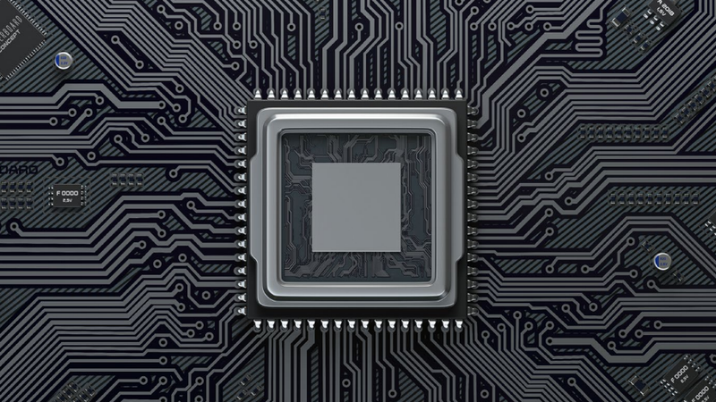
QFN packages are leadless and have short interconnects that reduce parasitic elements such as inductance and capacitance. How do they compare to other surface-mount ICs?
16 Feb, 2024. 9 minutes read
QFN
This article was first published on
www.macrofab.comThe advent of the Quad Flat Pack No Leads (QFN), a leadless packaging method, is revolutionizing the landscape of printed circuit board assembly (PCBA). Its rapid adoption can be attributed to its cost-effectiveness, minimal stand-off height, which paves the way for slender end-products, and its outstanding thermal and electrical characteristics.
However, integrating a new package style always introduces new challenges and learning curves, especially for those in the board design and manufacturing domains.
This article aims to arm electrical engineers and PCBA designers with comprehensive insights into the QFN package. We will explore its comparison with other package types and help you select the optimal QFN package for your PCBA projects. This will equip you to better utilize the full potential of this innovative packaging solution.
Leadless Package Style
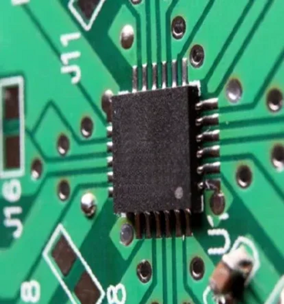
Leadless package styles refer to integrated circuits (ICs) lacking extending wires, commonly known as ‘leads,’ ‘pins,’ or ‘legs.’ These packages differ from traditional ICs that employ external leads for electrical connections. Instead, leadless packages establish connections to the printed circuit board through contact pads positioned on their underside. Hence, they are also known as bottom termination components (BTCs).
| Advantages of leadless package | Advantages of leaded packages |
|---|---|
| Compact size: Leadless packages, by design, occupy less space on the PCBA, which is essential for high-density designs. | Easy to solder: Leaded packages have leads that are easier to solder manually, making them more suitable for prototyping and small-scale production. |
| Enhanced performance: Shorter signal paths in leadless packages reduce signal delay and noise, offering improved electrical performance - particularly important in high-speed and high-frequency applications. | Visual inspection: Leaded packages can be more easily inspected for soldering defects because the leads are visible, which simplifies quality control processes. |
| Better thermal management: The heat generated by the IC can be conducted away more effectively in leadless packages because the heat can escape directly through the bottom of the package. | Easier rework: In case of soldering errors or component failures, leaded packages can be more easily de-soldered and replaced than leadless packages. |
| Higher I/O density: Leadless packages like BGAs can offer more interconnections in a given area than leaded packages. | Lower sensitivity to thermal stress: The leads in leaded packages can help absorb thermal expansion differences between the IC and the PCB, reducing the risk of solder joint failure. |
The main advantage of leadless packages is their compact design. The contact pads on the bottom provide a more compact form factor, reducing size and pitch. This compactness enhances performance by mitigating the potential signal integrity disruptions caused by the parasitic effects of leads.
Additionally, leadless packages excel in thermal management. The presence of bottom contact pads allows for more efficient heat dissipation, effectively conducting the generated heat away from the IC. These inherent characteristics make leadless packages highly desirable in space-constrained and in high-speed or high-frequency applications.
QFN Package Design and Structure
The QFN package is a type of near-chip scale package, a design that closely mirrors the physical dimensions of the silicon chip it houses. The lands or terminals on its bottom surface make electrical contact with the PCB, similar to other leadless packages.
A standout feature of QFN is the large heat-dissipation pad under the package. This exposed pad, alternatively referred to as the lead frame die pad or thermal pad, serves a dual purpose:
- Firstly, it effectively conducts heat away from the IC and towards the PCB, eliminating the necessity for bulky heat sinks or slugs. This not only helps in maintaining optimal IC operation but also contributes to a slimmer end-product profile.
- Secondly, the exposed thermal pad performs a crucial role in providing stable ground and robust electrical connections. This is achieved through the use of conductive die-attach material, which establishes a secure bond between the IC and the thermal pad.
Let’s take a closer look at the individual components that make up QFN’s structure:
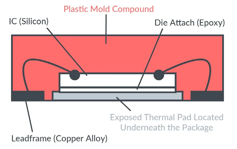
- Leadframe (Copper Alloy): The leadframe is essentially the foundation of the QFN package. Made from a copper alloy, it provides mechanical support to the package and electrical paths (leads) from the silicon IC to the external circuitry.
- Exposed Thermal Pad Located Underneath the Package: As its name suggests, the thermal pad’s primary purpose is to help dissipate heat from the IC, keeping it cool during operation. The fact that it’s exposed allows for direct contact with the PCB, enabling efficient heat transfer.
- Die Attach (Epoxy): The die-attach, typically an epoxy-based material, fastens the silicon IC (die) onto the lead frame. This conductive adhesive provides a thermal path from the IC to the thermal pad and leadframe. It’s essential for both mechanical sturdiness and thermal management.
- IC (Silicon): The IC is the heart of the package. This IC houses thousands to millions of microscopic electronic components such as transistors, resistors, and capacitors, which together execute the desired electronic function.
- Plastic Mold Compound: Finally, encapsulating these components is the plastic mold compound. This material protects the internal structure - the IC, the die attach, and part of the leadframe - from environmental conditions like moisture, dust, and physical shocks, ensuring reliable, long-term operation.
Advantages of QFN Packages in PCBA Manufacturing
QFN package design plays a vital role in PCBA manufacturing for a number of reasons:
- Space Efficiency: With electronic devices trending towards miniaturization, the compact design of QFN packages allows manufacturers to place more components on a given area of a PCB. This is crucial for densely populated boards found in small form-factor devices like wearables.
- Heat Management: The thermal performance of an electronic assembly is critical to its reliability and longevity. The QFN’s design, with its exposed thermal pad, efficiently directs heat away from the IC and toward the PCB. This helps maintain the IC within its operating temperature range, reducing the risk of thermal-induced failures.
- Electrical Performance: The leadless nature of the QFN package, with its short interconnects, aids in reducing parasitic elements like inductance and capacitance. This helps improve the electrical performance of the IC, particularly in high frequency applications.
- Cost-effectiveness: QFN packages are smaller than many other types of packages, such as Ball Grid Array (BGA) or Plastic Leaded Chip Carrier (PLCC). This means they use less material, which can significantly reduce the cost per unit. Also, QFN packages can be surface mounted to a PCB using standard reflow soldering techniques, which are generally cheaper and faster than other methods used for larger packages. This ease of assembly helps reduce manufacturing costs.
As you steer your tech company’s PCBA design decisions, QFN packages offer advantages you shouldn’t overlook.
They are small and space-efficient, ideal for today’s trend toward miniaturized electronics. They manage heat effectively and provide excellent electrical performance, ensuring reliable operation. Plus, QFN packages are cost-effective. This cost-effectiveness becomes a crucial factor in manufacturing scalability.
QFN Package Variations and Their Comparison to Other ICs
| Package Variation | Advantages | Limitations |
|---|---|---|
| MicroLeadFrame (MLF)/Quad Flat No- Lead (QFN) | Smaller size, low profile, good thermal/electrical performance | Limited I/O count, specialized rework equipment |
| Dual-row MicroLeadFrame (DRMLF) | Increased I/O count, improved electrical performance | Larger size, may require more board space |
| Advanced Quad Flat No-Lead (aQFN) | Enhanced thermal dissipation, improved electrical performance | Slightly larger footprint |
| Array Quad Flat No-Lead (Array QFN) | Higher I/O count, reduced parasitic inductance, improved electrical performance | Increased complexity in layout design, higher cost |
| Dual Flat No-Lead (DFN) | Compact size, reduced package height, improved electrical performance | Limited I/O count, higher sensitivity to thermal stress |
| No Bump Array Quad Flat No-Lead (NBA-QFN) | Improved RF performance, reduced parasitic capacitance, smaller size | Limited I/O count, higher cost compared to standard QFN |
| Thin Quad Flat No-Lead (TQFN) | Thin profile, small footprint, good thermal dissipation | Limited I/O count, increased susceptibility to mechanical stress |
| Very Thin Quad Flat No-Lead (VQFN)/ Wettable Flank Quad Flat No-Lead (WQFN) | Extremely thin profile, small size, good thermal/electrical performance | Limited I/O count, sensitive to mechanical stress during assembly |
| Land Grid Array (LGA) | High pin density, Good thermal and electrical performance | Requires high-precision assembly, Complex rework procedures |
Each of these leadless packages offers unique advantages and can be selected based on the specific requirements of the application in question.
Here is another table to get a comparative look at major IC packaging types:
Distinguishing Among Major IC Packaging Types
| Packaging Type | Structure | Advantages | Disadvantages |
|---|---|---|---|
| QFP (Quad Flat Package) | Flat package with leads (pins) on all four sides | Easy to handle and test, compatible with traditional soldering methods, visual quality control | Large footprint, limited pin density, difficult soldering with small lead pitch. |
| VQFN (Very-thin Quad Flat No-leads) | Thin package with metal pads on the underside. | Small size, thin profile, excellent thermal performance due to exposed pad. | Difficult to handle, test, and visually inspect due to hidden solder connections. |
| BGA (Ball Grid Array) | Uses solder balls on the underside for connections. | High pin density, small footprint, superior thermal and electrical performance. | Requires precise placement and reflow soldering, difficult inspection and rework due to hidden solder balls. |
| LGA (Land Grid Array) | Uses metal pads on the underside, and typically uses a socket for connection. | Supports high pin counts, IC can be replaced without desoldering. | Requires a socket (additional cost and height), connection may not be as robust as a soldered one. |
Challenges in QFN Packaging and Tips to Overcome Them
While QFN packages offer several benefits, integrating them into PCBAs may prove difficult. To ensure optimal performance, careful board design and meticulous package mounting are essential.
Here’s an overview of some common obstacles encountered when utilizing QFN packages and suggested ways to navigate them:
PCBA Design Considerations
- Thermal Pad and Via Design: The QFN package has an exposed die paddle on the bottom surface, which is vital for its superior thermal performance. To fully harness this feature, the PCB must have a thermal pad and vias to conduct heat away from the package.
- Solder Masking: The solder masking type used, whether solder mask defined (SMD) or non-solder mask defined (NSMD), can impact the reliability of solder joints. NSMD pads are usually preferred for perimeter lands as they allow the solder to wrap around the metal pads, enhancing the solder joint’s reliability. A “trench” type solder mask opening is advised for finer pitch parts when not enough space is available for a mask web between the pads.
Mounting Considerations
Proper solder joint formation is crucial for QFN packages due to the small lead surface area and the reliance on the solder paste on the PCB surface.
- Stencil Design for Perimeter Pads and Thermal Pad: To achieve reliable solder joints, the stencil aperture design must ensure full paste release. This is typically achieved by making the stencil aperture 1:1 with the PCB pad sizes. For the thermal pad, multiple smaller openings in the stencil instead of one big one can help minimize solder paste coverage and voiding for the thermal pad. Laser-cutting and electropolishing will yield the best results. Polishing smooths out stencil walls, making paste easier to release.
- Solder Voiding: Solder voiding can negatively impact high-speed RF applications and thermal performance. Solder masking may be required for the thermal vias to prevent solder wicking. Try to keep void sizes smaller than the via pitch.
- QFN Soldering Method: The recommended way to solder each package is through the reflow process. This is because, during assembly, the liquid solder buoyancy of the small pads and the surface tension of the larger heat-sink pad can create competing forces. If these forces become unbalanced, it can lead to processing defects. Also, it’s important to ensure that the temperature of the soldering does not exceed the maximum reflow temperature profile.
Rework Considerations
Reworking QFN packages can be challenging due to their small size and the fact that solder joints aren’t fully exposed. However, you can manage this by taking special considerations during the reflow steps:
- Component Removal: During the removal process, heat the board from the bottom side using convective heaters and apply hot gas or air on the component’s top side. Use special nozzles to direct the heating to the component area and minimize the heating of adjacent components.
- Site Redress: Post-component removal, the site must be cleaned properly using a blade-style conductive tool and a desoldering braid. After residual solder removal, the lands should be cleaned with a solvent.
- Solder Paste Printing: Given their small size and fine pitches, solder paste deposition for QFNs needs extra care. A uniform and precise deposition can be achieved using a miniature stencil specific to the component.
- Component Placement: Because QFN packages are small and have multiple leads on the underside, they are expected to be self-centering. To align the component on the board, a split beam optical system should be used.
- Component Attachment: Use the reflow profile that was developed during the original attachment or removal to attach the new component.
How to Select the Right QFN Package for Your PCBA Project
Choosing the appropriate QFN package for your PCBA project is crucial for optimal performance and compatibility.
Consider the following factors to make an informed decision:
- Performance Requirements: Determine the specific performance criteria for your project, such as power dissipation, thermal management, electrical performance, and signal integrity. Different QFN package variations offer varying capabilities in these areas.
- Board Space Constraints: Evaluate the available board space and layout requirements. Smaller QFN packages, like VQFN or TQFN, can be advantageous when space is limited. However, keep in mind that smaller packages might have limitations in terms of I/O count and heat dissipation.
- Cost Constraints: Consider your budget limitations. Advanced QFN package variants or packages with more features may come at a higher cost. Evaluate the trade-offs between cost and the desired package capabilities.
Different applications might require specific QFN package types due to their unique characteristics. Consider the following examples:
- High-speed digital circuits often benefit from QFN packages with reduced parasitic inductance, such as Array QFN or aQFN, to ensure better signal integrity and minimize noise.
- RF front-end modules typically utilize specialized QFN packages like NBA-QFN or WQFN, explicitly designed to optimize RF performance and minimize parasitic capacitance.
- QFN packages with enhanced thermal dissipation and power handling capabilities, such as aQFN or TQFN, are suitable for power management applications.
- Thin profile QFN packages like TQFN or VQFN/WQFN are commonly used in space-constrained portable devices like smartphones or wearables.
Package Selection Tips for PCBA Designers
PCBA design poses a number of challenges, and selecting the right QFN package is crucial to the success of your project. To help you navigate the important process, here are some handy tips.
- Collaborate with component suppliers and manufacturers to understand the available QFN package options and their respective specifications.
- Utilize simulation and modeling tools to evaluate thermal performance, electrical characteristics, and signal integrity of different QFN package options.
- Review application-specific guidelines and datasheets provided by the QFN package manufacturers to ensure compatibility with your project’s requirements.
- Consider the long-term availability of the chosen QFN package to ensure a stable supply chain for your PCBA project.
Conclusion
QFN packages play a crucial role in PCBA design, offering several benefits such as compact size, good thermal performance, and improved electrical characteristics.
By carefully considering the specific requirements of your project and exploring the various QFN package options available, you can make informed decisions that optimize performance, space utilization, and cost-effectiveness.