SMT PCB Assembly: A Comprehensive Guide to Surface Mount Technology in Electronics
Surface Mount Technology PCB assembly is a revolution in electronics design, enabling smaller and more reliable circuits. This guide explores the basics of SMT PCB assembly, how it works, and industry standards. This article is for electronics designers to help understand critical SMT design aspects.

22 Apr, 2025. 13 minutes read
Key Takeaways
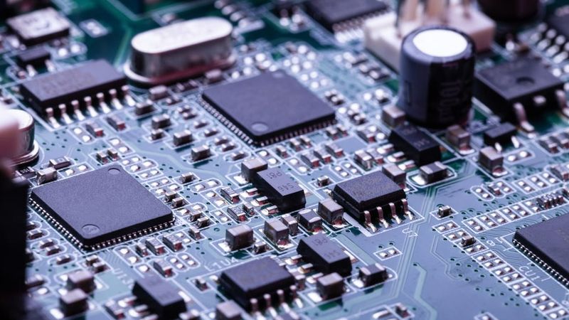
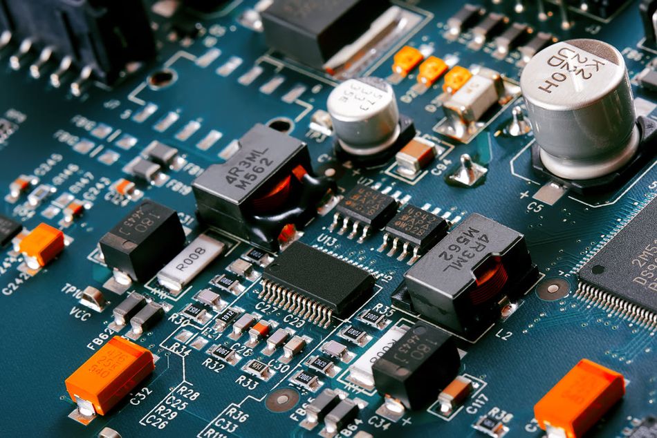
SMT PCB assembly mounts electronic components directly on the surface of printed circuit boards, allowing for high-density designs and miniaturization.
SMT has largely replaced through-hole assembly in modern manufacturing – over 90% of PCB assemblies use SMT due to its efficiency and cost advantages
An SMT assembly line typically includes automated solder paste printing, high-speed pick-and-place machines, and reflow ovens for soldering, followed by inspection (AOI/X-ray) to ensure quality.
Key equipment like stencil printers, pick-and-place machines, and reflow ovens work in tandem to precisely place thousands of components per hour, enabling the mass production of complex boards.
Industry standards (e.g., IPC-A-610 for assembly acceptability and IPC J-STD-001 for soldering) provide guidelines to ensure reliability, quality, and consistency in SMT PCB assembly.
Introduction
Almost every modern electronic device is built using SMT PCB assembly. It’s a process of mounting components directly onto the surface of circuit boards. It helps in the development of much smaller and more complex printed circuit board (PCB) designs compared to older through-hole methods. In fact, SMT has become the dominant assembly technology in the electronics industry, used in more than 90% of PCBAs today.
Why was SMT needed?
Before SMT, electronics were assembled with through-hole components inserted into drilled holes on the PCB. By the 1980s, as circuits became more complex, manufacturers needed a faster, more space-efficient method. Hence, Surface Mount Technology was introduced to cater to the needs for higher component density and automation.
Instead of wiring leads through holes, SMT solders flat leads or terminations of components onto copper pads on the board’s top surface. It’s a simple change that allows mounting of components on both sides of a board.
Eventually, it leads to smaller parts, and fully automated assembly, dramatically improving production speed and cost.
Suggested Reading: SMT Manufacturing: Everything You Need to Know
SMT vs. Through-Hole PCB Assembly
Through-Hole Technology THT has been a traditional mounting technique that has been used for decades in PCB design. When SMT broke through the industry, it slowly shoved away THT, providing a much different and efficient mounting option. So, let’s understand how Surface Mount Technology (SMT) differs from the traditional Through-Hole Technology (THT) assembly. Each approach has distinct methods and use cases:
Through-Hole Assembly (THT)
In Through-Hole Technology, the components have long leads or wires that are inserted into drilled holes in the PCB and soldered, usually on the opposite side.
It was a common method until the 1980s and is still used for connectors, large components, or high-stress applications.
Through-hole joints are mechanically strong
It’s a labor-intensive process and limits component density due to the required holes and lead spacing.

Surface Mount Assembly (SMT)
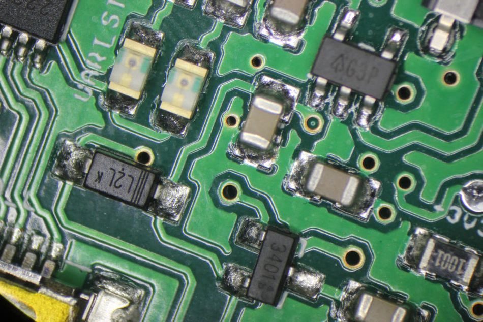
Components in SMT are also Surface Mount Devices (SMDs). They have flat contacts or short leads and are soldered onto pads on the board’s surface.
No drilling is needed for most parts
Components can be much smaller and placed on both sides of the PCB.
The process is almost entirely automated, which improves speed and consistency.
Key differences and advantages of SMT
Aspect | SMT Assembly (Surface Mount) | Through-Hole Assembly (THT) |
Component Mounting | SMD components are soldered on PCB surface pads. | Leads are inserted through drilled holes in the PCB. |
Component Size & Density | Very small packages (01005 chips ~0.4×0.2 mm) allow ultra-high density. Components can be mounted on both sides of the board. | Larger components and spacings; usually one side only. Leads to lower density due to hole and lead spacing limits. |
Assembly Speed & Automation | Placed by machines at thousands to tens of thousands of components per hour. Reflow ovens create many solder joints simultaneously. | Typically slower. Often hand-placed or wave soldered; less than 1000 placements/hour in manual or semi-auto processes |
Strength & Reliability | Excellent electrical performance; reliable in vibration. Slightly weaker mechanical attachment (solder only), so heavy or connector parts may need reinforcement. | Strong mechanical bonds (lead through hole). Better for parts that see mechanical stress (e.g. connectors). However, fewer parts can cause higher overall size/cost. |
Usage in Industry | Approx. 90% of modern PCB assemblies use SMT for efficiency and cost-effectiveness. Ideal for high-volume and complex boards. | Now used only where necessary (connectors, high-power parts, or legacy designs). Still important for some applications but much less common in new designs. |
As the table shows, SMT has clear advantages in size, speed, and automation, making it the default choice for most electronics. However, Through-hole still has niche uses (for example, rugged connectors or test points), and many boards use a mixed assembly of SMT and THT where appropriate.
Suggested Reading: Through Hole vs Surface Mount: Unveiling the Optimal PCB Assembly Technique
The SMT PCB Assembly Process and Equipment
SMT PCB assembly is a highly automated process with several stages. Each stage uses specialized equipment to place and solder components with precision. Below are the key steps in the SMT assembly process, from blank PCB to finished assembly:
Solder Paste Printing (Stencil Printing)
The first step is to apply solder paste to the PCB at all the component pad locations. This solder paste is a gray, putty-like mixture of microscopic solder alloy balls and flux. A stencil printer machine is used for this purpose.
A thin metal stencil (template) is aligned over the PCB, and a squeegee blade spreads paste across it, filling the stencil openings with paste on the pads below. Once the stencil is lifted, small deposits of paste remain on each pad.
This paste will later melt to form the solder joints. High-end stencil printers ensure even paste deposition and automatically clean excess paste for consistency.
Equipment Involved - Solder Paste Printer: This machine applies solder paste to PCB pads using a metal stencil. Most modern stencil printers have automated vision alignment to precisely register the stencil to the PCB, and they use pneumatic blades to wipe paste across. They often include paste deposition inspection and stencil cleaning systems to ensure consistent results for each board. A well-tuned printer can apply paste with an accuracy of a few microns in position and a controlled thickness on each pad.
Suggested Reading: Cutting-Edge Methods of Solder Paste Application for Electronics Manufacturing
Automated Component Placement
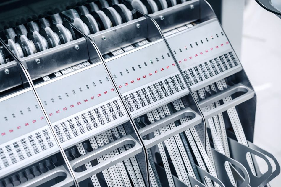
After the paste application, the PCB with wet solder paste deposits is transferred to the pick-and-place machine. It’s a robotic system that rapidly picks components from feeders and places them onto the PCB, exactly on the paste-coated pads.
The PCB components are supplied in tapes, reels, or trays and loaded into feeder slots. The machine’s head uses vacuum nozzles to pick up each component, uses vision cameras to orient and align it, and then lowers it onto the matching pads with solder paste.
Programming for pick-and-place uses the PCB’s design data to know the position of each component. Modern pick-and-place machines are extremely fast and precise. For instance, high-speed “chip shooter” models can place small components like resistors at tens of thousands of parts per hour, while slightly slower models handle larger or fine-pitch components with high accuracy.
So, an SMT line might use a fast chip shooter for tiny parts and a fine-placement machine for larger ICs, achieving both speed and precision. The result of this step is a PCB populated with all components held in place by the tackiness of the solder paste.
Equipment Involved
- Pick-and-Place Machine: The workhorse of SMT assembly, pick-and-place (PnP) machines accurately place SMD components onto the PCB. They consist of a moving head or multiple heads with vacuum nozzles, capable of picking components from tape reels, tubes, or trays. The machine uses high-speed cameras to center each component and correct for any mispick or rotation before placement. Its performance is measured in CPH (components per hour) and top level machines can exceed 50,000 CPH with a placement accuracy of around ±0.05 mm.
- Feeders: These are a critical part of PnP machines. Feeders present the components to the machine. Intelligent feeders can be quickly swapped and help with faster changeovers between jobs. In an SMT line, it’s common to have multiple PnP machines: e.g., one high-speed chip shooter for resistors/caps and another for larger ICs and odd-shaped parts, optimizing throughput.
Reflow Soldering
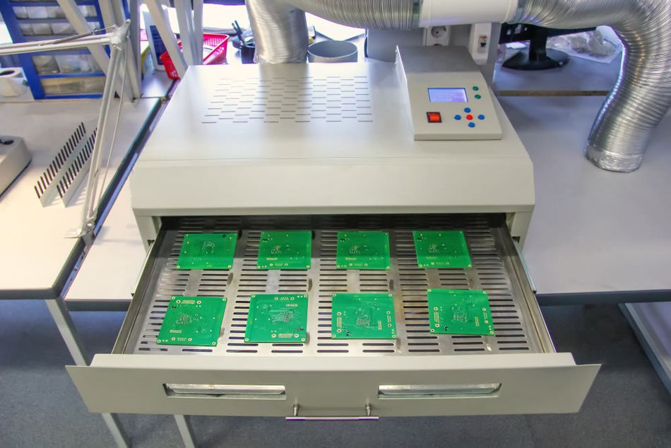
Once all components are placed on the PCB, the next step is to permanently solder them. This is done by carefully melting the solder paste in a reflow oven. The PCBAs are passed on a conveyor through a large reflow oven, which heats them in a controlled temperature profile.
A typical lead-free solder reflow profile has multiple zones:
Preheat region to gradually warm the board
Soak zone to activate flux and evenly heat all components
Peak reflow zone that reaches around 240–250 °C to melt the solder.
At the peak temperature, the solder particles in the paste melt and wet the component leads and pads, forming solder fillets. The board then enters a cooling zone where the solder solidifies, creating solid electrical and mechanical connections. Reflow ovens often have 8–10 heating zones and 1–2 cooling zones to shape this temperature profile precisely.
Modern ovens use forced convection for even heating and may include nitrogen atmosphere for quality. After reflow, the board emerges with all SMD components soldered in place. If the PCB has components on both sides, the SMT process can be repeated for the second side.
Suggested Reading: Solder Reflow: An In-Depth Guide to the Process and Techniques
Inspection and Quality Control
Reflow soldering is essentially the final step of assembly, after which the assembled boards undergo inspection. It is to ensure that all components are properly placed and soldered.
The most common method is AOI (Automated Optical Inspection), where high-speed cameras scan the PCB and compare the images to a reference to detect missing components, misalignments, insufficient solder, solder bridges, and other defects. AOI machines can detect many types of soldering issues quickly and are used immediately after reflow.
Moreover, specialized X-ray inspection (AXI) is used for hidden solder joints that optical systems can’t see. It checks for voids or shorts under the components. In addition to automated inspection, human visual inspection is often done for random samples or certain tricky areas as a double-check.
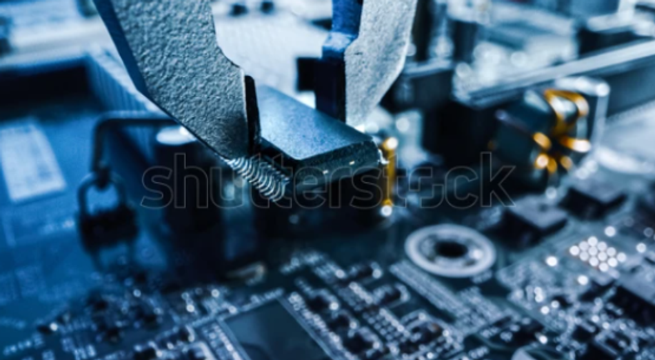
If any defects are found, the board may be sent for rework. It involves manually replacing or resoldering the problematic component using tools like hot-air rework stations or infrared heaters. For high-reliability products, some manufacturers also perform In-Circuit Testing or functional testing after assembly to verify that the circuit works as intended, catching any issues not visible by inspection.
Suggested Reading: PCB Inspection: Ensuring Quality and Reliability in Electronics Manufacturing
Other Tools and Equipment for SMT Assembly
A complete SMT line will also include board handling systems (automatic loaders, unloaders, and conveyors linking machines), reflow ovens as described, and sometimes conformal coating or selective soldering machines if the assembly requires those steps.
For boards that have through-hole components in addition to SMT, a wave soldering machine or selective soldering robot may be used after SMT reflow to solder the through-hole parts.
In rework departments, rework stations with hot-air guns, infrared heaters, microscopes, and soldering irons allow skilled technicians to fix any issues.
IC programming stations might also be present if programmable chips need their firmware loaded after assembly.
The combination of these advanced machines enables a high-throughput SMT assembly line to produce complex electronic boards with minimal human intervention. The initial programming and setup are crucial, but once set up, the line can assemble hundreds or thousands of boards with consistent quality.
Quality Standards and IPC Guidelines in SMT Assembly
Since SMT PCB assembly involves tiny scale components, consistency and adhering to quality standards is vital. Hence, organizations like Institute for Printed Circuits (IPC) developed a range of guiding standards for design, assembly, and inspection of PCB.
Some key standards relevant to SMT PCB assembly include:
IPC-A-610: “Acceptability of Electronic Assemblies”
IPC-A-610 provides visual criteria and guidelines for acceptable solder joint, component placement, and overall workmanship for assembled PCBs. It classifies assemblies into three classes (1, 2, 3) based on the required reliability.
Class 1 is for general electronics where occasional defects aren’t critical (e.g., consumer gadgets)
Class 2 is for dedicated service electronics requiring more reliability (most industrial and consumer products)
Class 3 is for high-reliability or life-critical electronics (e.g., aerospace, medical devices), which demand virtually zero defects and rigorous inspection.
Manufacturers will specify the class their product must meet, and IPC-A-610 gives the acceptance criteria (with many pictures) for inspectors to judge solder joints, component alignment, flux residue, etc.
Suggested Reading: IPC Class 2 vs Class 3: Understanding the Critical Differences in Electronics Manufacturing Standards
IPC J-STD-001: “Requirements for Soldered Electrical and Electronic Assemblies”
This standard is often used in conjunction with IPC-A-610. It focuses on the process and materials for soldering. J-STD-001 defines:
Soldering methods
Types of acceptable solders and fluxes
Process control like cleanliness and ESD
This standard sets acceptable criteria for solder joints from a process perspective. While IPC-A-610 is an inspection standard, J-STD-001 is a workmanship and process standard, including requirements like minimum solder fillet shapes, lead protrusion through holes, and even criteria for things like wire terminations. High-reliability industries often require compliance to J-STD-001 in their manufacturing.
IPC-7351: “PCB Land Pattern Design”
This standard provides guidelines for the design of pad layouts (land patterns) for surface mount components. It ensures that the PCB footprint for each component is optimized for soldering. For instance, too-small pads might lead to insufficient solder, while too-large pads could cause tombstoning of tiny parts, etc. PCB designers use this to properly dimension pads for various standard package sizes (like SOIC, QFP, BGA, 0402 resistor, etc.), taking into account the assembly process needs.
IPC-7711/7721: “Rework and Repair of Electronic Assemblies”
Even with high inspection and manufacturing standards, sometimes boards need rework. The IPC-7711/21 standard provides accepted methods to modify or repair assemblies without compromising reliability. This covers things like:
How to remove and replace components (including BGAs)
How to repair pads or traces if damaged
Criteria for an acceptable repaired board.
ESD and Handling Standards
While not IPC, standards like ANSI/ESD S20.20 define ESD control programs to protect sensitive components during assembly. Safe handling of boards (with ESD straps, ionizers, proper packaging) is part of quality assurance in SMT lines, preventing latent damage to ICs from static discharge.
In summary, quality standards like IPC provide the framework for excellence in SMT PCB assembly. By designing to standard guidelines and verifying assemblies against objective criteria, manufacturers can achieve high yield and reliability.
Suggested Reading: IPC Standards: The Definitive Guide for Electronics Engineers and PCB Designers
Conclusion
Surface Mount Technology (SMT) PCB assembly is a foundational process in modern electronics manufacturing. It promotes the large-scale production of densely populated and high-performance circuit boards. This assembly methodology comprises of a sequence of automated steps, starting with the solder paste application via stencil printing, followed by the precise placement of electronic components utilizing robotic pick-and-place machinery. Next, a controlled reflow soldering process establishes numerous electrical connections concurrently, culminating in a final inspection phase to identify and rectify any manufacturing anomalies.
Adapting to SMT assembly has significant advantages, such as improved manufacturing efficiency. Furthermore, SMT enables greater functional density within reduced physical dimensions. These benefits have established SMT as the predominant technique for PCB assembly, with through-hole technology now primarily reserved for specific component types, such as connectors and high-power devices. Consequently, a comprehensive understanding of SMT principles and practices is essential for professionals engaged in hardware design and electronics manufacturing.
FAQ
What is SMT PCB assembly?
SMT PCB assembly is the process of assembling electronic components onto a printed circuit board using Surface Mount Technology. Components are soldered directly on the board’s surface pads (instead of using drilled holes as in older through-hole methods). This involves applying solder paste, placing surface-mount components (SMDs) on the paste, and running the board through a reflow oven to solder everything. SMT PCB assembly enables very compact, high-density circuit boards since components can be small and placed on both sides of the PCB.
How does SMT differ from through-hole assembly?
In through-hole (THT) assembly, components have leads that go through holes in the PCB and are soldered on the opposite side, usually by hand or wave soldering. In SMT assembly, components are mounted on the surface with no need for holes (except for any mechanical support). SMT uses solder paste and reflow ovens, and is highly automated, whereas through-hole is slower and often manual. SMT allows much smaller component sizes and higher component density. However, through-hole joints are mechanically stronger, so they’re still used for connectors or large parts that endure mechanical stress. Many modern boards use mostly SMT parts and a few through-hole parts as needed (mixed assembly).
What are the main steps in the SMT PCB assembly process?
The key steps are:
Solder Paste Printing – applying solder paste to PCB pads using a stencil;
Pick-and-Place – using an automated machine to place SMD components onto the pasted pads;
Reflow Soldering – heating the assembly in a reflow oven to melt the paste and solder the components;
Inspection – checking the assembled board for any placement or soldering defects (using AOI, X-ray, etc.).
What equipment is used in SMT PCB assembly?
A typical SMT assembly line uses several specialized machines. The primary ones are: a Stencil Printer (for solder paste application), a Pick-and-Place Machine (to automatically place components), and a Reflow Oven (to solder the components by melting the paste). In addition, there are often SPI (Solder Paste Inspection) systems to check paste deposition and AOI (Automated Optical Inspection) machines to inspect finished boards. Other auxiliary equipment includes PCB loaders/unloaders, conveyors, and rework stations for fixing any issues. Together, this equipment allows fast and precise assembly of PCBs with minimal human intervention.
What industry standards ensure quality in SMT assembly?
The electronics industry relies on standards from organizations like IPC to maintain quality. For SMT assembly, IPC-A-610 is the key standard outlining the acceptable workmanship (solder joint criteria, component alignment, etc.) for assembled boards. IPC J-STD-001 defines requirements for the soldering process and materials. These standards classify products by quality levels (Class 1/2/3) depending on reliability needs. Other relevant standards include IPC-7351 (guidelines for PCB pad design for surface mount components) and IPC-7711/7721 (procedures for reworking and repairing boards). While not legally required, following these standards is considered best practice and is often required by customers in high-reliability sectors.
Can a PCB have both SMT and through-hole components?
Yes, many PCBs use a mixed assembly approach. SMT components are used for the majority of parts (resistors, ICs, capacitors, etc.), and through-hole components are used for parts that benefit from the mechanical strength of leaded attachment or are not available in SMT packages. Examples include connectors, large electrolytic capacitors, or unique modules. In manufacturing, the SMT parts are assembled and reflow soldered first. Then, the through-hole parts are typically soldered afterward, either manually or using a wave soldering process (or selective soldering for specific spots). Mixed technology boards are common – they leverage the advantages of SMT for most of the circuitry while still accommodating a few through-hole parts as needed.