555 Timer Circuit: Theory and Practice for Modern Engineers
This article explores the theoretical foundations of the 555 timer circuit — covering architecture, modes of operation, timing calculations, design considerations and cutting-edge applications.

16 Dec, 2025. 15 minutes read
555 Timer Circuit
Key Takeaways
The 555 timer is a classic integrated circuit used for timing, oscillation and pulse generation, consisting of comparators, a flip‑flop and transistor/resistor networks.
It operates in three primary modes — astable, monostable, and bistable — each defined by simple RC networks that yield predictable pulse widths and frequencies.
The practical applications span LED flashers, PWM generators, audio oscillators, motion detectors and more; modern low‑power variants extend their utility into battery‑powered and eco‑friendly designs.
Simple formulas relate timing intervals to resistor and capacitor values; selecting appropriate components is critical for accuracy and stability.
While newer timing ICs offer lower power consumption and broader voltage ranges, the 555 timer circuits remain valuable for educational purposes and quick prototyping.
Introduction
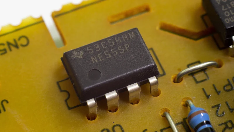
Since its debut in 1972, the 555 timer circuit has become one of the most popular components in electronics, valued for its simplicity, reliability, and versatility. Since its introduction, it has remained a foundational component for generating precise time delays, oscillations, and pulse-width modulation signals in both analog and mixed-signal systems. This device integrates comparators, a flip-flop, a voltage divider, and a discharge transistor, enabling flexible operation in monostable, astable, and bistable modes. More than one billion units are produced annually, attesting to its widespread adoption.
In modern engineering applications, the 555 timer circuit continues to play a practical role in prototyping, educational environments, and cost-sensitive designs where simplicity is critical. This article explores the theoretical foundations of the 555 timer circuit — covering architecture, modes of operation, timing calculations, design considerations and cutting-edge applications.
Background and Historical Context
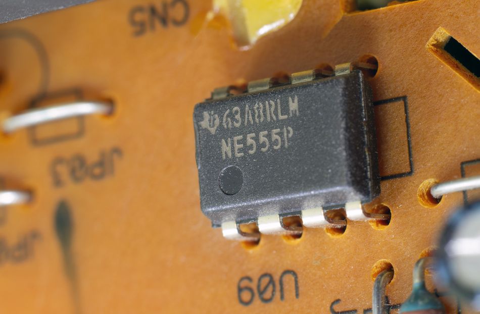
The 555 timer was designed in 1971 by Hans Camenzind while working at Signetics to create a low-cost, highly reliable universal timing device. [1] Its oscillation frequency was meant to remain stable despite temperature changes and supply-voltage variations. The result was the NE555, a bipolar integrated circuit that rapidly became a cornerstone of analog and mixed-signal electronics. Internally, the original device consisted of approximately 25 bipolar transistors, 15 resistors, and 2 diodes fabricated on a single silicon die and housed in an 8-pin dual-in-line package (DIP).
The internal architecture of the 555 timer — based on voltage comparators, a flip-flop, and a discharge transistor — enabled precise timing and oscillation using only a few external components. Its popularity was further reinforced by its wide operating supply voltage range of 5 V to 18 V and its ability to source or sink up to 200 mA of output current, making it suitable for directly driving relays, LEDs, and small motors. Over time, derivative devices such as the dual 556 and quad 558/559 timers were introduced to support multi-channel timing applications.
Modern CMOS implementations, including the 7555 and LMC555, retain the original functional architecture. [2] They offer significantly reduced power consumption, improved input impedance, and enhanced suitability for battery powered and low-voltage designs. Despite advances in digital timing solutions, the 555 timer remains relevant, with its fundamental design essentially intact for more than five decades.
Recommended Reading: Concurrent-Mode CMOS Detector IC for Sub-Terahertz Imaging System
Internal Architecture and Operating Principles
Block Diagram Overview
The 555 timer integrated circuit is a carefully balanced analog control system built around two voltage comparators, an RS flip-flop, a discharge transistor, and a precision resistive voltage divider composed of three internal 5 kΩ resistors. This divider establishes two stable reference voltages at one-third and two-thirds of the supply voltage (VCC), which serve as the primary timing control thresholds.
The comparators continuously monitor the voltage present at the threshold input and trigger input, both of which are typically connected to an external timing capacitor. Once the capacitor voltage crosses either reference level, the corresponding comparator changes state and drives the flip-flop. The output of the flip-flop directly controls both the output stage and the discharge transistor, coordinating the charge and discharge cycles of the capacitor. This interaction enables highly predictable timing behavior that is largely independent of component tolerances and supply voltage fluctuations.
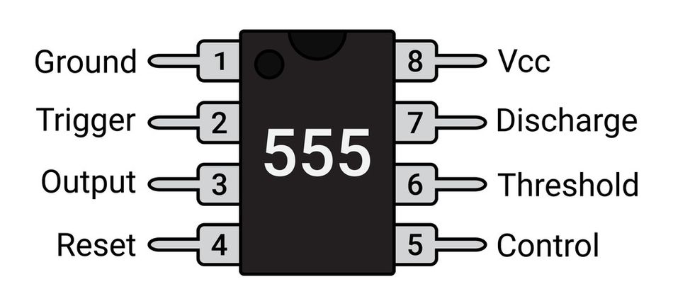
Pin Functions
Understanding each pin is essential for configuring the timer:
Pin | Name | Description |
1 | Ground | Reference ground for circuit operation |
2 | Trigger | Input that sets the flip‑flop when the voltage drops below 1/3 Vcc |
3 | Output | Push‑pull output that sources or sinks current up to ~200 mA |
4 | Reset | Active‑low input that forces the output low when pulled low |
5 | Control Voltage | Allows external modulation of the threshold; typically bypassed for noise immunity |
6 | Threshold | Resets the flip‑flop when the voltage exceeds 2/3 Vcc |
7 | Discharge | Open‑collector output is used to discharge the external capacitor |
8 | Vcc | Supply voltage (5–18 V for bipolar devices, 2–15 V for CMOS variants) |
Comparator and Flip‑Flop Operation
The operating principle of the 555 timer relies on a simple analog logic. Once the trigger input voltage drops below 2/3rd of VCC, the lower comparator sets the RS flip-flop. This action drives the output pin high and turns off the discharge transistor, allowing the timing capacitor to charge through external resistors. [3]
Once the capacitor voltage rises and exceeds 2/3rd of VCC, the upper comparator resets the flip-flop. The output is driven low, and the discharge transistor is switched on, providing a low-impedance path to ground that rapidly discharges the capacitor. This repetitive comparison-and-switching mechanism forms the fundamental basis of all monostable, astable, and bistable operating modes of the 555 timer.
Recommended Reading: X5R vs X7R: Comprehensive Comparison & Engineering Design Guide 2025
Modes of Operation
The 555 timer can be configured in several modes by connecting external resistors and capacitors. The three primary modes are described as:
Astable Mode (Free‑Running Oscillator)
In astable mode, the 555 operates as an oscillator that continuously produces a square wave output. The timing capacitor repeatedly charges and discharges between 1/3 VCC and 2/3 VCC, controlled by two external resistors (R₁ and R₂) and the internal discharge transistor. [4] This configuration enables reliable pulse generation with predictable frequency and duty cycle.
The timing equations are:
High Time: tₕ = ln(2) × (R₁ + R₂) × C
Low Time: tₗ = ln(2) × R₂ × C
Frequency: f = 1 / [ln(2) × (R₁ + 2R₂) × C]
With these formulas, designers can compute resistor and capacitor values to achieve a specific frequency. For example, to generate ~1 kHz using standard values, one might choose R₁ = 8.2 kΩ, R₂ = 68 kΩ and C = 10 nF.
Design Considerations
Duty Cycle: Because charging occurs through R₁ + R₂ while discharging occurs only through R₂, the duty cycle is inherently greater than 50%. Adding a diode in parallel with R₂ allows independent control of charge and discharge paths, enabling near-symmetric waveforms.
Frequency Range: Bipolar 555 devices typically operate reliably up to 100–500 kHz, while CMOS variants can reach several megahertz.
Temperature Stability: Resistive and capacitive components influence frequency stability. Use precision components and consider temperature coefficients.
Typical Applications
Clock Generation: Used as a low-cost clock source for counters, shift registers, and microcontroller timing tests where high precision is not critical.
LED Flashers and Indicators: Common in status indicators, warning flashers, and visual alarms. Adjusting the timing capacitor or resistor value directly controls the blink rate.
PWM and Motor Speed Control: With diode steering or a potentiometer, the duty cycle can be adjusted to generate PWM signals for DC motor speed control, lamp dimming, or heater regulation.
Audio Tone Generation: Square-wave audio tones for buzzers, alarms, and test signal injection in audio amplifiers.
Signal Testing and Debugging: Provides a quick test waveform during prototyping on a breadboard without requiring a microcontroller.
Monostable Mode (One‑Shot Timer)
In monostable mode, the 555 produces a single output pulse of a fixed duration in response to a trigger. The resistor (R) and a capacitor (C) connected to the discharge pin set the pulse width. When the trigger input momentarily goes low, the flip‑flop sets, turning the output high and allowing the capacitor to charge through R. Once the capacitor voltage reaches 2/3 Vcc, the output resets and the capacitor discharges through the discharge transistor.
In monostable mode, the 555 functions as a one-shot pulse generator with a single stable state. An external resistor (R) and capacitor (C) connected to the discharge pin define the output pulse width. When the trigger pin is momentarily driven low, the flip-flop sets, the output goes high, and the capacitor begins charging through R. Once the capacitor voltage reaches 2/3 VCC, the output returns low, and the capacitor rapidly discharges.
The pulse width (time high) is given by:
tₚ = ln(3) × R × C ≈ 1.1 × R × C
For example, R = 100 kΩ and C = 10 µF yield a pulse duration of approximately 1.1 seconds. By varying RC values, pulse widths can range from microseconds to several hours.
Typical Applications
Time Delay Circuits: Creating startup delays in power-up sequences, relay activation delays, or watchdog recovery timing.
Switch Debouncing: Converting noisy pushbutton or mechanical switch inputs into clean, single transitions.
Event Timing and Measurement: Measuring intervals between events or generating precisely timed enable signals.
Pulse Stretching: Expanding narrow trigger pulses into longer logic-level pulses suitable for digital processing.
Security and Alarm Systems: Generating controlled activation periods for sirens, lights, or control relays.
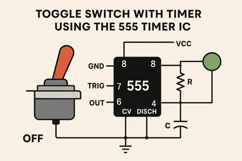
Bistable Mode (Flip‑Flop)
In bistable mode, the 555 operates as a simple RS latch, with no timing capacitor required. The trigger input acts as the set control, while the threshold input functions as a reset. Pulling the trigger low forces the output high; pulling the threshold low forces the output low. The output remains latched until an opposing input event occurs.
Typical Applications
Toggle Switches: Implementing push-button controlled ON/OFF logic without microcontrollers.
Simple Memory Elements: Storing binary state information in small control systems.
Power Control Latches: Soft-power switches that control MOSFET-based power stages.
User Interface Logic: Mode selection or enable/disable control in embedded systems.
Schmitt Trigger Operation
The 555 can operate as a Schmitt trigger inverter by connecting the trigger and threshold pins together and applying the input signal to both. This configuration provides hysteresis and converts noisy signals into clean logic transitions.
Typical Applications
Sensor Signal Conditioning: Cleaning noisy signals from temperature sensors, light sensors, or mechanical encoders.
Waveform Shaping: Converting sine or ramp waveforms into square waves for digital logic.
Noise Immunity Improvement: Preventing false triggering in electrically noisy environments.
Level Detection: Acting as a comparator with hysteresis for threshold-based control systems.
Recommended Reading: Types of Switches: Complete Engineering Guide for 2025
Practical Implementation: Schematic, Breadboard Setup, and Measured Waveforms
Implementing a 555 timer circuit in hardware requires careful attention to component selection, wiring practices, and power integrity to ensure predictable operation.

While the internal architecture of the IC is robust, external layout and component quality directly influence timing accuracy, noise immunity, and output stability.
Schematic-Level Considerations
The designer selects the timing resistor, timing capacitor, and operating mode configuration based on the desired timing interval, pulse width, or duty cycle at the schematic stage. The datasheet provided by the manufacturer specifies absolute maximum ratings, recommended supply voltage (VCC) ranges, and output current limits that must be observed.
The control voltage pin should typically be bypassed to GND using a small capacitor (≈10 nF) to improve noise immunity. The reset pin must be tied to VCC if unused to prevent unintended resets caused by noise or voltage drop. Proper decoupling of the power supply with ceramic capacitors close to the IC is essential, especially in high-frequency or PWM applications.
Breadboard and Prototyping Practices
When assembling a 555 timer module on a breadboard, short connections and a clear ground reference reduce parasitic capacitance and unwanted coupling. Electrolytic capacitors used for long delays must be oriented correctly, and resistor values should be verified to avoid large timing errors. For adjustable designs, a potentiometer allows fine control of frequency or pulse duration during testing.
Output Behavior and Waveforms
The output stage delivers a strong digital signal, switching cleanly between output high and output low levels. On an oscilloscope, the timer output appears as a square wave in astable mode or a single pulse in monostable operation. Observing the voltage across the timing capacitor reveals the characteristic exponential charge and discharge waveforms between the internal reference thresholds.
Recommended Reading: Potentiometer Schematic: Theory, Types, and Practical Implementations for Engineers
Practical Implementations and Projects
The versatility of the 555 timer circuit is best demonstrated through practical implementations. From simple educational projects to sensor interfacing and industrial control, the device enables a wide range of real-world applications using minimal external components.
Let’s go through some of the notable ones below:
1. LED Flasher (Astable Mode)
One of the simplest 555 projects is an LED flasher, often used in electronics courses. Configure the timer in astable mode; the output toggles between high and low, driving the LED on and off. By selecting R1, R2 and C values, you can set the blink rate.
For example, R₁ = 1 kΩ, R₂ = 10 kΩ and C = 100 µF yield a period of approximately 0.76 s.
The applications include status indicators, warning lights, fault alerts, and beginner-level timing experiments.
2. Monostable Delay Timer
In monostable mode, the 555 functions as a one-shot timer, generating a single output pulse of fixed duration when triggered. The pulse width depends on a single resistor-capacitor network connected to the threshold pin and discharge pin.
Using R = 220 kΩ and C = 47 µF yields a pulse duration of approximately 11.3 seconds. This configuration is ideal for applications where a controlled time delay is required after a trigger event.
The applications include relay hold timers, appliance control, camera shutter delays, staircase lighting, and power-on reset circuits.
3. PWM Generator
By operating the 555 in astable mode and modulating the control voltage pin, the circuit can function as a PWM generator. A potentiometer allows continuous adjustment of the duty cycle while keeping the frequency nearly constant. This technique avoids changing resistor values and improves control resolution. PWM generation using the 555 is commonly paired with a MOSFET at the output stage to control higher loads.
The applications include DC motor speed control, LED brightness control, heater regulation, and power control modules.
4. Tone Generator
Once configured for audio frequencies, the 555 timer acts as a simple tone generator. By selecting appropriate R₁, R₂, and C values, the oscillation frequency can be placed in the audible range (approximately 400 Hz to 2 kHz). The output pin drives an external amplifier or transistor to power a speaker.
The applications include buzzers, alarms, test tone sources, and audio signal injection.
5. Motion Detector and Sound‑Operated Timer
The 555 timer is frequently combined with external sensors to create event-driven systems. In a motion detector, a PIR sensor triggers a monostable circuit, causing the output to remain high for a preset duration after motion is detected. Similarly, a sound-operated timer uses a microphone and amplifier stage to trigger the trigger input.
The applications include intrusion alarms, automatic lighting, occupancy detection, and home automation triggers.
6. PWM Audio Amplifier
The 555 timer operating in astable mode can generate a PWM signal at high frequency (65–188 kHz), which is then filtered and amplified to drive speakers. This signal is amplified to drive speakers, demonstrating a basic Class-D–style amplifier concept, after filteration. Despite not being suitable for high-fidelity audio, it provides valuable insight into PWM-based amplification.
The applications include educational audio experiments, low-power audio systems, and signal processing demonstrations.
7. Soil Moisture Meter
Recent designs demonstrate the use of a 555 timer circuit in sensor instrumentation. In a soil moisture meter, the resistance between probes varies with moisture content. This resistance influences the pulse width of a monostable output, allowing moisture levels to be inferred digitally. [5]
The applications include agricultural monitoring, irrigation control, environmental sensing, and IoT preprocessing stages.
8. Build‑Your‑Own 555 Timer
For educational purposes, some enthusiasts build a discrete transistor version of the 555 to understand its inner workings. Constructing a discrete version of the 555 using individual transistors, resistors, and diodes provides deep insight into its internal operation. This project illustrates how the comparators, flip-flop, and output stage interact to create stable timing behavior.
The applications include electronics education, analog circuit training, and semiconductor fundamentals.
9. Industrial On‑Off Timer with RF Remote
More advanced designs use multiple 555 timers to implement independent ON and OFF timing intervals. When combined with an RF remote or logic interface, these timers can control industrial loads at scheduled intervals without microcontrollers.
The applications include motor duty cycling, pump controllers, industrial automation, and scheduled equipment operation.
10. Astable Multivibrator for Sequential Lights
In this project, a 555 operating as an astable multivibrator provides clock pulses to counters or logic circuits that sequentially activate LEDs. This approach forms the foundation of chasing lights and pattern generators.
The applications include decorative lighting, signage, display systems, and educational logic experiments.
Recommended Reading: What Is a PWM Signal? Fundamentals and Practical Applications for Engineers
Design Calculations and Tables
To design a stable 555 timer circuit, it helps to standardize around the core timing equations and then use tables as quick starting points.
Astable Mode Example Values
These rows assume R₁ = 8.2 kΩ and R₂ = 68 kΩ (chosen to keep current reasonable and duty cycle near ~53%). Frequency is set mainly by scaling the timing capacitor.
Desired Frequency | Capacitance (C) | R₁ (kΩ) | R₂ (kΩ) | Duty Cycle | Period |
0.1 Hz | 100 µF | 8.2 | 68 | 52.8% | 10.0 s |
1 Hz | 10 µF | 8.2 | 68 | 52.8% | 1.0 s |
10 Hz | 1 µF | 8.2 | 68 | 52.8% | 100 ms |
100 Hz | 100 nF | 8.2 | 68 | 52.8% | 10.0 ms |
1 kHz | 10 nF | 8.2 | 68 | 52.8% | 1.0ms |
10 kHz | 1 nF | 8.2 | 68 | 52.8% | 100 µs |
100 kHz | 100 pF | 8.2 | 68 | 52.8% | 10.0 µs |
Why This Works? Reducing capacitance by 10× increases frequency by ~10×, while duty cycle stays nearly constant because it depends mainly on the resistor ratio.
Monostable Mode Example Values
These values assume R = 91 kΩ and scale C to set the pulse width:
Pulse Duration | Capacitance (C) | Resistance (R) |
100 µs | 1 nF | 91 kΩ |
1 ms | 10 nF | 91 kΩ |
10 ms | 100 nF | 91 kΩ |
These values serve as starting points. Adjust R or C proportionally to achieve the desired pulse lengths.
Modern Developments and Alternatives
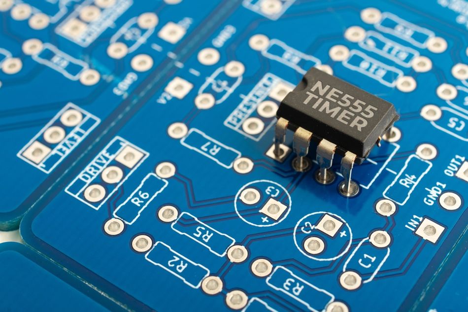
While the 555 timer remains a reliable workhorse, engineers should be aware of advancements in timer ICs. Devices such as the LM556 (dual timer), ICM7555 and LMC555 (CMOS variants), and specialized ICs like the LTC6991 voltage-controlled oscillator offer improved performance in many contemporary applications. These newer devices typically feature lower quiescent current, extended supply voltage flexibility, and improved stability, making them well-suited for battery-powered and energy-efficient designs.
The 555 timer IC continues to be favored for rapid prototyping, educational use, and cost-sensitive commercial products. Its forgiving design tolerates component variations, electrical noise, and layout imperfections better than many precision devices. Availability in both DIP and surface-mount packages further ensures its continued use in laboratory and production environments.
Nevertheless, the 555 remains relevant for quick prototypes, educational demonstrations and simple commercial products. Its availability in DIP and SMD packages and its forgiving design tolerate noise and component tolerances. Once selecting a timer, consider the following:
Power Consumption: For battery‑powered applications, a CMOS 555 variant or a modern low‑power timer may be preferable.
Voltage Range: Choose a timer that matches your supply voltage. Some CMOS versions work down to 2 V.
Precision: If timing accuracy is critical, use precision capacitors and resistors or choose a microcontroller with built‑in timers.
Complexity: For complex waveforms or digital integration, microcontrollers or dedicated PWM chips may offer more flexibility.
Recommended Reading: IC Package Types: A Comprehensive Guide
Design Best Practices
Reliable operation of a 555 timer circuit depends as much on implementation as on theoretical design. The following best practices improve stability, repeatability, and robustness.
Decoupling Capacitors: Place a 0.1 µF ceramic capacitor close to the IC’s Vcc and ground pins to reduce noise and ensure stable operation. Additional electrolytic capacitors (1–10 µF) may help when driving heavy loads.
Control Voltage Filtering: Pin 5 (control voltage) should be bypassed with a small capacitor (typically 10 nF) to ground to prevent threshold noise and improve stability.
Component Tolerances: Timing accuracy depends on resistor and capacitor tolerances. Use 1% metal film resistors and film capacitors for precision. Electrolytic capacitors have high tolerances (±20%) and vary with temperature and voltage.
Temperature Compensation: The 555’s internal threshold is proportional to Vcc; variations in supply voltage affect timing. Use regulated power supplies or include voltage reference circuits for stability.
Output Loading: The 555 can source or sink up to 200 mA, but driving inductive loads (relays or motors) requires flyback diodes or driver transistors to protect the IC.
Reset Pin: Tie pin 4 to Vcc if unused to prevent accidental resets. For external control, apply a logic signal to reset the timer asynchronously.
Testing and Simulation: Before building, simulate the circuit in SPICE or use 555 calculators to verify timing and waveform integrity.
Common Failure Modes and Troubleshooting Checklist
Despite its simplicity, the 555 timer circuit can exhibit unreliable behavior if the design, wiring, or component choices are incorrect. Understanding common failure modes helps engineers quickly diagnose issues during prototyping and deployment.
Common Failure Modes
No Output or Stuck Output (Always High or Low)
This typically results from an incorrectly wired reset pin, which must be tied to VCC if unused. A missing or unstable power supply connection, incorrect GND reference, or a damaged IC can also force the output into a fixed state.
Incorrect Timing Interval
Timing errors usually stem from incorrect resistor values, capacitor tolerance issues, or polarity errors in electrolytic capacitors. Leakage current in large-value capacitors can significantly alter the amount of time generated, especially in long-delay monostable circuits.
Unstable or Jittery Output
Noise on the control voltage or supply voltage can cause the comparators to toggle unpredictably. Insufficient decoupling or long breadboard wires often introduce interference, leading to distorted waveforms or irregular pulse widths.
False Triggering
Noisy inputs on the trigger pin, commonly from a mechanical pushbutton, can cause unintended retriggering. Without proper debouncing, the flip-flop may toggle multiple times from a single event.
Output Cannot Drive Load
Although the output stage can source or sink significant output current, heavy or inductive loads may cause voltage drop, overheating, or IC failure if not isolated with a MOSFET, transistor, or flyback diode.
High Power Consumption
Using a bipolar 555 in battery-powered systems may result in excessive current draw. CMOS variants are preferred when low-power operation is required.
Troubleshooting Checklist
Verify VCC and GND connections and confirm the supply voltage is within datasheet limits
Tie the reset pin to VCC if not externally controlled
Measure the timing capacitor voltage; it should ramp cleanly between 1/3 and 2/3 VCC
Check resistor and capacitor values with a multimeter before installation
Add a 0.1 µF decoupling capacitor close to the IC supply pins
Bypass the control voltage pin with a 10 nF capacitor to reduce noise
Use proper pull-up resistors or debouncing networks on trigger inputs
Isolate high-current or inductive loads using external drivers
Observe the timer output and capacitor waveforms with an oscilloscope
Replace the IC if all external components verify correctly
Debugging Tip
Upon diagnosing issues, temporarily reduce component values to shorten timing intervals. Faster cycles make errors easier to observe and confirm before scaling to longer delays.
Recommended Reading: Clock Gating: Powering Down Idle Circuits
Conclusion
The 555 timer circuit remains a cornerstone of electronic design, combining simplicity, versatility and low cost. Its internal architecture of comparators, a flip‑flop and RC networks allows it to function as an oscillator, one‑shot timer, latch or Schmitt trigger. By selecting appropriate resistors and capacitors, engineers can design circuits that generate precise delays or oscillations across a wide frequency range. The ability of the 555 timer to source and sink moderate currents makes it suitable for driving LEDs, relays and small speakers. Modern improvements have produced low‑power CMOS versions and alternative timing ICs with greater efficiency and precision. Yet the classic 555 continues to serve as a valuable teaching tool and prototyping solution. With careful component selection, decoupling and design considerations, it can deliver reliable performance even in demanding applications.
Frequently Asked Questions
1. What supply voltage does the 555 timer require?
A. Bipolar 555 timers operate from 5–18 V, while CMOS variants function reliably down to approximately 2 V.
2. What is the typical output current capability of a 555 timer?
A. The output stage can source or sink up to 200 mA, sufficient for LEDs, relays, or transistor drivers.
3. What determines the frequency of a 555 timer in astable mode?
A. The oscillation frequency is set by two resistors and one timing capacitor connected to the threshold and discharge pins.
4. Why use a capacitor on pin 5 (control voltage)?
A. A small capacitor (≈10 nF) connected from pin 5 to ground filters noise and stabilizes the internal voltage divider, improving timing accuracy.
5. What is the maximum frequency a 555 timer can generate?
A. Bipolar versions typically reach 100–500 kHz, while CMOS implementations can exceed 2 MHz depending on design and layout.
6. How many transistors, diodes and resistors are inside a standard 555?
A. The classic bipolar 555 contains approximately 25 transistors, 15 resistors, and 2 diodes on a single silicon die.
7. What are some alternative timer ICs?
A. Options include the dual 556, quad 558/559, and modern low‑power devices like the ICM7555. Evaluate them based on power consumption, voltage range and features.
References
[1] Digilent. 555 Timer IC: History, Basics & Working Principle [Cited 2025 December 13] Available at: Link
[2] Texas Instruments. LMC555 CMOS Timer datasheet (Rev. N) [Cited 2025 December 13] Available at: Link
[3] PSU. The 555 Timer IC - Details and Operation [Cited 2025 December 13] Available at: Link
[4] HIBP. 555 Timer [Cited 2025 December 13] Available at: Link
[5] ARPN Journals. A Digital Soil Moisture Meter using the 555 Timer [Cited 2025 December 13] Available at: Link
in this article
1. Key Takeaways2. Introduction3. Background and Historical Context4. Internal Architecture and Operating Principles5. Modes of Operation6. Practical Implementation: Schematic, Breadboard Setup, and Measured Waveforms7. Practical Implementations and Projects8. Design Calculations and Tables9. Modern Developments and Alternatives10. Design Best Practices11. Common Failure Modes and Troubleshooting Checklist12. Conclusion13. Frequently Asked Questions14. References