MOSFET Symbol: Theory, Practical Usage and Future Trends
Learn everything about the MOSFET symbol, from what its shapes and arrows mean to how it is used in digital design and power electronics. This article covers NMOS/PMOS symbols, modes, intrinsic body diodes, selection criteria, modern FinFET, wide bandgap devices, and the latest market trends.

22 Oct, 2025. 16 minutes read

MOSFET - Structure
Introduction
Metal‑oxide‑semiconductor field‑effect transistors (MOSFETs) are the workhorses of modern electronics. They power digital logic gates, microprocessors, power converters, motor drives, and radio‑frequency circuits. The MOSFET symbol encapsulates the functional identity of one of the most versatile components in electronics. For circuit designers and students, reading a MOSFET symbol correctly is fundamental: the symbol tells you whether the device is an n‑channel or p‑channel transistor, whether it is normally off or normally on, and how its intrinsic diode is oriented.
In modern power electronics, the MOSFET symbol also guides design decisions related to gate driving, protection, and switching efficiency. This article explores the theoretical basis, practical implications, and future trends of MOSFET symbols to help engineers strengthen both their analytical and design capabilities in contemporary and next-generation electronic systems.
Anatomy of the MOSFET symbol
Basic Terminals and Layout
The discrete metal-oxide-semiconductor field effect transistor (MOSFET) is built around four essential terminals — the gate (G), drain (D), source (S), and body or substrate (B). In most practical packages, the body is internally connected to the source terminal, leaving only three pins accessible to circuit designers. This simplifies circuit integration and minimizes unwanted parasitic conduction paths.
The MOSFET symbol graphically conveys this structure: the vertical line represents the channel between the drain and source, while the horizontal line denotes the gate terminal, separated by a small gap symbolizing the oxide layer — the insulating barrier responsible for the high input impedance of MOSFET. The presence or absence of a body connection in the schematic often indicates whether the device is discrete or integrated.
Historically, the earliest MOSFET symbols evolved from JFET notations used in the 1950s, where the curved gate physically touched the channel. When engineers began adopting the insulated gate concept of MOS technology in the early 1960s, the gap between the gate and channel was introduced to visually depict the oxide insulation. Over time, the standardized MOSFET symbols used today became essential to distinguish between n-channel and p-channel devices, particularly in integrated circuits and CMOS logic gates.
The broken channel line signifies an enhancement-mode MOSFET, indicating the device is normally off until a sufficient gate-source voltage (VGS) is applied. Conversely, a solid channel line represents a depletion-mode MOSFET, meaning the channel conducts at zero gate bias and requires reverse polarity on the gate terminal to switch off.
Arrow Orientation and Polarity
The arrow within the MOSFET symbol is one of the most critical visual indicators of device polarity. It always points from the P-type region to the N-type region — a convention derived from the direction of hole current flow.
For an n-channel MOSFET (NMOS), the channel is N-type, and the body (substrate) is P-type, causing the arrow to point into the channel. The helpful mnemonic engineers use is “n is in.” In contrast, a p-channel MOSFET (PMOS) has an N-type body and a P-type channel, so its arrow points outward. [1]
In three-terminal symbols (where the body is tied to the source), the arrow originates from the source terminal and points toward (for NMOS) or away from (for PMOS) the channel. In four-terminal MOSFET symbols, the arrow is drawn directly on the body lead. This small but powerful visual cue helps engineers instantly recognize the type of MOSFET and its biasing polarity in any schematic diagram.
Enhancement Mode vs. Depletion Mode
MOSFETs operate primarily in two distinct conduction modes — enhancement mode and depletion mode, each with unique characteristics and design implications.
Enhancement-Mode MOSFETs (Normally Off): These are the most common in digital circuits and power electronics. No drain current (ID) flows when VGS = 0, and the device turns on only when the gate-source voltage (VGS) exceeds a specific threshold voltage (Vth). For n-channel MOSFETs, conduction begins when VGS > Vth, while p-channel MOSFETs require a sufficiently negative voltage to turn on. The MOSFET symbol for enhancement mode shows a broken or dashed channel line, visually emphasizing that conduction does not exist at zero bias.
Depletion-Mode MOSFETs (Normally On): In contrast, depletion-mode MOSFETs conduct at zero gate bias because a channel already exists. Applying a reverse gate voltage depletes the charge carriers (electrons or holes) and reduces the drain current. These devices are symbolized with a solid channel line. While less common in digital logic, they are invaluable in analog amplifiers, voltage regulators, and specialized current sources, where a normally-on characteristic is desirable.
Historically, depletion MOSFETs were favored in early analog computers and JFET replacement circuits before enhancement-mode MOSFETs dominated CMOS and power supply design.
Intrinsic Body Diode and Parasitic Effects
Every real MOSFET contains internal parasitic components that influence its behavior. The p-n junction formed between the body and drain acts as an intrinsic body diode, also known as a parasitic diode. This diode conducts when the drain-source voltage (VDS) becomes reverse-biased, allowing current flow in the opposite direction.

In a power MOSFET, this body diode is often illustrated explicitly in the MOSFET symbol, showing its orientation — from body to drain in NMOS, and from drain to body in PMOS. Designers must account for this diode when dealing with inductive loads, using it for freewheeling currents, or supplementing it with external Schottky diodes for better efficiency and switching performance.
However, the body-drain-substrate junction can also introduce unwanted bipolar transistor (BJT) behavior, leading to latch-up in integrated CMOS circuits. To prevent this, the p-type substrate of NMOS transistors is connected to ground, and the n-type substrate of PMOS transistors is tied to the voltage at the drain (VDD), ensuring stable biasing and isolation.
Variations and Alternative Notations
Different MOSFET symbols exist to meet diverse engineering disciplines and schematic standards:
Body-Dot Notation: Instead of using arrows, a small dot on the gate terminal denotes a PMOS device, while the absence of a dot signifies NMOS. This compact form is frequently used in IC schematics and logic design diagrams.
Compact CMOS Representation: In CMOS logic gates, the n-channel transistor is drawn with a solid line (representing the channel), while the p-channel transistor uses a broken line. Arrows are often omitted because body connections are implicit. These symbols simplify pull-up and pull-down network design in digital ICs.
JFET and IGFET Symbols: A JFET (Junction Field Effect Transistor) uses a curved gate line that touches the channel, while an IGFET (Insulated Gate Field Effect Transistor) or MOSFET includes a dielectric gap indicating the oxide insulation. This visual distinction is crucial when interpreting vintage schematics or hybrid analog circuits that combine JFETs, BJTs, and MOSFETs.
Over the decades, MOSFET symbols have evolved to reflect not just electrical functionality but also fabrication advances — from planar silicon to FinFETs, GaN HEMTs, and SiC power transistors. [2] Despite this evolution, the core symbolic language of arrows, channels, and gates remains a universal communication tool for engineers designing everything from low-noise amplifiers to high-power converters.
Recommended Reading: PMOS vs NMOS: Unraveling the Differences in Transistor Technology
Physical Construction and Operation
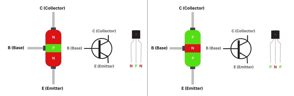
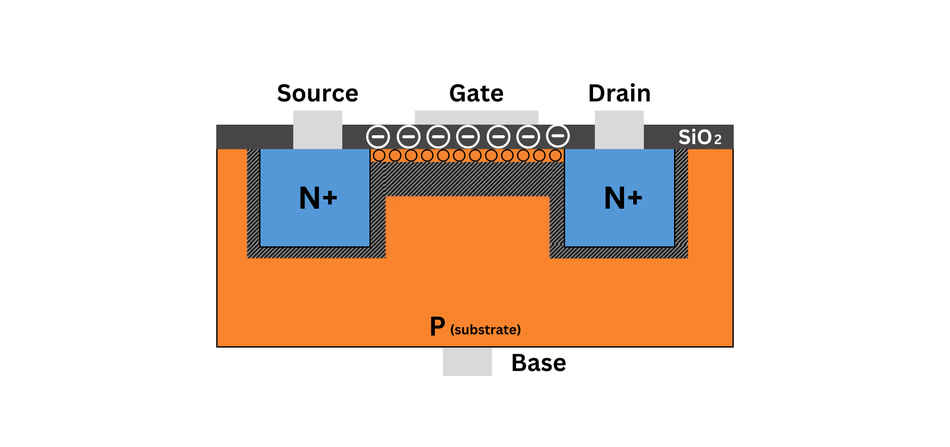
MOSFET is fundamentally a four-layer structure, combining metal, oxide, and semiconductor materials to create a highly efficient, controllable electronic switch. Understanding the physical structure behind the symbol clarifies how MOSFETs work.
In a planar n-channel MOSFET, two heavily doped n-type regions form the source and drain, embedded into a p-type substrate. Over the region between them lies a thin silicon dioxide layer, acting as the dielectric between the metal gate and the channel region. This oxide functions like a capacitor, separating the gate electrically while allowing the electric field to influence the charge carriers in the semiconductor below.
Once a positive gate-source voltage (VGS) is applied, the electric field repels holes (the majority carriers in the p-type substrate) and attracts electrons, forming a thin inversion layer of mobile electrons just beneath the oxide interface. This inversion channel bridges the source terminal and drain terminal, enabling current flow when a drain-source voltage (VDS) is present. The direction of electron conduction in an n-channel MOSFET runs from source to drain, opposite to the conventional current direction.
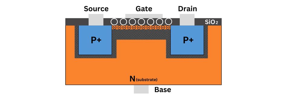
For a p-channel MOSFET, the polarity is reversed. The substrate is n-type, while the source and drain are p-type regions. Applying a negative gate voltage creates a p-type inversion layer, allowing hole conduction through the channel. The arrow orientation in the MOSFET symbol accurately represents this polarity—inward for NMOS and outward for PMOS—providing instant visual distinction in circuit schematics.
In enhancement-mode MOSFETs, no conduction occurs at zero gate bias because the channel doesn’t exist until the threshold voltage (VGS(th)) is reached. By contrast, depletion-mode MOSFETs contain a pre-doped channel, allowing current to flow even when the gate voltage is zero. Applying a reverse gate-source voltage depletes the charge carriers of the channel, effectively modulating or stopping conduction. This difference explains why enhancement-mode types dominate digital logic, while depletion-mode devices are often found in analog amplifiers or biasing circuits.
The key electrical parameters include:
| Parameter | Description and Typical Values |
| VGS(th) | The gate-source voltage required to form a conducting channel. For logic-level n-channel MOSFETs, it ranges from 1–4 V; for p-channel MOSFETs, it is negative. Devices must exceed this threshold to turn on. |
| VDS(max) | The maximum drain-source voltage the device can safely withstand. Exceeding this value leads to avalanche breakdown and possible device failure. |
| RDS(on) | The on-state resistance between drain and source during conduction. Small-signal MOSFETs typically have 1–10 Ω, while power MOSFETs can achieve values below 1 mΩ, improving efficiency. |
| ID(max) | The maximum continuous drain current a MOSFET can handle, determined by die size, thermal dissipation, and package design. Power MOSFETs can handle tens to hundreds of amperes. |
| Gate Charge / Capacitance | Represents the total capacitance between the gate and channel. This determines how fast the MOSFET can switch on or off and directly impacts switching losses and the required gate drive strength. |
Because the gate oxide is extremely thin, MOSFET gates are sensitive to electrostatic discharge (ESD). Designers should avoid leaving gates floating and use gate‑to‑source resistors or protection diodes to prevent damage.
Recommended Reading: N-Channel MOSFET Basics: Theory, Operation and Practical Implementations
How MOSFETs Work?
Formation of the Conduction Channel
In an n-channel MOSFET, when the gate-source voltage (VGS) exceeds the threshold voltage (VGS(th)), electrons are attracted toward the semiconductor–oxide interface. This forms a conductive n-type channel connecting the source terminal and drain terminal. When a drain-source voltage (VDS) is applied, electrons drift from the source to the drain, producing a measurable drain current (ID).
For a p-channel MOSFET, the process is reversed: applying a negative gate voltage attracts holes, creating a p-type inversion layer. [3] The arrow orientation in the MOSFET symbol reflects this — pointing inward for NMOS and outward for PMOS, indicating the direction of charge carrier flow (from P-type to N-type).
The magnitude of drain current depends on VGS, VDS, and the physical dimensions of the transistor, particularly the channel width-to-length ratio (W/L). This ratio is a key design parameter in both discrete and integrated circuits, determining conduction strength, speed, and power efficiency.
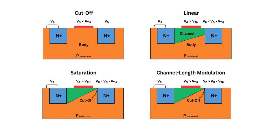
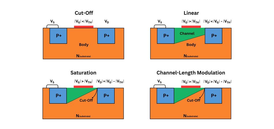
Operating Regions of MOSFETs
The MOSFET can operate in three primary regions, depending on VGS and VDS bias conditions:
Cutoff Region: The channel is not formed, and no drain current flows. The MOSFET behaves like an open switch. Both enhancement-mode and depletion-mode devices can enter this state if the gate voltage is sufficiently low or reversed.
Ohmic or Linear Region: A conductive channel exists between drain and source, and the MOSFET acts like a variable resistor. Here, current flow increases linearly with VDS, making this region useful for analog applications such as amplifiers and analog switches. Designers often compare this behavior to that of a resistor whose value is controlled by VGS.
Saturation (Active) Region: The channel near the drain end becomes pinched off, and drain current levels off to a constant value, controlled primarily by VGS. This region is crucial for digital switching and signal amplification, where stable current conduction is desired.
Mathematically, in this region:
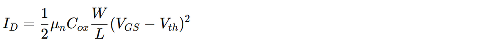
where μₙ is the electron mobility, and Cox is the gate oxide capacitance per unit area. This quadratic relationship forms the foundation for MOSFET-based amplifiers, current mirrors, and CMOS logic circuits.
Capacitance and Switching Characteristics
The gate of a MOSFET behaves as a capacitor, storing charge between the metal gate and the semiconductor channel. During operation, this capacitance (CGS, CGD, CDS) governs how fast the device can turn on and off:
The larger gate capacitance requires more charge (Qg), increasing the switching time and power dissipation.
Logic-level NMOS transistors typically exhibit lower gate charge for faster response, while power MOSFETs sacrifice speed for higher current capacity.
The product of VGS, CGS, and switching frequency defines the dynamic power loss, a key consideration in high-speed power electronics and DC–DC converters.
Recommended Reading: How Do MOSFETs Work: Comprehensive Technical Guide for Engineers (2025)
Reading and Interpreting MOSFET Symbols
Identifying Terminals when Labels are Absent
Many schematics omit labels on the MOSFET symbol, expecting the reader to infer the terminals:
Look at the Arrow: The arrow is drawn on or near the body. For three‑terminal symbols, it is connected to the source; for four‑terminal symbols the body lead is separate. If the arrow points inward, the device is NMOS; if outward, it is PMOS.
Check the Channel Line Style: A broken line means enhancement mode and a solid line means depletion mode.
Distinguish Gate, Drain and Source: The gate is always drawn offset from the channel and separated by a gap. The remaining two terminals at either end of the channel are the source and drain; the one connected to the arrow (or body) is the source.
Beware Symmetrical Devices: Planar MOSFETs are physically symmetrical, so the source and drain can swap roles. However, data sheets often specify one pin as the drain for ease of description, and the intrinsic diode orientation matters.
Example: NMOS enhancement transistor
The typical NMOS enhancement transistor symbol shows a dashed channel line and an arrow on the body pointing inward. The gate is separated by a dielectric gap.
In this configuration, no drain current flows when VGS = 0, as the channel does not yet exist. When VGS rises above the threshold voltage (2–4 V typical), a conductive inversion layer forms, allowing electrons to flow from source to drain. Conventionally, current flow is defined from drain to source, opposite to electron motion.
In a p-channel MOSFET, this behavior is inverted: current flows when the gate-source voltage is sufficiently negative, and the arrow points outward, indicating hole conduction within a p-type channel.
Example: Depletion‑mode JFET‑like MOSFET
The depletion-mode MOSFET is drawn with a solid channel line, symbolizing a pre-doped conductive path between drain and source.
In a depletion-mode NMOS, current flows even at zero gate bias. Applying a negative gate-source voltage (VGS) repels electrons, depleting the channel and reducing drain current. At a sufficiently negative VGS, the channel pinches off, and conduction stops.
A depletion-mode PMOS operates similarly but with reversed polarity, using hole depletion instead of electron depletion, and an arrow pointing outward in the MOSFET symbol.
These JFET-like MOSFETs are valuable in analog bias networks, constant-current sources, and voltage reference circuits, where a normally-on device simplifies biasing. They are less common than enhancement-mode types, but remain useful in specialized low-noise amplifiers and high-impedance measurement systems.
Recommended Reading: JFET vs MOSFET: A Comprehensive Engineering Analysis and Selection Guide
Practical Design Considerations
Selecting a MOSFET for Switching Applications
When choosing a MOSFET, engineers must consider several factors:
Voltage and Current Ratings: Ensure VDS(max) exceeds the supply voltage with adequate margin and ID(max) meets the load requirement.
RDS(on) and Power Dissipation: Low on‑resistance reduces conduction losses. Use the RDS(on) value at the expected gate drive voltage; logic‑level devices specify RDS(on) at 4.5 V or 2.5 V.
Gate Drive Capability: Large MOSFETs have significant gate charge; driving them quickly requires gate drivers capable of sourcing and sinking high currents.
Switching Speed and Capacitances: High‑frequency converters need low gate‑to‑drain (Miller) capacitance to minimize switching losses.
Package and Thermal Considerations: Surface‑mount packages (e.g., SO‑8, DPAK) handle different power levels. Evaluate thermal resistance and plan for heat sinking.
For logic-level switching, small NMOS devices can directly interface with microcontroller outputs provided that the gate threshold and RDS(on) meet requirements.
High‑side switching often uses P‑channel MOSFETs for simplicity; however, P‑channel devices generally have higher RDS(on) than equivalent N‑channels. Alternatively, designers use N‑channel MOSFETs with gate‑driver ICs that generate a gate voltage above the supply. In half‑bridge and full‑bridge converters, complementary NMOS devices are paired, and the body diode provides a path for freewheeling currents—although Schottky diodes or synchronous rectification may improve efficiency.
High-Side and Low-Side Switching
In low-side switching, n-channel MOSFETs are preferred due to their low RDS(on), high electron mobility, and cost efficiency. They connect the load between the positive supply and the drain terminal, with the source grounded.
For high-side switching, designers often choose p-channel MOSFETs for simplicity, since the source connects directly to VDD and a negative VGS turns the device on. However, p-channel MOSFETs typically have higher on-resistance and lower current capability than their n-channel counterparts.
Modern systems instead use n-channel MOSFETs driven by bootstrap or charge-pump gate driver ICs, generating a gate voltage above the supply. This allows complementary NMOS pairs in half-bridge or full-bridge converters. The body diode within each MOSFET naturally provides a freewheeling current path, though external Schottky diodes or synchronous rectification can improve efficiency and thermal reliability.
Protection Circuits and Reliability
MOSFETs can fail due to overvoltage, overcurrent or overheating. The key protection techniques include:
Gate Protection: Add a zener diode between gate and source to clamp the gate voltage below VGS(max). Use resistor networks or RC snubbers to damp voltage spikes and prevent gate oscillation.
Flyback Diodes and Freewheeling: When driving inductive loads, connect a diode (often the intrinsic body diode) across the load to provide a current path when the MOSFET turns off. For high current, use external Schottky diodes.
Current Limiting and Thermal Shutdown: Incorporate sense resistors and control circuitry to limit current. Many driver ICs include under‑voltage lockout and thermal shutdown.
ESD Precautions: Handle MOSFETs with grounded wrist straps and use protective packaging. In circuits, tie unused gates to ground or supply through resistors to avoid static buildup.
MOSFETs in Analog Design
While the MOSFET symbol is often associated with digital switching and CMOS logic, the Field Effect Transistor (FET) also plays a crucial role in analog electronics:
In transconductance amplifiers, a MOSFET converts input voltage into output current, leveraging its gate-controlled conduction.
When operated in the ohmic region, it functions as a voltage-controlled resistor, ideal for analog volume controls and variable gain amplifiers.
Depletion-mode MOSFETs are often used as constant-current sources due to their naturally on-state conduction.
MOS capacitors, formed by the gate oxide and substrate, are key elements in analog switches, sample-and-hold circuits, and filter networks.
In these analog contexts, understanding the MOSFET symbol, substrate polarity, and biasing scheme ensures accurate interpretation of circuit schematics and proper device selection. The balance between linearity, impedance, and thermal performance remains central to analog MOSFET design.
Evolution: FinFETs, Wide‑Bandgap MOSFETs and Beyond
FinFETs versus Planar MOSFETs
Traditional planar MOSFETs consist of a flat, horizontally oriented channel beneath the gate oxide, where electrons (in an n-channel MOSFET) or holes (in a p-channel MOSFET) flow between the source and drain. As transistor geometries shrank below 45 nm, this two-dimensional design began to struggle with short-channel effects, leakage, and threshold voltage instability.
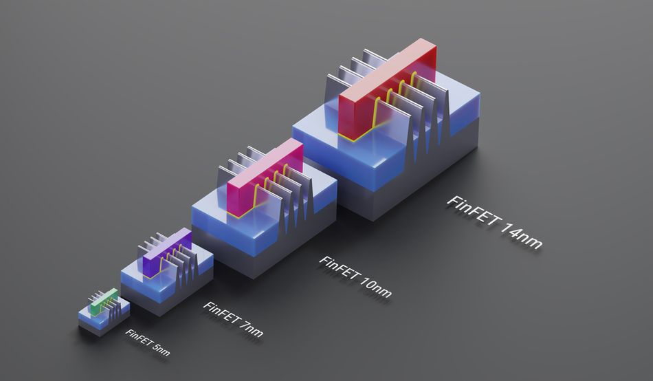
FinFETs (Fin Field-Effect Transistors) introduced a breakthrough by adding a vertical fin of silicon that protrudes from the substrate, wrapping the gate terminal around multiple sides of the channel. [4] This three-dimensional geometry provides far stronger electrostatic control, minimizing leakage and improving current flow uniformity.
The FinFET symbol sometimes appears as a double-gate MOSFET symbol, but in most schematic diagrams, engineers continue to use the standard MOSFET symbol, focusing on function rather than structure. Despite their similar appearance, FinFETs offer substantial advantages that include better channel control, reduced short-channel effects, lower leakage current, higher drive current density, faster switching speed and improved scalability.
However, FinFETs bring challenges: quantized fin widths, complex fabrication, and higher manufacturing costs. Despite these trade-offs, FinFETs dominate advanced CMOS nodes (28 nm and below) used in processors, GPUs, and high-speed communication ICs. For these applications, the superior gate control and energy efficiency of FinFET outweigh its fabrication complexity.
Wide‑Bandgap MOSFETs: SiC and GaN
Beyond structural evolution, new semiconductor materials are redefining the power electronics landscape. Wide-bandgap (WBG) materials such as silicon carbide (SiC) and gallium nitride (GaN) offer dramatic performance gains over conventional silicon MOSFETs.
SiC MOSFETs possess a bandgap approximately three times larger than silicon, enabling higher breakdown voltages, lower RDS(on), and operation at elevated temperatures. Their ability to maintain stable conduction under high voltage and thermal stress makes them ideal for electric vehicles, renewable energy systems, and industrial drives.
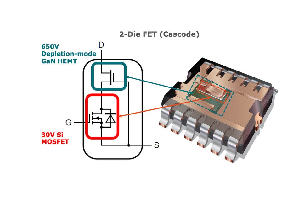
GaN MOSFETs, often implemented as high-electron-mobility transistors (HEMTs), take performance even further. Their high electron mobility and low charge storage enable ultra-fast switching, reduced gate charge, and minimal switching losses. These characteristics allow compact, high-frequency converters with unprecedented efficiency and power density.
Both SiC and GaN devices are typically enhancement-mode MOSFETs, sharing the same schematic symbol as their silicon counterparts. However, engineers must interpret datasheet parameters carefully, as threshold voltage, gate charge, and capacitance values differ significantly from traditional silicon devices.
Market Trends and Statistics (2024–2032)
Recent data illustrates the accelerating global shift toward power MOSFET adoption and wide-bandgap integration:
The global power MOSFET market was valued at US$27.53 billion in 2024 and is projected to reach US$48.40 billion by 2032, a CAGR of 7.34 %.
Enhancement‑mode MOSFETs dominated the market in 2024 with 78.4% share, reflecting their prevalence in switching and digital applications.
The high‑power segment held 40.8% share thanks to EVs, renewables and industrial systems, while the automotive sector accounted for 27.2% of total demand.
Asia–Pacific led with 41.5% share and continues to grow due to industrialization, EV production and 5G/IoT deployment. North America is expanding because of SiC/GaN adoption and renewable energy, and Europe’s growth is driven by energy efficiency regulations.
The future points toward nanosheet FETs, gate-all-around transistors, and 2D-material MOSFETs built from graphene or MoS₂, promising even higher carrier mobility and reduced capacitance. Their structures may differ, but circuit diagrams will likely continue to employ the familiar MOSFET symbol, a lasting graphical language linking decades of semiconductor innovation.
Recommended Reading: Extending the Battery Life of Hearables and Wearables with Single-Inductor Multiple-Output Switching Architecture
Conclusion
The MOSFET symbol may look simple, but it encodes a wealth of information about a transistor’s type, mode and physical behavior. By understanding the channel line style, arrow orientation, and body connection, engineers can quickly determine whether a device is n-channel or p-channel, enhancement or depletion, and how it will conduct in a circuit. The intrinsic body diode and parasitic structures influence switching behavior and must be considered in designs.
In the broader context, MOSFETs continue to evolve. FinFETs and other 3‑D devices address the limitations of planar MOSFETs at nanometer scales, while SiC and GaN MOSFETs push power devices toward higher efficiency and faster switching. With the global power MOSFET market forecast to surpass US$48 billion by 2032, engineers who understand the intricacies of MOSFET symbols and characteristics will remain at the forefront of digital design, power electronics and emerging technologies.
Frequently Asked Questions (FAQs)
1. What do the gate, drain and source terminals represent in a MOSFET symbol?
A. The gate in this voltage-controlled device regulates conductivity, while electrons enter at the source and exit through the drain. On a PCB, the gate is insulated from the channel by an oxide gap.
2. How can I distinguish n‑channel and p‑channel MOSFET symbols?
A. The arrow direction identifies MOSFET types—inward for n-channel MOSFETs, outward for p-channel MOSFETs. The internal diode orientation also differs, much like npn and pnp junctions in a bipolar junction transistor.
3. Why is the channel line broken in some MOSFET symbols?
A. A broken (dashed) channel line denotes an enhancement‑mode MOSFET, which is normally off and requires a gate‑source voltage to form a channel. A solid line denotes a depletion‑mode MOSFET that is normally on.
4. What is the intrinsic body diode, and how is it shown?
A. The intrinsic diode between body and drain conducts during reverse current flow. It appears parallel to the channel, following the arrow pointing direction defined by device polarity on circuit PCBs.
5. How do FinFETs differ from MOSFETs, and does the symbol change?
A. FinFETs use a vertical emitter-like fin surrounded by the gate, offering better electrostatic control. The MOSFET symbol remains unchanged since circuit behavior resembles conventional field-effect transistor operation.
References
[1] Wevolver. PMOS vs NMOS: Unraveling the Differences in Transistor Technology [Cited 2025 October 21] Available at: Link
[2] ResearchGate. Advancements And Applications of Field-Effect Transistors in Modern Electronics [Cited 2025 October 21] Available at: Link
[3] Wevolver. N-Channel MOSFET Basics: Theory, Operation and Practical Implementations [Cited 2025 October 21] Available at: Link
[4] ResearchGate. Review on Fin Shape Channel Field Effect Transistor (FinFET) [Cited 2025 October 21] Available at: Link
in this article
1. Introduction2. Anatomy of the MOSFET symbol3. Physical Construction and Operation4. How MOSFETs Work?5. Reading and Interpreting MOSFET Symbols6. Practical Design Considerations7. Evolution: FinFETs, Wide‑Bandgap MOSFETs and Beyond8. Conclusion9. Frequently Asked Questions (FAQs)10. References