N-Channel MOSFET Basics: Theory, Operation and Practical Implementations
This article explores the theory, operation, and real-world implementations to provide a comprehensive understanding of N-Channel MOSFET basics for professional engineers and advanced learners.

Last updated on 16 Sep, 2025. 17 minutes read
Key Takeaways
What is a N‑channel MOSFET? The NMOS transistor uses a p‑type substrate with n+ source and drain regions. Once a positive gate‑to‑source voltage exceeds the threshold voltage, electrons accumulate under the gate oxide to form a conductive channel.
Operating Modes: NMOS devices operate in three modes—cut‑off, triode (linear), and saturation, depending on gate and drain voltages. Understanding the conditions for each mode and the corresponding current equations is vital for circuit design.
Why NMOS is Preferred? Electrons have higher mobility than holes, so N‑channel MOSFETs switch faster and exhibit lower on‑state resistance than P‑channel devices. However, a positive gate voltage is required, and high‑side switching often needs a gate driver.
Key Parameters: Threshold voltage (typically 0.5–1 V for logic‑level NMOS), transconductance, drain current, and output conductance determine performance. Proper selection of these parameters enables the design of low-power, high-speed systems.
Applications and Trends: NMOS transistors are ubiquitous in logic, analog, and power circuits. Market data indicate a rising demand for medium- and low-voltage MOSFETs in power conversion, automotive, and consumer electronics, driven by innovations in SiC/GaN technologies.
Introduction
In modern electronics, N-channel MOSFET basics represent a fundamental building block for efficient power management and signal control. These devices are widely used in switching applications, amplifiers, and motor drivers due to their superior conduction properties compared to P-channel MOSFETs. Understanding the N-channel MOSFET basics is essential for engineers seeking to optimize circuit performance, as they operate with low on-resistance and high-speed switching capabilities. This makes them useful in areas such as embedded systems, renewable energy solutions, and consumer electronics.
By mastering the basics of NMOS, designers can implement cost-effective, reliable, and scalable solutions across both low-power and high-power systems. Furthermore, practical applications, from DC-DC converters to RF circuits, highlight the versatility of these components. This article explores the theory, operation, and real-world implementations to provide a comprehensive understanding of N-channel MOSFET basics for professional engineers and advanced learners.
MOSFET Fundamentals
Brief History and Significance
The metal-oxide-semiconductor field-effect transistor (MOSFET) was first demonstrated by Mohamed Atalla and Dawon Kahng at Bell Labs in 1959. [1] This invention fundamentally transformed electronics by enabling miniaturization, low power consumption, and large-scale integration. Unlike the Bipolar Junction Transistor (BJT), which requires continuous base current, the MOSFET relies on an insulated gate terminal, allowing voltage control with negligible input current. By the mid-1970s, MOSFETs dominated digital logic, powering microprocessors and memory chips.
Today, over 100 billion MOSFET transistors are fabricated annually, making them the most widely manufactured electronic device in history. Their scalability, energy efficiency, and ability to integrate into CMOS technology cemented their role as the foundation of modern computing and power electronics.
Structure of an NMOS Transistor
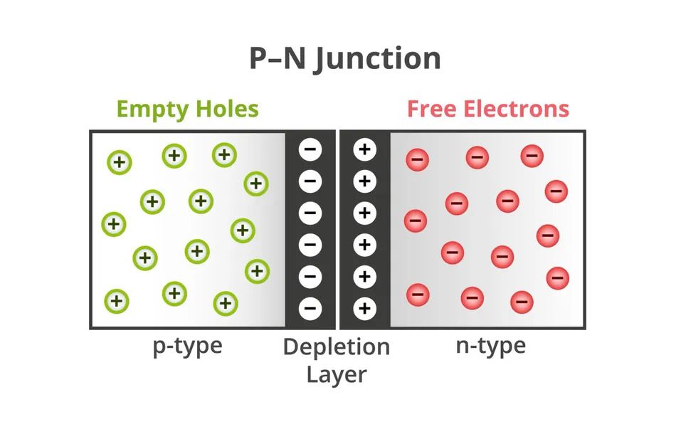
The enhancement-mode N-channel MOSFET is fabricated on a p-type silicon substrate with two heavily doped n+ regions forming the source terminal and drain terminal. One thin layer of silicon dioxide (SiO₂) separates the metal gate from the substrate, creating a high-impedance MOS capacitor. [2] This unique structure allows electric fields to modulate conductivity in the underlying substrate without direct current injection.
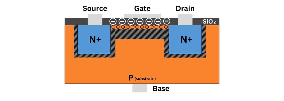
When unbiased, the p-type substrate prevents conduction since no electron channel exists between the source and drain. Applying a positive Gate Source Voltage (VGS) generates an electric field that attracts electrons, forming an n-type inversion layer beneath the oxide. This effectively creates an N → N → N conduction path, enabling current flow.
The threshold voltage (VTH or Vth) is a key parameter defined as the minimum VGS needed to induce a conductive inversion channel. In logic-level NMOS devices, VTH typically ranges between 0.5 V and 1 V, enabling direct interfacing with microcontrollers and low-voltage circuits. Below this threshold, the MOSFET remains in cut-off, allowing only a minute subthreshold current to pass.
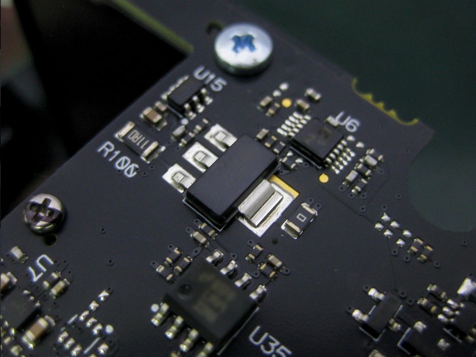
Datasheets and tutorials for power MOSFET devices specify additional characteristics such as RDS(on) (on-resistance), maximum VDS (drain-source voltage), and safe operating areas, which are crucial in power supplies, amplifiers, and motor control applications.
The NMOS structure: p-type substrate, n+ regions, insulated gate, and inversion channel provides precise control of conduction, making it indispensable for both digital and power applications.
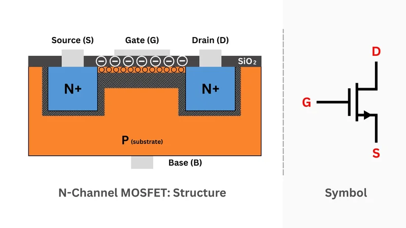
Diagram of Cross-Section and Symbol
The NMOS transistor cross-section provides a visual representation of its fundamental structure. Built on a p-type substrate, it contains two heavily doped n+ regions functioning as the drain terminal and source terminal. A thin layer of silicon dioxide serves as the insulating medium, separating the metal gate from the underlying substrate. This oxide layer plays a vital role in channel formation, as it allows the electric field from the gate to influence the semiconductor surface without direct current flow.
When the gate-source voltage (VGS) exceeds the threshold voltage (VTH or Vth), an n-type inversion channel is induced beneath the gate. This conductive path enables electron conduction from source to drain, with current flow governed by VDS. In circuit symbols, an arrow denotes the body or substrate connection, which in discrete devices is typically shorted to the source. Additionally, the intrinsic body diode between the drain and source is an inherent feature, critical for power MOSFET applications such as motor control and power supplies.
The NMOS cross-section and symbol highlight its insulated control mechanism, intrinsic diode, and channel formation, forming the basis for understanding how a MOSFET works.
Recommended Reading: How Do MOSFETs Work: Comprehensive Technical Guide for Engineers (2025)
NMOS Operation and Modes
Formation of the Channel and Role of the Threshold Voltage
In an N-channel MOSFET, the gate terminal modulates channel formation through a capacitive coupling effect. When a positive voltage is applied between the gate and source, an electric field develops across the thin silicon dioxide layer, repelling holes from the p-type substrate and attracting free electrons to the surface. Once the gate-source voltage (VGS) surpasses the threshold voltage (VTH or Vth), the surface potential bends the bands enough to form an n-type inversion channel. This conductive path bridges the drain terminal and source terminal, enabling conduction.
The drain current (ID) is influenced by both VGS and the drain-to-source voltage (VDS). As per MIT’s device physics notes, the inversion charge density is set by VGS, while VDS determines carrier drift velocity along the channel. Consequently, increasing VGS or VDS raises the current flow until saturation is reached, where further increases in VDS have a negligible effect on ID.
Cut-off, Triode, and Saturation Modes
The figure below illustrates the cross-sectional behavior of an N-channel MOSFET across its primary modes of operation:
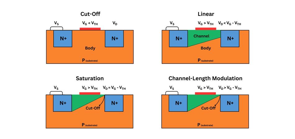
1. Cut-Off Mode (VG < VTH):
With the gate voltage below the threshold voltage, no inversion channel forms. The p-type substrate blocks conduction between the source and drain, resulting in only leakage current.
The approximate current expression is:

2. Linear (Triode) Mode (VG > VTH, VD < VG – VTH):
Applying a gate voltage greater than VTH induces an n-type inversion channel beneath the gate. As VDS increases, electrons drift from source to drain. Current rises nearly linearly with VDS, and the MOSFET behaves like a variable resistor.
The approximate current expression is:

3. Saturation (Active) Mode (VG > VTH, VD = VG – VTH):
At higher drain voltages, the channel pinches off near the drain side. Conduction continues, but the drain current becomes nearly independent of VDS, depending mainly on VGS. This is the preferred region for amplifiers and analog circuits.
The approximate current expression is:

4. Channel-Length Modulation (VG > VTH, VD > VG – VTH):
Beyond saturation, increasing VDS shortens the effective channel length. This effect, known as channel-length modulation, causes a slight increase in drain current with VDS, similar to the Early effect in BJTs. It is especially relevant in analog MOSFET design and must be accounted for in precision circuits.
In saturation with channel-length modulation, the drain current is modelled as:

This captures the physical changes inside the MOSFET for different operating regions, bridging theoretical equations with practical device behavior.
Body Diode and Body Effect
Due to the p–n junctions between the n+ regions and the p-type substrate, an NMOS transistor inherently includes a body diode. In discrete power MOSFET designs, the substrate is shorted to the source terminal, creating a diode between the source and drain (anode at the source, cathode at the drain). This intrinsic diode conducts when the drain becomes more negative than the source, providing a critical path in motor control, PWM applications, and power supplies.
The body effect describes how the source-to-body voltage alters the threshold voltage. An elevated source potential increases VTH, reducing current drive capability. While discrete devices usually tie the body to the source to suppress this, in CMOS integrated circuits, the body may be independently biased, allowing threshold adjustment and performance tuning.
The intrinsic body diode ensures reverse current flow capability, while the body effect highlights substrate biasing’s role in shaping device threshold voltage and current drive.
Recommended Reading: N-Type Vs P-Type: Difference Between P-Type and N-Type Semiconductors
NMOS vs PMOS and Why N‑channel Devices Dominate
Carrier Mobility and On-State Resistance
The defining difference between NMOS and PMOS devices is their charge carriers. NMOS transistors rely on electrons, while PMOS transistors conduct via holes. Since electron mobility in silicon is approximately 2–3 times higher than hole mobility, NMOS transistors achieve significantly higher current densities for the same gate-source overdrive and geometry. [3] This translates into lower on-state resistance (RDS(on)), improved conduction efficiency, and faster switching speeds.
Consequently, a PMOS transistor must be nearly 2 - 3 times larger than an NMOS device to achieve a comparable RDS(on), increasing die size and cost. Power electronics studies confirm that NMOS devices dominate in low-RDS(on) power MOSFET applications, such as DC-DC converters and motor control systems.
Threshold Voltage Polarity
The threshold voltage (VTH) polarity distinguishes NMOS and PMOS switching behavior. NMOS devices turn on when a positive gate-to-source voltage exceeds VTH (typically +0.5 to 1 V in logic-level MOSFETs). Conversely, PMOS devices activate when a negative gate-source voltage crosses their negative threshold voltage, often around –0.5 to –1 V. This polarity difference has significant implications in circuit design.
For high-side switching, a PMOS MOSFET can be directly driven from the supply rail, whereas an NMOS requires a gate voltage above VDD, which is often implemented using a bootstrap circuit or charge pump. PMOS transistors remain favoured for simple high-side designs, despite their higher resistance.
Complementary use in CMOS
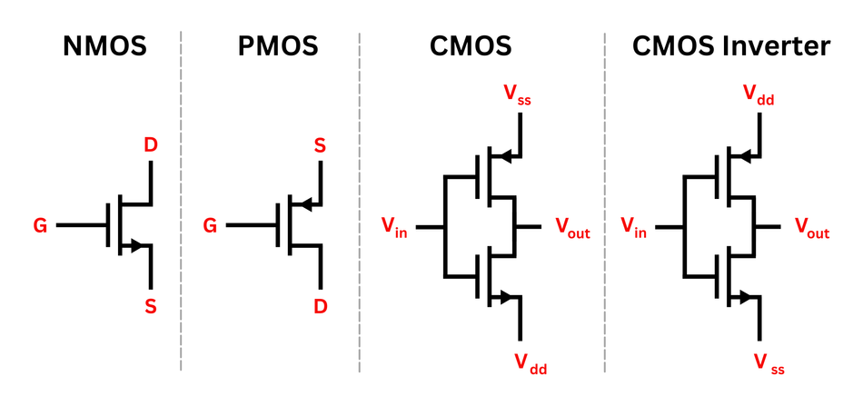
Despite NMOS advantages in speed and current drive, CMOS technology leverages the complementary pairing of NMOS and PMOS devices to minimize power. In CMOS logic, an NMOS pulls outputs low, while a PMOS pulls them high, eliminating direct supply-to-ground conduction paths during steady states. This configuration enables near-zero static power dissipation, full rail-to-rail output swings, and compact transistor layouts.
Since its adoption in the late 1970s, CMOS has replaced NMOS-only logic families, driving advances in microprocessors, memory chips, and SoCs. Today, advanced nodes pack billions of NMOS and PMOS transistors side by side, with ongoing innovations in FinFET and GAA FET architectures extending CMOS scaling beyond 3 nm.
CMOS technology balances NMOS drive strength with PMOS efficiency, providing unmatched scalability, energy efficiency, and dominance in modern digital and mixed-signal integrated circuit design.
Recommended Reading: PMOS vs NMOS: Unraveling the Differences in Transistor Technology
Key Parameters and Device Characteristics
Threshold Voltage (VTH)
The threshold voltage (VTH) is the minimum gate-to-source voltage (VGS) required to create an inversion channel. Its value depends on substrate doping concentration, oxide thickness, and gate electrode material. Lower VTH values allow faster switching, but they also increase sub-threshold leakage current, especially in scaled devices. Logic‑level NMOS transistors commonly used with 3.3 V or 5 V microcontrollers have thresholds in the 0.5 to 1 V range.
For power MOSFETs, thresholds may range from 2 to 4 V. Designers should consult the datasheets for both the minimum threshold (where the device begins to conduct) and the recommended gate voltage for full enhancement.
Transconductance (gm)
Transconductance (gm) measures how effectively a MOSFET converts gate voltage variations into drain current, mathematically defined as:
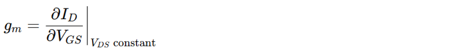
It is proportional to electron mobility (µn), oxide capacitance per unit area (Cox), and the W/L ratio of the channel. A higher gm means a slight change in VGS produces a significant change in drain current, making high-gm devices especially useful in analog amplifiers and high-gain circuits. Temperature and channel scaling significantly impact gm, with shorter channels generally yielding higher transconductance.
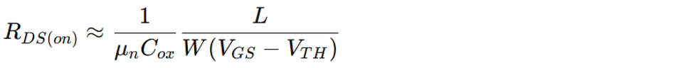
Drain Current (ID) and On-State Resistance (RDS(on))
The drain current (ID) depends on VGS, VDS, and MOSFET geometry. In the linear region, ID rises with VDS until it reaches saturation. In power switching, the on-state resistance (RDS(on)) is critical, as it represents the effective resistance between drain-source under full conduction.
The lower RDS(on) minimizes conduction losses, improves power supply efficiency, and reduces device heating. Due to higher electron mobility, NMOS devices achieve significantly lower RDS(on) for a given area than PMOS, which is why N-channel power MOSFETs dominate in high-efficiency converters.
Gate Charge (QG) and Switching Speed
The total gate charge is the amount of charge that must be transferred to and from the gate to switch the MOSFET. It is the integral of gate capacitance over voltage and determines how quickly a driver can turn the transistor on or off.
Lower gate charge leads to faster switching and lower gate‑drive losses. Designers must ensure the gate driver can supply the required current to charge the gate capacitance rapidly.
Output Conductance and Channel-Length Modulation
Ideally, a MOSFET in saturation mode acts as a current source independent of VDS. In practice, channel-length modulation reduces output resistance, producing finite output conductance. This effect is expressed by the channel-length modulation parameter (λ) and becomes significant as devices scale down.
The high output conductance leads to reduced gain in analog amplifiers and distortion in linear circuits. Minimizing this parameter through device engineering or circuit techniques such as cascode configurations improves linearity and current-source behavior.
Channel-length modulation introduces non-ideality; minimizing output conductance is essential for precision in analog amplifiers and stable MOSFET current-source implementations.
Recommended Reading: Concurrent-Mode CMOS Detector IC for Sub-Terahertz Imaging System
Operating Modes: Equations and Practical Implications
Cut-Off Region
In the cut‑off region, no inversion channel forms, and the MOSFET remains effectively non-conductive. The drain current is nearly zero except for leakage and sub-threshold conduction, both of which increase with temperature and device scaling.
In practical design, this region corresponds to the MOSFET acting as an open switch. In ultra-low-power systems, leakage currents must be considered to avoid excessive standby power consumption, especially in deep submicron CMOS nodes.
Triode (Linear) Region
When VGS > VTH and VDS < VGS − VTHV, the channel extends across the full device, behaving as a voltage-controlled resistor. Using the charge-control model, the drain current is proportional to both gate overdrive (VGS−VTH) and VDS:

For small VDS, the on-resistance is approximated as:
This region is crucial for analog switches, resistive loads, and source-degeneration amplifiers, where the MOSFET mimics a controlled resistor.
Saturation region
As VDS rises, the channel pinches off near the drain when VDS ≥ VGS − VTH. Beyond this point, current saturates and becomes weakly dependent on VDS. The classic square-law model for long-channel devices is:

This approximation holds for long‑channel devices. In modern short‑channel MOSFETs, velocity saturation and drain‑induced barrier lowering modify the I–V characteristics.
Body Diode Conduction
The intrinsic body diode becomes important in power applications, especially in synchronous rectifiers and motor drives. When an NMOS is reverse‑biased (drain at a lower potential than source), the body diode conducts and clamps the voltage.
Designers often use this diode intentionally, for example, a free‑wheel path in buck converters, but must ensure it can handle reverse recovery losses. Some MOSFETs incorporate a fast body diode; others use an external Schottky diode to reduce losses.
Applications of N‑Channel MOSFETs
Digital Logic and CMOS
NMOS transistors were originally used alone to implement logic gates (NMOS logic). However, NMOS logic consumes static power because current flows when a gate outputs a logic low. Today, CMOS technology, combining NMOS and PMOS devices, dominates digital circuits.
In CMOS inverters, an NMOS transistor pulls the output to ground when the input is high, while a PMOS transistor pulls the output to the supply when the input is low. This complementary arrangement results in negligible static power dissipation.
Analog Circuits
In analog applications, NMOS devices function as transconductance elements in amplifiers, source followers, and current mirrors. Their high gm, low noise, and superior conduction characteristics make them ideal for op-amp input pairs and RF front ends.
Modern CMOS op-amps rely on NMOS input stages for high gain and wide bandwidth, with careful biasing to suppress threshold voltage variation. NMOS devices provide high transconductance, bandwidth, and low noise, making them indispensable in analog and RF circuit design. [4]
Low‑Side Switching
One common use of NMOS devices is as low‑side switches controlling loads connected between the drain and supply. In this configuration, the source is tied to ground (or the negative supply). Once a positive gate voltage greater than the threshold is applied, the MOSFET turns on and current flows from the load into ground.
This configuration is popular in power supplies, Arduino-based controls, and motor drivers, due to its simplicity and the blocking action of the intrinsic body diode in the off-state. Low-side switching is simple because the gate voltage only needs to exceed the threshold, and the body diode is oriented to block current from the load to the supply when the device is off.
High-Side Switching
High‑side switching places the MOSFET between the supply and the load. For an NMOS device, turning the transistor fully on requires the gate voltage to be higher than the supply by at least the threshold voltage. Driving an N‑channel MOSFET as a high‑side switch is complicated; a gate driver or charge pump is needed to generate the required gate overdrive.
P‑channel MOSFETs simplify high‑side switching because a negative gate bias relative to the source turns them on, eliminating the need for a charge pump. NMOS high-side control offers efficiency advantages but requires gate drivers or charge pumps, unlike PMOS solutions, which simplify biasing.
Analog Switches
NMOS transistors appear in analog multiplexers and transmission gates, often paired with PMOS to reduce distortion. This arrangement ensures low on-resistance across the full voltage swing, enabling high-quality signal transfer in mixed-signal ICs, audio processing, and data acquisition systems. NMOS devices, paired with PMOS in transmission gates, ensure low-loss, wide-range analog switching in mixed-signal designs.
Power Electronics
In power conversion, NMOS devices handle high currents and voltages. Low-voltage N-channel MOSFETs switch DC loads in buck converters, synchronous rectifiers, and battery-protection circuits. Battery management and consumer electronics driving the demand have led to new NMOS products, such as a 30 V common‑drain N‑channel MOSFET by Toshiba for USB devices and battery pack protection.
N‑channel devices with enhanced thermal performance power electric vehicle (EV) powertrains, onboard chargers, and thermal-optimized power systems. Innovations in gallium nitride (GaN) and silicon carbide (SiC) MOSFETs are pushing switching frequencies higher and reducing losses. NMOS transistors dominate power electronics, driving efficiency in renewable energy, EVs, and consumer systems with Si, SiC, and GaN technology advancements.
Emerging NMOS technologies
While the basic structure of an NMOS has remained consistent, process innovations continue to improve performance. Trench MOSFETs use deep trenches to increase channel width and reduce on‑state resistance. Similarly, super‑junction MOSFETs balance n and p pillars to support high voltages while maintaining low resistance.
Wide‑bandgap materials such as SiC and GaN offer higher breakdown voltages and lower switching losses, enabling high‑frequency operation. These technologies are essential for EV chargers, renewable energy inverters, and data‑center power supplies.
Recommended Reading: NMOS and PMOS Transistors: Fundamentals and Applications
Design Considerations and Best Practices
Selecting an NMOS Device
When choosing an NMOS transistor for a design, engineers must consider:
Voltage Rating: The maximum drain-source voltage must exceed the highest voltage the device will experience during operation. Logic-level NMOS devices often range from 20–100 V, while power MOSFETs can withstand several hundred volts, especially in industrial and automotive power supplies.
Current Rating: The continuous and peak drain current should be adequate for the load. Package dissipation and heatsinking are crucial, as excessive thermal rise can degrade RDS(on) and long-term device reliability.
Threshold Voltage: For microcontroller-driven circuits, choose logic-level NMOS with VTH in the 0.5–1 V range. In noisy power environments, higher thresholds improve noise immunity and reduce false switching.
On‑State Resistance RDS(on): Lower RDS(on) improves conduction efficiency, reducing heat and power losses. However, extremely low RDS(on) often comes at the cost of a larger die area and higher device cost.
Gate Charge (QG): The total gate charge dictates switching speed. Lower QG supports high-frequency operation, but often increases RDS(on). Designers must balance these trade-offs to achieve efficiency and optimal switching performance.
Package and Thermal Characteristics: Packages such as TO‑220, TO‑247, DFN, and QFN offer different thermal resistances and footprints. The medium‑ and low‑voltage MOSFET market report highlights the dominance of TO‑220 packages due to their excellent thermal performance.
Careful NMOS selection requires balancing voltage, current, VTH, RDS(on), QG, and thermal packaging to achieve optimal performance, efficiency, and reliability in practical designs.
Gate Driving and Protection
Proper gate drive design is critical to achieve reliable NMOS operation:
Use a dedicated gate driver or buffer to supply sufficient current and voltage, especially in high-speed or high-power circuits.
A series gate resistor can damp oscillations, limit ringing, and tune rise/fall times.
Protective elements such as Zener diodes or TVS clamps safeguard the gate terminal from voltage spikes.
For inductive loads, manage drain-source overshoot and flyback energy. Snubbers, RC networks, or the intrinsic body diode provide essential protection against overvoltage stress.
Robust gate drive design, supplemented by protective elements, ensures NMOS transistors withstand voltage spikes, minimize ringing, and deliver consistent high-speed switching performance.
High-Side Switching Techniques
Driving an NMOS device in high-side configurations requires advanced techniques:
A bootstrap driver or charge pump must elevate the gate voltage above the supply by at least VTH to fully enhance conduction.
While P-channel MOSFETs simplify high-side switching, their higher RDS(on) limits efficiency. N-channel devices, when paired with the right driver, achieve lower losses and better current handling.
High-side NMOS designs are common in battery management, motor control, and synchronous converters where efficiency outweighs driver complexity.
High-side NMOS switches demand charge pumps or bootstrap drivers, but deliver superior efficiency and lower losses compared to PMOS alternatives.
Thermal management
NMOS power dissipation arises from both conduction losses and switching losses:
Conduction losses scale with load current squared, while switching losses grow with frequency and gate charge.
Ensure junction temperature remains within device limits by using appropriate heatsinks, thermal vias, or packages with exposed pads.
For compact designs, consider DFN/QFN packages with optimized thermal conductivity. In high-power systems, TO-247 or power modules offer better thermal headroom.
Effective thermal management, balancing conduction and switching losses with advanced packaging and cooling, ensures long-term NMOS reliability in power-dense designs.
Recommended Reading: Transistor as a Switch: Theory and Practical Implementation for Digital and Hardware Engineers
Market Trends and Industry Perspective
The global medium and low-voltage MOSFET market has been experiencing robust growth. The Global Power MOSFET Market was valued at USD 8.9 billion in 2024 and is projected to reach around USD 13.5 billion by 2030. [5] Power conversion applications accounted for the largest portion, about 34–35% of the market in 2024, followed closely by automotive electronics at approximately 32%. This demand is being fueled by the broader push for electrification: electric vehicles (EVs), renewable energy systems, and modern consumer electronics all require ever more efficient power management components.
Manufacturers continue to release new N-channel MOSFETs and related innovations to meet these growing needs, pushing the performance envelope, especially at higher power levels. Notably, wide-bandgap semiconductors such as silicon carbide (SiC) and gallium nitride (GaN) are enabling MOSFET devices with higher voltage capabilities and faster switching for high-frequency applications. The recent product developments illustrate this trend:
Toshiba (Nov 2023): Launched a 30 V common-drain N-channel MOSFET optimized for low-voltage, high-efficiency operation in USB power devices and battery pack protection systems. This device improves the safety and reliability of compact power management circuits.
ROHM (Sept 2024): Introduced a line of automotive-grade N-channel MOSFETs designed for high reliability in electric vehicle powertrains and battery management systems, offering enhanced thermal performance to meet stringent automotive requirements.
SemiQ (Jan 2025): Released 1700 V SiC MOSFETs aimed at high-voltage power conversion in aerospace, industrial, and renewable energy applications. These SiC-based transistors achieve high efficiency and can handle the demands of motor drives and inverter systems for clean energy.
Toshiba (May 2025): Unveiled its 3rd-generation 650 V SiC MOSFETs in a compact DFN8×8 package, targeting improved power density and efficiency for industrial power supplies, motor controllers, and EV inverter units. By leveraging SiC technology, these MOSFETs reduce switching losses and heat, benefiting high-power applications.
Vishay (May 2025): Introduced an 80 V N-channel MOSFET in an advanced PowerPAK 8×8 package, offering an industry-leading low RDS(on) for its class. This device is optimized for efficient power management in servers and industrial systems, minimizing conduction losses and supporting faster switching speeds.
The outlook for the MOSFET sector thus remains very promising, with ongoing technological advancements (like GaN and SiC devices) poised to enhance the efficiency of next-generation power electronics further.
Recommended Reading: Extending the Battery Life of Hearables and Wearables with Single-Inductor Multiple-Output Switching Architecture
Conclusion
N‑channel MOSFETs underpin modern electronics, from digital logic and analog circuits to power converters and electric vehicles. Their high electron mobility results in fast switching and low on‑state resistance, making them the preferred choice over P‑channel devices in most applications. Understanding the device structure, operating modes, key parameters, and circuit implications allows engineers to exploit NMOS performance while avoiding pitfalls such as body diode conduction or insufficient gate drive.
NMOS devices are now being complemented by wide‑bandgap semiconductors like SiC and GaN, yet the fundamental principles remain the same. With an awareness of market trends, emerging technologies and best practices, engineers can select and implement NMOS transistors to build efficient, reliable and future‑ready systems.
Frequently Asked Questions (FAQs)
Q. What is an N‑channel MOSFET and how does it work?
A. N-channel MOSFET (NMOS) is a solid-state device belonging to the field-effect transistor family. Structurally, it has an n+ source and drain diffused into a p-type substrate, with the MOSFET gate insulated by a thin oxide. When the gate-source voltage exceeds the threshold voltage, an n-type channel forms, allowing electrons to flow from the drain to the source. Below threshold, the device stays off, blocking conduction.
Q. What is the typical threshold voltage of an NMOS device?
A. The threshold voltage is the minimum VGS required to form an inversion channel. Logic-level NMOS devices often have thresholds of 0.5–1 V, while power MOSFETs may use 2–4 V thresholds. Datasheets provide exact values for design.
Q. What are the types of MOSFETs available?
A. There are two major types of MOSFET: enhancement type (normally off) and depletion mode (normally on). Most modern NMOS devices are n-channel enhancement MOSFETs used in switching and amplification. N-channel depletion devices are less common but useful in current regulation. For comparison, a JFET also relies on depletion but lacks an insulated gate.
Q. Why are N-channel MOSFETs preferred over P-channel devices?
A. Because electron mobility is about 2–3× higher than hole mobility, N-channel devices achieve lower RDS(on) and faster switching. PMOS devices require larger die areas (more ohms of resistance) for the same performance, though they are easier to drive in high-side applications.
Q. What is pinch-off in an NMOS transistor?
A. Pinch-off occurs in the saturation region when VDS ≥ (VGS − VTH). At this point, the channel near the drain narrows, limiting conduction. Drain current becomes nearly independent of VDS, following the square-law relationship. This effect underpins MOSFET use in analog amplifiers and current sources.
Q. How do you drive an N-channel MOSFET as a high-side switch?
A. Driving an NMOS as a high-side switch requires the gate to be at least VTH above the supply voltage. This typically needs a charge pump or bootstrap driver. A P-channel MOSFET simplifies high-side switching, but with higher conduction losses.
Q. What are some practical applications of NMOS transistors?
A. NMOS transistors are widely used in CMOS logic, analog amplifiers, low-side and high-side switching, analog multiplexer switches, motor drivers, and power supplies. They dominate medium- and low-voltage MOSFET markets due to their efficiency and scalability.
References
[1] TME. Mohamed M. Atalla – Father of the MOSFET Revolution [Cited 2025 September 14] Available at: Link
[2] ResearchGate. Study of MOS Capacitors with TiO2 and SiO2/TiO2 Gate Dielectric [Cited 2025 September 14] Available at: Link
[3] EECS. Technologies for Enhancing Multi-Gate Si MOSFET Performance [Cited 2025 September 14] Available at: Link
[4] IEEE. High Performance CMOS Current Comparator using MTCMOS Technique Design [Cited 2025 September 14] Available at: Link
[5] Strategic Market Research. Power MOSFET Market Size ($13.5 Billion) 2030 [Cited 2025 September 14] Available at: Link
in this article
1. Key Takeaways2. Introduction3. MOSFET Fundamentals4. NMOS Operation and Modes5. NMOS vs PMOS and Why N‑channel Devices Dominate6. Key Parameters and Device Characteristics7. Operating Modes: Equations and Practical Implications8. Applications of N‑Channel MOSFETs9. Design Considerations and Best Practices10. Market Trends and Industry Perspective11. Conclusion12. Frequently Asked Questions (FAQs)13. References