PCB Silkscreen: What is it?
The silkscreen is a layer on the surface of a PCB that is used to identify a lot of information about the electronic printed circuit board.

Last updated on 05 Dec, 2023. 11 minutes read
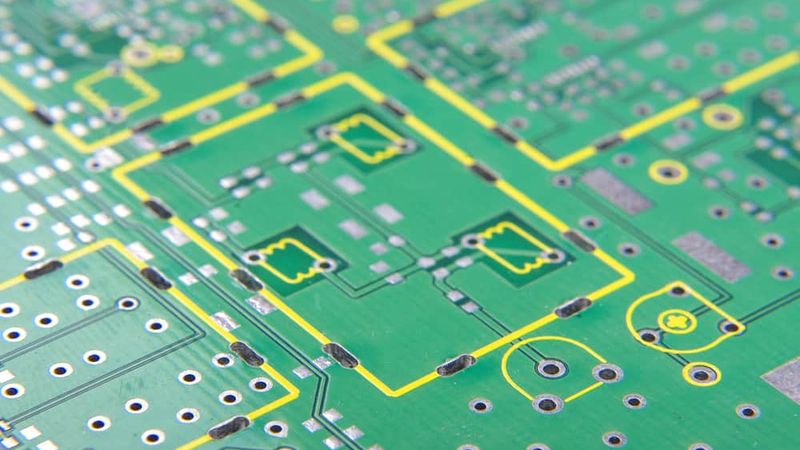
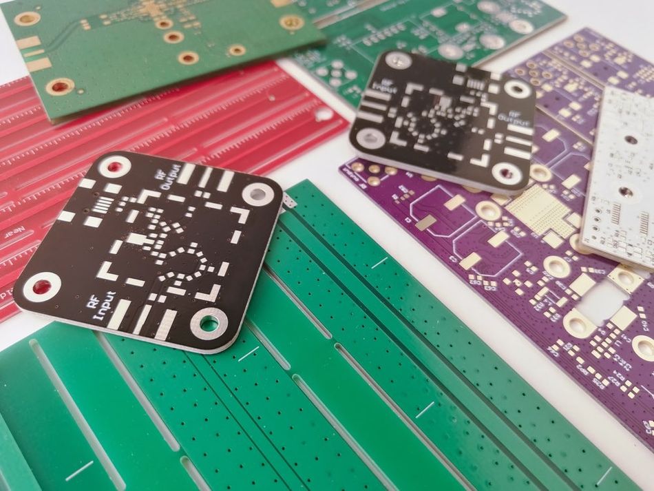
Silkscreen layer of a PCB in the view (green color)
No time now? Save for later.
We only use your email to send this link. Privacy Policy.
Introduction
PCB silkscreen is an integral part of circuit board design. It serves as a communicative layer in PCB fabrication, providing vital information to manufacturers, engineers, and service technicians who may need to test or service the board.
The silkscreen is one of the many layers in a PCB design, also known as the silk layer. So, it effectively presents information about the circuit and its components, and is used as a reference for circuit assembly and troubleshooting. This article will discuss the intricacies involved in the design, manufacturing, and use of PCB silkscreens.
Recommended Reading: How Do Circuit Boards Work: A Comprehensive Guide to the Heart of Electronics
What is a silkscreen on a PCB?
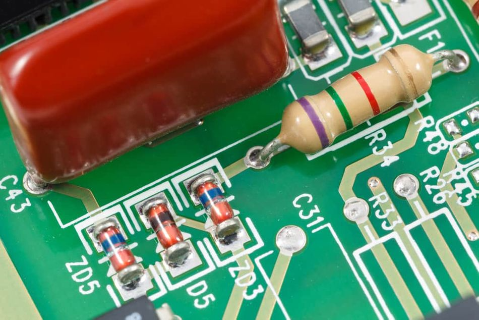
The silkscreen is a layer of ink traces that typically includes labels for the various components on the PCB, such as the names of the connectors and the values of resistors and capacitors. It may also include other information, such as the PCB's title, the polarity of parts, and the test point locations. The silkscreen is applied to the component part of the printed circuit board.
While it has many practical benefits, the silkscreen also serves a visual function, allowing manufacturers to add branding, company logos, and other decorative elements to the PCB, making the final product more attractive and professional-looking.
The ink used for the silkscreen layer is a non-conductive epoxy ink with several colours, including black, white, red, blue, and yellow.
What is the Role of PCB Silkscreen in Circuit Board Design
PCB silkscreen acts as a communicative layer, providing essential information to various stakeholders involved in the manufacturing, testing, and servicing of the board. This information typically includes component designators, test points, polarity marks, and other helpful assembly notes. Here are some critical roles that a silkscreen fulfils.
Assisting the Assembly Process
The silkscreen layer aids in the assembly process, guiding the placement of components on the PCB. It helps ensure that components are correctly and consistently placed, reducing the risk of errors during assembly. For instance, the silkscreen can indicate where a resistor should be placed and in what orientation, preventing potential mistakes that could affect the functionality of the board.
PCB Testing and Servicing
It helps in PCB testing and servicing. Test points marked on the silkscreen allow for easier debugging and repair. Service technicians can quickly identify components and understand their placement, making the troubleshooting process more efficient.
Impact on Manufacturing Process
The silkscreen also impacts the manufacturing process. The choice of silkscreen type and the precision of the application can affect the overall manufacturing time and cost. For example, using a Liquid Photo Imaging (LPI) process for silkscreen application can offer higher resolution and detail, but it may also increase the manufacturing time and cost compared to other methods like inkjet printing.
Types of PCB Silkscreen
In PCB manufacturing, there are primarily two types of silkscreen processes utilised:
- Liquid Photo Imaging (LPI)
- Direct Legend Printing (DLP)
Each of these methods has its unique characteristics, advantages, and disadvantages, and their application largely depends on the specific requirements of the PCB design.
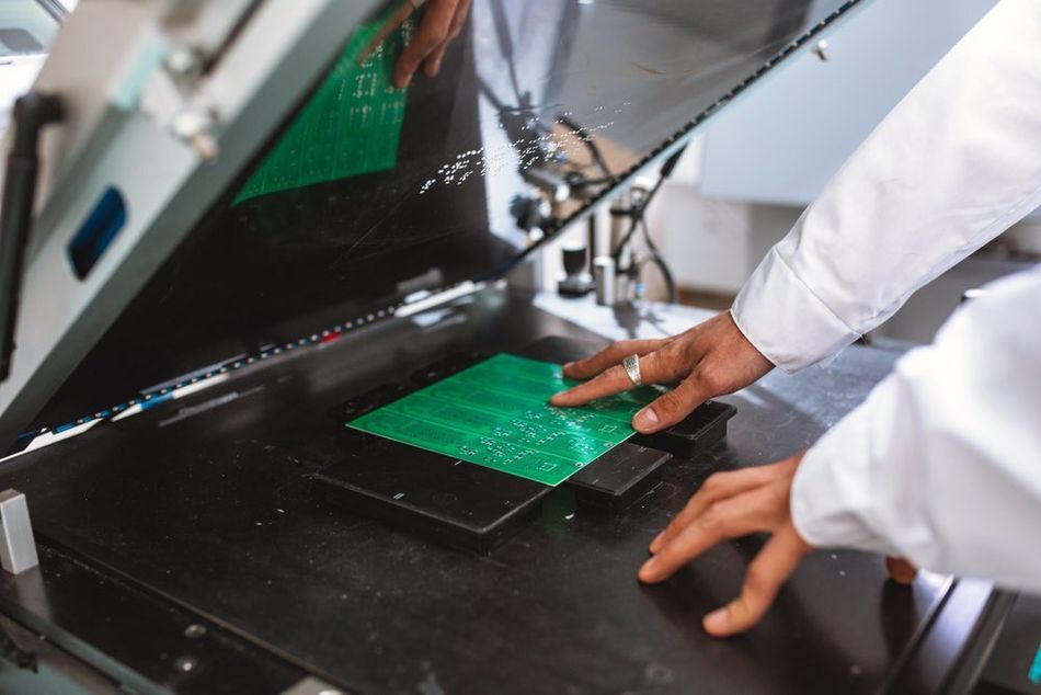
Liquid Photo Imaging (LPI)
Liquid Photo Imaging (LPI) is a widely used method for applying silkscreen on PCBs. A photosensitive liquid epoxy is applied onto the PCB, which is then exposed to ultraviolet light through a film that carries the desired legend pattern.
The UV exposure hardens the epoxy on the exposed areas, forming the legends on the PCB. The unexposed areas remain unhardened and are washed away in the developing process.
The LPI process is known for its high resolution and precision. It can produce fine lines and detailed legends, making it suitable for complex PCB designs that require a high level of detail on the silkscreen. The hardened epoxy also provides a protective layer over the printed legends, enhancing their durability and resistance to handling and environmental factors.
However, the process is more time-consuming and costly compared to other methods. The need for UV exposure and development adds to the manufacturing time, and the use of photosensitive epoxy and films increases the material costs. Furthermore, the LPI process requires specialised equipment and trained personnel, adding to the overall manufacturing cost.
Direct Legend Printing (DLP)
Unlike the LPI process, DLP uses inkjet technology to directly print the legends onto the PCB by using CAD software. The ink used in DLP is typically a specialized type that can adhere well to the PCB surface and withstand the subsequent manufacturing processes.
One of the main advantages of DLP is its speed and efficiency. Since it does not require any films or UV exposure, the DLP process can significantly reduce the manufacturing time. The direct printing also eliminates the need for any developing process, further speeding up the production.
In terms of quality, DLP can produce reasonably detailed legends, although it may not match the high resolution offered by the LPI process. However, for many standard PCB designs, the quality provided by DLP is more than sufficient.
DLP is more cost effective as it eliminates the use of films and photosensitive materials. Reduced the material costs, and faster production time also lead to to lower labour costs. Furthermore, the inkjet printers used in DLP are relatively simple and easy to operate, reducing the need for specialised training.
However, one potential drawback of DLP is the durability of the printed legends. The ink used in DLP may not be as resistant to handling and environmental factors as the hardened epoxy in the LPI process. Therefore, DLP may not be suitable for PCBs that require high durability of the silkscreen.
Manual Screen Printing
Manual screen printing is a method which uses a fine mesh screen to transfer the print onto the surface of a PCB. The process involves:
- Coating the screen with a layer of photosensitive emulsion
- Exposing it to light through a film positive of the design
- Washing away the emulsion to create a stencil of the design on the screen.
- Applying the ink to the screen, through the stencil onto the surface to be printed.
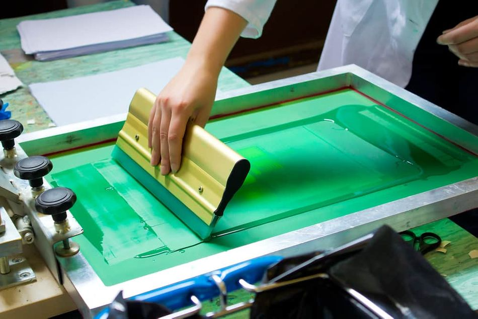
It’s a popular method for creating high-quality prints on various surfaces. It is often used for creating silkscreen on a PCB. Unlike automated printing methods, manual screen printing allows for more control over the printing process and can produce prints with finer detail and better resolution.
Different Methods to Create PCB Silkscreens
There are several methods for silkscreen printing on a PCB, including:
- Screen Printing: This is the most common method for creating the silkscreen on a PCB. It involves using a fine mesh screen to transfer the print onto the PCB.
- Inkjet Printing: This method uses an inkjet printer to print the silkscreen directly onto the PCB. The printer is equipped with a special printhead that can print on the surface of the PCB.
- Laser Printing: This method uses a laser to etch the silkscreen onto the PCB. The laser is guided by a computer-generated design, which burns away the PCB's surface to create the silkscreen
PCB Silkscreen Printing Process
The process of applying silkscreen to a PCB involves several steps, each of which plays a crucial role in ensuring the quality and accuracy of the final product. The general process can be broken down into three main stages:
- Preparing the silkscreen
- Applying the silkscreen
- Curing the silkscreen
Depending on the type of silkscreen printing method, there can be variations in each step, which is shown in the following table.
Silkscreen Printing Phase | What Is It? | LPI Process | DLP Process |
Silkscreen Preparation | It involves creating a stencil or mask that carries the desired legend pattern. The stencil can be made from various materials, such as polyester or stainless steel, depending on the silkscreen method used. | The stencil is a film that carries the negative of the legend pattern. It’s placed over the PCB, and the photosensitive epoxy is applied through the film. The areas of the film that are transparent allow the UV light to pass through and harden the epoxy, forming the legends on the PCB | The preparation involves programming the inkjet printer with the desired legend pattern. The printer uses this information to directly print the legends onto the PCB. |
Silkscreen Application | Applying the Silkscreen on to the PCB surface | Photosensitive epoxy is applied to the PCB through the stencil. The stencil is placed over the PCB, and the epoxy is spread over it. The areas of the stencil that are transparent allow the epoxy to pass through and adhere to the PCB. The stencil is then removed, leaving the epoxy on the PCB in the shape of the desired legends. | The inkjet printer directly prints the legends onto the PCB. The printer sprays the ink onto the PCB in the shape of the desired legends. The precision of the printer ensures that the legends are accurately printed on the PCB |
Silkscreen Curing | Curing involves hardening the silkscreen material, ensuring that it adheres properly to the PCB and remains durable throughout the board's lifecycle. The curing process varies depending on the type of silkscreen method used. | Curing involves exposing the PCB with the applied epoxy to ultraviolet (UV) light. The UV light hardens the epoxy, creating a durable and resistant layer on the PCB. The exposure time and intensity of the UV light must be carefully controlled to ensure proper curing. Insufficient exposure can result in a weak or brittle silkscreen, while overexposure can cause the epoxy to become too hard and prone to cracking. | the curing process typically involves thermal curing. The inkjet-printed legends are exposed to heat, which causes the ink to harden and adhere to the PCB surface. |
Considerations During the Silkscreen Printing
During each phase of silkscreen printing, manufacturers must ensure some essential considerations which include:
The thickness of the epoxy or ink, the pressure used in applying it, and the alignment of the stencil or printer all play a crucial role in the final result. Any errors or inconsistencies in these factors can lead to smudging, misalignment, or other defects in the silkscreen.
The temperature and duration of the thermal curing process must be carefully controlled to ensure optimal adhesion and durability of the silkscreen. Too low a temperature or insufficient curing time can result in a weak or easily damaged silkscreen, while excessive heat or prolonged curing can cause the ink to become brittle or discolored.
Further Reading: What are Circuit Boards Made Of? An Extensive Guide to Materials and Manufacturing Processes
Benefits of Using Silkscreen on a PCB?
There are several benefits to using silkscreen on a PCB, including:
Improved readability and clarity: The silkscreen provides labels and other information about the circuit and its components, which makes it easier to read and understand the PCB.
Easier assembly and troubleshooting: The silkscreen can be used as a reference for assembling and troubleshooting the circuit, saving time and effort.
Enhanced aesthetics: The silkscreen can be used to add branding, logos, and other decorative elements to the PCB, which can improve the appearance of the final product.
Improved durability: The silkscreen is applied on top of the other layers of the PCB, which means it is less likely to be damaged or worn away over time.
What are the Design Considerations for PCB Silkscreen?
Several factors must be considered to ensure the final product is functional, reliable, and easy to assemble, test, and service. Here is a quick look at the essential design considerations for PCB silkscreens.
Text Size and Placement
The size, and placement of text are the first critical parameter. The text must be legible and clearly visible to facilitate the assembly, testing, and servicing processes. To achieve this, designers should follow certain guidelines for optimal text size and placement such as:
The minimum recommended text size for PCB silkscreen is typically around 1 mm in height.Smaller text sizes may be difficult to read, while larger text sizes can take up valuable space on the PCB.Text should not interfere with the placement of components or soldering processes
Color and Contrast
The color of the silkscreen legends should provide sufficient contrast against the PCB substrate to ensure easy readability and identification of components, test points, and other relevant information.
The most common colour combination for PCB silkscreen is white text on a green or black substrate. This combination provides a high level of contrast, making the text easily visible and legible. However, other color combinations can also be used, depending on the specific requirements of the design and the preferences of the manufacturer or end-user.
When selecting colors for the silkscreen, it is essential to consider the manufacturing process and the materials used. Some colors may be more difficult to apply or may require additional processing steps, which can increase the manufacturing time and cost. Additionally, certain colors may be more susceptible to fading or discoloration over time, affecting the long-term readability of the silkscreen.
In addition to color, the contrast between the silkscreen legends and the PCB substrate is crucial for ensuring easy readability. High contrast between the text and the background makes it easier for technicians and engineers to identify components and other information on the PCB.
No Overlapping
While mentioning component symbols, names and other PCB details, they mustn’t overlap. So, the silkscreen must not overlap with other graphics on the board and PCB components like pads and vias. Ideally, it’s a good idea to keep at least a 5 mil gap between adjacent components to avoid silkscreen overlapping.
Conclusion
The PCB silkscreen is a critical component in the design and manufacturing of printed circuit boards. It provides essential information for both the assembly and troubleshooting processes, making it an indispensable tool for engineers and technicians. The choice of silkscreen type, whether it's Liquid Photo Imaging or Direct Legend Printing, depends on the specific requirements of the PCB, including the level of detail needed and the production budget. Design considerations such as text size, placement, color, and contrast also play a significant role in the effectiveness of the silkscreen. Lastly, quality control measures ensure the accuracy and durability of the silkscreen, contributing to the overall reliability of the PCB.
Frequently Asked Questions
What is a PCB silkscreen?
The PCB silkscreen is the layer on a printed circuit board where information like component designators, test points, logos, and warnings are printed.
What are the types of PCB silkscreen?
The two main types of PCB silkscreen are Liquid Photo Imaging (LPI) and Direct Legend Printing (DLP).
What is the role of the PCB silkscreen in circuit board design?
The PCB silkscreen provides essential information that guides the assembly process, aids in troubleshooting, and helps ensure the correct placement of components.
What are some design considerations for PCB silkscreen?
Design considerations for PCB silkscreen include the size and placement of text, as well as the color and contrast of the silkscreen against the PCB background.
How is quality control for PCB silkscreen maintained?
Quality control for PCB silkscreen involves checking the accuracy of the information printed, the clarity and legibility of the text, and the durability of the silkscreen under various conditions.
References
[1] 6 Must-Know Things About Silkscreen Printing of PCBs | Advanced Assembly
[2] Silk Screen Printing: What is it and How-To – Holden's Screen Supply
[3] PCB Silkscreen - Your Complete Guide - MorePCB
[4] PCB Silkscreen Guidelines | Blog | CircuitMaker (altium.com)
[5] T. Yan and M. D. F. Wong, "Recent research development in PCB layout," 2010 IEEE/ACM International Conference on Computer-Aided Design (ICCAD), 2010, pp. 398-403, doi: 10.1109/ICCAD.2010.5654190.
[6] A. Toprak and A. R. Boynuegri, "Printed Circuit Board Rapid Prototyping with Three-Dimensional Printer," 2020 4th International Symposium on Multidisciplinary Studies and Innovative Technologies (ISMSIT), 2020, pp. 1-7, doi: 10.1109/ISMSIT50672.2020.9254998.
[7] V. Anand, V. Singh and V. K. Ladwal, "Study on PCB Designing Problems and their Solutions," 2019 International Conference on Power Electronics, Control and Automation (ICPECA), 2019, pp. 1-5, doi: 10.1109/ICPECA47973.2019.8975402.
in this article
1. Introduction2. What is a silkscreen on a PCB?3. What is the Role of PCB Silkscreen in Circuit Board Design4. Types of PCB Silkscreen5. Different Methods to Create PCB Silkscreens6. PCB Silkscreen Printing Process7. Benefits of Using Silkscreen on a PCB?8. What are the Design Considerations for PCB Silkscreen?9. ReferencesNo time now? Save for later.
We only use your email to send this link. Privacy Policy.