Plasma Etching: A Comprehensive Guide to the Process and Applications
Understanding the Intricacies of Plasma Etching Systems, Mechanisms, Process types, Equipment and Applications of the Technology, its Impacts on the Environment, and Essential Safety Precautions for Safe and Productive Utilization of the Etching Technique.

14 Dec, 2023. 15 minutes read
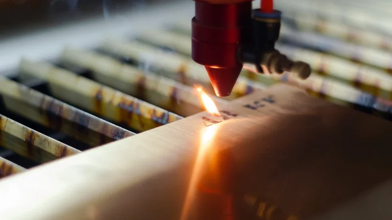
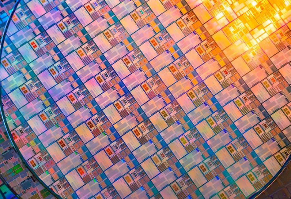
Plasma etching on a metallic surface
Introduction
Plasma etching is critical in various industries, particularly semiconductor manufacturing, microelectromechanical systems (MEMS), and nanotechnology. It’s a dry etching technique that leverages the unique properties of plasma to selectively remove material from a substrate, offering numerous advantages over traditional wet etching methods.
This article will delve into the fundamentals of plasma etching such as
Exploring the equipment and techniques
Discussing its applications across different industries
Addressing its environmental and safety considerations
Fundamentals of Plasma Etching
Plasma etching is a process used to remove material from the surface of a substrate using plasma. It uses highly energetic and reactive species produced from a selected process gas, such as O2, Argon, or a fluorine-bearing gas. These species are bombarded and reacted with the sample surface. It results in the breaking down of the material surface into volatile and smaller molecules. A vacuum system then removes these molecules.
The substrate, coated with the material to be etched and shielded by a patterned photoresist layer, sits on a temperature-controlled platen in the reactor. Reactive species from the plasma interact with the exposed material, producing a volatile byproduct expelled from the chamber. This controlled process allows engineers to precisely manage etching parameters, making plasma etching pivotal in diverse engineering domains, including semiconductor manufacturing and microelectromechanical systems (MEMS) fabrication.
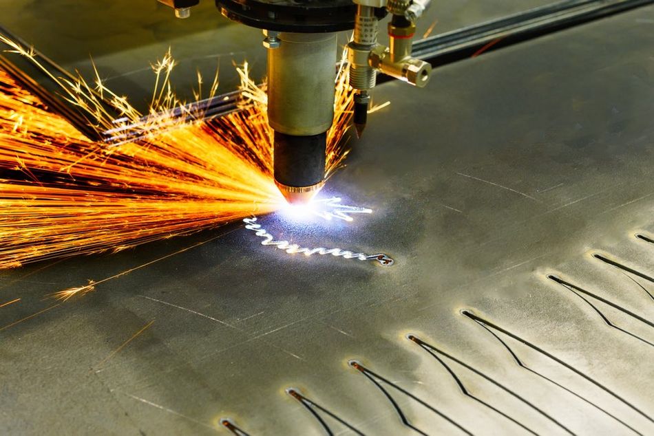 Fig 1: A plasma etching/cutting machine working on a metallic plate
What is Plasma?
Plasma is also referred to as the fourth state of matter. It’s an ionized gas consisting of free electrons, ions, and neutral particles. It is a highly energized state of matter where a significant portion of the atoms are ionized, meaning they have lost one or more electrons. This gives plasma unique properties distinct from other states such as:
- Free Electrons and Ions - Unlike solids, liquids, and gases, plasma contains a significant amount of free electrons and ions, making it electrically conductive. This characteristic is responsible for its diverse applications.
- High Energy - Plasma is a high-energy state of matter, with temperatures ranging from thousands to millions of degrees Celsius. This makes it highly reactive and capable of interacting with other materials in unique ways.
- Magnetically Confined - Due to its charged particles, plasma can be manipulated and confined using magnetic fields. This property is crucial for controlling plasma in various applications, such as fusion energy research.
- Luminosity - Because of the high energy, excited atoms in plasma emit light, giving it a characteristic glow or luminescence. This is why celestial bodies like stars and plasma lamps appear bright.
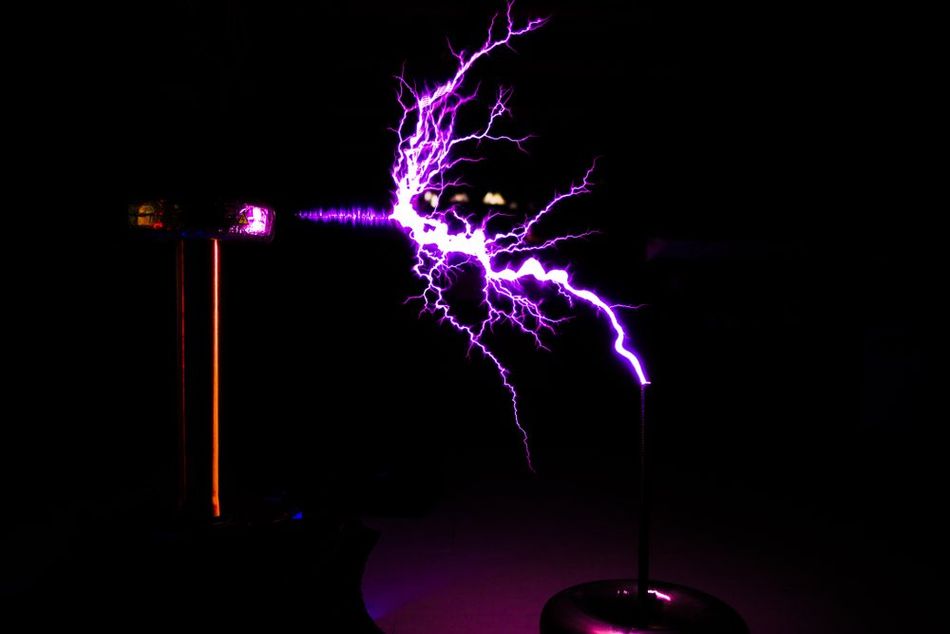 Fig 2: Tesla coil in operation with high energy lightning strikes
Some examples of plasma materials include lightning, neon signs, solar corona, fusion energy, and plasma TVs.
Types of Plasma
There are different types of plasma, including thermal (or equilibrium) and non-thermal (or non-equilibrium) plasma.
- Thermal plasma is characterized by similar temperatures of electrons and ions, typically in the range of thousands to tens of thousands of Kelvin.
- Non-thermal plasma has a significantly higher electron temperature than the ion temperature, allowing for efficient ionization at relatively low gas temperatures.
Plasma Etching Process
Etching is a process to selectively remove material from a substrate, typically to create patterns or structures in various applications, such as semiconductor manufacturing and MEMS fabrication.
There are two main types of etching i.e., wet etching and dry etching. Here is a quick look at these two mechanisms:
Wet Etching
Wet etching involves the use of liquid chemicals, known as etchants, to dissolve and remove material from the substrate. This process is typically isotropic, meaning that it etches in all directions equally, which can limit the precision and control of the etching process.
Dry Etching
Dry etching uses gases or plasmas to remove material from the substrate. Plasma etching is a form of dry etching that leverages the unique properties of plasma to achieve highly anisotropic etching. Hence, it allows for greater control and precision in the etching process. This is particularly important in applications where the creation of complex, high-resolution structures is required, such as in semiconductor manufacturing.
Why Plasma Etching is Better than Wet Etching?
Plasma etching offers several advantages over wet etching methods such as:
It provides better control over the etching process, enabling the creation of more precise and intricate structures.
It allows the use of a wider range of materials, as plasma etching can be tailored to target specific materials by adjusting the plasma chemistry.
It is a cleaner process, as it does not involve using hazardous liquid chemicals and generates less waste.
It’s easier to integrate into automated manufacturing processes, improving efficiency and reducing the potential for human error.
Further Reading: Dry Etching vs Wet Etching: A Comprehensive Comparison
Plasma Etching Mechanisms
Plasma etching operates through two primary mechanisms i.e., physical etching and chemical etching. The nature of the interactions between the plasma and the substrate material distinguishes these mechanisms.
Physical Etching
Physical etching, also known as sputtering or ion milling, involves the direct bombardment of the substrate by high-energy ions from the plasma. These ions collide with the atoms on the substrate surface, transferring their kinetic energy and causing the atoms to be ejected from the substrate.
- Physical etching is primarily anisotropic, meaning it etches in a single direction
- Anisotropic etching ensures the creation of sharp, well-defined features.,
- It can cause damage to the substrate due to the high-energy ion bombardment.
Chemical Etching
Chemical etching involves the reaction of reactive species from the plasma with the substrate material. These reactive species can be neutral or charged, They chemically react with the substrate atoms to form volatile compounds that can be easily removed from the substrate surface.
- Chemical etching is typically isotropic, meaning it etches in all directions equally
- It can be made anisotropic by using a plasma, which provides directional control over the reactive species.
Reactive Ion Etching (RIE)
In practice, most plasma etching processes involve a combination of both physical and chemical etching, known as Reactive Ion Etching (RIE). In RIE, the plasma generates reactive species for chemical etching, while the electric field in the plasma provides directional control for physical etching. This combination allows for the creation of complex, high-resolution structures with high aspect ratios.
Plasma Etching Equipment and Techniques
Plasma etching requires specialized equipment to generate and control the plasma, deliver the etching gases, and handle the substrate. The design and configuration of this equipment play a crucial role in determining the performance and capabilities of the plasma etching process.
Plasma Etching Systems
A typical plasma etcher system consists of several main components:
Plasma Generation Chamber
The plasma generation chamber is where the etching gases are ionized to form the plasma. It is typically made of materials that can withstand high temperatures and corrosive gases, such as quartz or stainless steel. The design of the chamber, including its size, shape, and electrode configuration, can significantly influence the properties of the plasma, which include:
- Density
- Uniformity
- Energy distribution
Gas Delivery System
The gas delivery system controls the flow of etching gases into the plasma chamber. This system usually includes:
- Gas supply lines
- Flow controllers
- Gas mixing chambers
The choice and mixture of gases determine the plasma chemistry, which in turn affects the etching rate, selectivity, and profile.
Substrate Holder
The substrate holder, also known as the wafer chuck, holds the substrate in place during the etching process. In addition to mechanical support, the substrate holder often provides thermal management to control the substrate temperature, which can influence the etching performance.
Vacuum System
The vacuum system maintains a low-pressure environment in the plasma chamber, which is necessary for plasma generation and control. This system typically includes a vacuum pump, pressure sensors, and control valves. The operating pressure affects the mean free path of the plasma particles, which can influence the etching directionality and uniformity.
Plasma Generation Technique
The generation of plasma is a critical step in the plasma etching process. There are several techniques for plasma generation, each with its advantages and limitations. These techniques can be broadly categorized into two types: direct and indirect plasma generation.
Direct Plasma Generation - An electric field is directly applied to a gas, which ionizes its atoms or molecules. This can be achieved through various methods, such as direct current (DC) discharge, radio frequency (RF) discharge, and microwave discharge.
DC Discharge - It uses a direct current between two electrodes, causing the gas to ionize and form a plasma. This method is simple and cost-effective, but it can lead to non-uniform plasma and electrode erosion due to the direct contact between the plasma and the electrodes.
RF discharge - It uses a high-frequency alternating current to ionize the gas. This method allows for better plasma uniformity and control than DC discharge, as the alternating current prevents charge buildup on the electrodes. However, RF discharge requires a more complex power supply and impedance-matching system.
Microwave Discharge - Uses high-frequency electromagnetic waves to ionize the gas. This method can generate high-density plasma with good uniformity, but it requires a waveguide or resonant cavity to confine and guide the microwaves, which can increase the complexity and cost of the system.
Indirect Plasma Generation - Requires the use of an external energy source to ionize the gas, such as electromagnetic fields or high temperatures. Examples of indirect plasma generation techniques include inductively coupled plasma (ICP) and helicon wave plasma.
Inductively Coupled Plasma (ICP) - ICP uses a high-frequency electromagnetic field, generated by an induction coil, to ionize the gas. This method can generate high-density, uniform plasma without direct contact between the plasma and the electrodes, reducing electrode erosion. But, they are more complex and expensive than direct plasma generation systems.
Further Reading: Ion Milling: A Comprehensive Guide to Material Etching Techniques
Process Parameters and Optimization
In plasma etching, several process parameters play a crucial role in determining the etching performance, including the etching rate, selectivity, and profile. These parameters can be carefully controlled and optimized to achieve the desired etching results.
Gas Flow Rate - The flow rate of the etching gases into the plasma chamber affects the concentration of reactive species and ions in the plasma. A higher gas flow rate can increase the etching rate but may also reduce the selectivity and uniformity of the etching process. Conversely, a lower gas flow rate can improve selectivity and uniformity but may result in a slower etching rate, which leads to the formation of a polymer layer on the substrate surface. A balanced gas flow rate is essential for achieving the desired etching performance.
Operating Pressure - The plasma chamber's operating pressure influences the plasma particles' mean free path, affecting the etching directionality and uniformity. Lower pressures result in longer mean free paths, promoting anisotropic etching and improving the etching profile. However, too low a pressure can reduce the plasma density and etching rate. On the other hand, higher pressures lead to shorter mean free paths, which can increase the etching rate but may result in less directional etching and poorer profile control.
Power - The power applied to the plasma generation system determines the energy and density of the plasma. Higher power levels can generate higher plasma densities, leading to faster etching rates. However, excessive power also causes high-energy ion bombardment that can damage the silicon wafer, and may also reduce the selectivity of the etching process. Optimizing the power level is crucial for balancing the etching rate, selectivity, and substrate integrity.
Temperature - The substrate and chamber temperature influence the etching performance. Higher temperatures can increase the etching rate by enhancing the chemical reactions between the reactive species and the substrate material. However, excessive temperatures can cause thermal stress and damage the substrate, reducing the etching process's selectivity.
Gas Chemistry - The choice and mixture of etching gases (etchant) determine the plasma chemistry, affecting the etching rate, selectivity, and profile. Different gases and gas mixtures can be used to tailor the plasma chemistry for specific materials and etching requirements. For example, fluorine-based gases are commonly used for etching silicon, while chlorine-based gases are used for etching metals such as aluminium and copper. Controlling the etchant levels can result in high selectivity for plasma etching.
Applications of Plasma Etching
Plasma etching is a versatile technique with various applications in various industries. Its ability to create precise, high-resolution features on various materials makes it a key process in many manufacturing and fabrication workflows.
Semiconductor Manufacturing
In the semiconductor industry, plasma etching is critical in fabricating integrated circuits (ICs). It is used to pattern the various layers of materials that make up an IC, including the semiconductor substrate, insulating layers, and metal interconnects.
IC fabrication involves a series of processes, including deposition, lithography, and etching, to create the complex, multi-layer structures that constitute the IC. In the etching step, a patterned mask is used to protect certain areas of the layer while the plasma etches away the exposed areas. This process is repeated for each layer of the IC, allowing for the creation of intricate structures with feature sizes down to the nanometer scale.
Plasma etching offers several advantages in IC fabrication such as:
- High etching rate and selectivity enable fast and precise patterning of the layers.
- The ability to etch in a single direction (anisotropic etching) allows for the creation of sharp, well-defined features, which is crucial for the miniaturization of ICs.
- Techniques like Pulsed Plasma Etching effectively eliminate unwanted micro-features like notching, micro-trenching, bowing, and aspect ratio-dependent etching.
Plasma etching is also vital in semiconductor manufacturing for forming vias and trenches in interconnect fabrication. Vias connect wiring layers through small holes, and trenches host wires by etching away the dielectric layer typically of silicon dioxide with a fluorocarbon-based plasma.
In addition to IC fabrication, plasma etching is also used in the manufacturing of other semiconductor devices, such as:
- Photovoltaic cells
- Complimentary Metal Oxide Semiconductor (CMOS) devices
- Llight-emitting diodes (LEDs).
In these applications, plasma etching creates various structures, such as microscale sensors and actuators in MEMS, p-n junctions in photovoltaic cells, and light-emitting layers in LEDs.
MEMS Manufacturing
Microelectromechanical systems (MEMS) are another significant area where plasma etching is extensively applied. MEMS are miniaturized devices that combine mechanical and electrical components, typically in the range of micrometres to millimetres.
In microelectronics fabrication, plasma etching is used to create microscale mechanical structures, such as cantilevers, bridges, and diaphragms, and electrical structures, such as capacitors and transistors.
These structures are used in various MEMS devices, including sensors, actuators, and microfluidic devices. For example, in a MEMS accelerometer, plasma etching is used to create a microscale mass and a set of capacitive plates, which can detect changes in acceleration based on the displacement of the mass and the resulting change in capacitance.
Nanotechnology Fabrication
Plasma etching is widely used in nanotechnology to fabricate nanoscale structures and devices, such as nanowires, quantum dots, and nano-electromechanical systems (NEMS). These nanoscale devices have unique properties and capabilities due to their small size and the quantum effects that come into play at the nanometer scale. For instance, in the fabrication of a quantum dot, plasma etching is used to create a tiny semiconductor particle that can confine electrons in a space small enough to exhibit quantum mechanical properties.
Biomedical Industry
In the biomedical industry, plasma etching fabricates medical devices and implants, lab-on-a-chip devices, and biosensors. For instance, small mesh tubes are used to treat narrow or weak arteries and plasma etching is employed to create intricate patterns and structures on the stent surface. This enhances the stent's mechanical properties and biocompatibility, improving its performance and patient outcomes.
Aerospace Industry
The aerospace industry also benefits from plasma etching, particularly in the manufacturing of microelectromechanical systems (MEMS) used in navigation and control systems. These MEMS devices, which include accelerometers and gyroscopes, rely on the precision and control offered by plasma etching to create their intricate, microscale structures. The high aspect ratio and anisotropic etching capabilities of plasma etching are particularly valuable in these applications.
Optical Industry
Plasma etching is used to fabricate optical components such as lenses, waveguides, and diffraction gratings. The process allows for creating high-precision, nanoscale features on these components, enabling the manipulation of light in ways that traditional optical components cannot achieve. For example, in the production of diffractive optical elements, plasma etching is used to create complex, sub-wavelength structures that can diffract and focus light in specific ways.
Further Reading: Understanding Plasma Etching: Detailed Insights into Its Techniques, Uses, and Equipment Maintenance
Environmental and Safety Considerations
Plasma etching, like many industrial processes, has environmental and safety considerations that must be addressed. These include the handling and disposal of etching gases, the generation of waste products, and the safety of the operating personnel.
Environmental Impact
The environmental impact of plasma etching primarily stems from the etching gases used in the process. Here are some critical aspects of its ecological impact:
Global Warming - Many of these gases are greenhouse gases, which contribute to global warming when released into the atmosphere. For example, sulfur hexafluoride (SF6) and perfluorocarbons (PFCs), which are commonly used in plasma etching, have global warming potentials several thousand times higher than carbon dioxide.
Ozone Layer Depletion - Some etching gases are also harmful to the ozone layer as Chlorofluorocarbons (CFCs), once widely used in plasma etching, are known to deplete the ozone layer and have been largely phased out due to international regulations.
Toxic Materials - In the photovoltaic industry, plasma etching involves the use of highly toxic, corrosive, and flammable materials like chlorides, bromides, and fluorides. These materials pose a threat not only to the environment but also to human lives.
To mitigate these environmental impacts, various strategies can be employed. These include using less harmful etching gases, recycling or reclamation of spent gases, and treating waste products to render them less harmful. Additionally, process optimization can reduce the amount of etching gases used and waste generated, further reducing the environmental impact of the process.
Safety Precautions
Safety is a paramount concern in plasma etching operations. The use of high-energy plasma, hazardous gases, and potentially toxic etched materials, poses risks to operating personnel and require appropriate safety measures.
Handling - Many of these gases are toxic, corrosive, or reactive, and can cause harm if inhaled, come into contact with skin, or react with other substances.
Personal Protective Equipment - Etching gases should be properly stored and appropriate personal protective equipment (PPE), such as gloves, safety glasses, and respirators, should be used.
Detection Systems - The plasma etching system should be equipped with gas detection and alarm systems to alert operators in case of a gas leak.
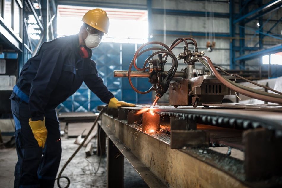 Fig 5: A worker wearing the essential PPEs while working with a plasma cutter
The high-energy plasma used in the etching process also poses safety risks. The plasma can generate ultraviolet (UV) radiation, which can cause eye and skin injuries. To protect against this, the plasma chamber should be shielded to block UV radiation, and operators should wear UV-protective eyewear. The plasma can also generate electromagnetic fields, which can interfere with electronic devices and potentially cause harm to individuals with pacemakers or other electronic medical devices.
Conclusion
Plasma etching is a critical process in various industries, from semiconductor manufacturing to biomedical applications. Its ability to create precise, high-resolution features on a wide range of materials makes it a versatile and valuable tool in many manufacturing and fabrication processes. However, the process also has environmental and safety considerations that must be addressed, including the handling and disposal of etching gases, the generation of waste products, and the safety of the operating personnel. By understanding these aspects and implementing appropriate measures, the benefits of plasma etching can be fully realized while minimizing its potential risks and impacts.
Frequently Asked Questions (FAQs)
What is plasma etching?
Plasma etching is used in various industries to create precise, high-resolution features on various materials. It involves using high-energy plasma and etching gases to remove material from a substrate selectively.
What are the applications of plasma etching?
Plasma etching is used in various applications, including the fabrication of integrated circuits in the semiconductor industry, the creation of microscale and nanoscale structures in MEMS and nanotechnology, and the manufacturing of devices in the biomedical, aerospace, and optical industries.
What are the environmental impacts of plasma etching?
The environmental impacts of plasma etching primarily stem from the etching gases used in the process, many of which are greenhouse gases. The process also generates waste products, which can be hazardous and require proper disposal.
What safety precautions are needed in plasma etching?
Safety precautions in plasma etching include the proper storage and handling of etching gases, the use of personal protective equipment, the shielding of the plasma chamber to block UV radiation and electromagnetic fields, and the proper collection and disposal of etched materials. Regular maintenance and inspection of the plasma etching system, proper training of operating personnel, and adherence to safety regulations are also important.
How can the environmental impact of plasma etching be reduced?
The environmental impact of plasma etching can be reduced by using less harmful etching gases, recycling or reclaiming spent gases, treating waste products to render them less harmful, and optimizing the process to reduce the amount of etching gases used and waste generated.
References
[1] J.H. Wang. (2012), “Coatings for Biomedical Applications” https://www.sciencedirect.com/topics/materials-science/plasma-etching
[2] Gomathi Nageswaran, Saravanakumar Jagannathan. (2019), “Non-Thermal Plasma Technology for Polymeric Materials”
https://www.sciencedirect.com/topics/materials-science/ion-implantation
[3] Zai-fa Zhou; Qing-an Huang; Wei-hua Li; Chi Zhu. (2006). “Plasma Etching Process Simulation for MEMS and IC Fabrication based on a Cellular Automata Method”
https://ieeexplore.ieee.org/document/4098429
[4] Demetre J Economou. (2014), “Pulsed plasma etching for semiconductor Manufacturing” Topical Review (uh.edu)
[5] T Chiad, Bahaa & Al-zubaydi, Thair & Khalaf, Mohammed & Khudiar, Ausama. (2010). Characterization of low pressure plasma-dc glow discharges (Ar, SF6 and SF6/He) for Si etching. Indian Journal of Pure and Applied Physics. 48. 723-730.
[6] Difference Between Isotropic And Anisotropic - Differences explained on BYJU’S (byjus.com)
in this article
1. Introduction2. Fundamentals of Plasma Etching3. Fig 1: A plasma etching/cutting machine working on a metallic plate4. Plasma Etching Process5. Plasma Etching Mechanisms6. Plasma Etching Equipment and Techniques7. Applications of Plasma Etching8. Environmental and Safety Considerations9. Conclusion10. Frequently Asked Questions (FAQs)11. References