Rigid PCB: Complete Engineering Guide & Advanced Design Techniques 2025
Understanding the need for Rigid PCB technology, capturing its manufacturing process and applications, and the innovations it has brought in modern electronics design and industrial manufacturing.

Last updated on 25 Jun, 2025. 12 minutes read
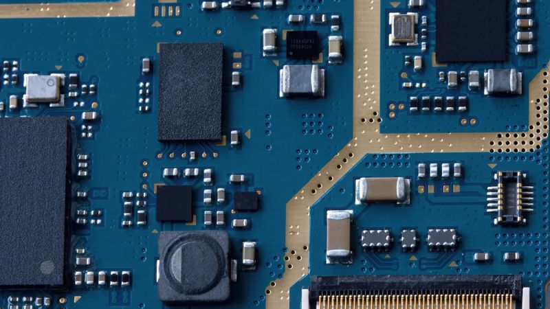
Rigid PCB are integral part of modern consumer electronics
Introduction
In the world of modern electronics, the Printed Circuit Board (PCB) serves as the foundational backbone, connecting disparate components into a cohesive, functional system. Among the various types, rigid PCBs remain paramount due to their durability, reliability, and widespread applicability across industries, from consumer gadgets to aerospace and medical devices.
This article delves into the evolving landscape of rigid PCB design, exploring advanced techniques that push the boundaries of performance and miniaturization, the critical role of seamless integration, and the sophisticated software tools that empower engineers to navigate these complexities and bring cutting-edge electronic innovations to life.
Theoretical Foundations Reveal Rigid PCB's Structural Engineering Principles
Modern rigid PCB technology achieves 99.9% dimensional stability through sophisticated substrate engineering and multi-layer lamination processes. A rigid printed circuit board represents a non-flexible electronic interconnection platform built upon a solid substrate material that provides mechanical support and electrical insulation for electronic components.
The fundamental physics underlying rigid PCB performance centers on the glass transition temperature (Tg) of the substrate material, typically 130-180°C for standard FR4, which determines thermal stability and operational reliability.
The mechanical properties of rigid PCBs derive from their composite structure, combining woven fiberglass reinforcement with epoxy resin matrices. Standard FR4 substrate exhibits tensile strength of 310 MPa and flexural strength of 415 MPa, providing exceptional durability for demanding applications.
Suggested Reading: FR4: Understanding the Material and Its Applications in PCB Design
The dielectric constant of FR4 ranges from 4.2-4.6 at 1 MHz, directly impacting signal propagation velocity according to the relationship:
v = c / √(εr × μr)
Where v represents signal velocity, c is the speed of light, εr is relative permittivity, and μr is relative permeability. This fundamental equation governs high-speed signal integrity calculations that are essential for modern digital systems operating above 100 MHz.
The rigid PCB architecture enables component density improvements of 300-500% compared to traditional wire-wrap techniques. It also ensures superior electromagnetic compatibility through controlled impedance design. Multilayer rigid PCBs can achieve up to 40 layers in advanced applications, with each additional layer increasing routing density by approximately 15-20%.
Recommended Reading: What is a Multilayer PCB?
Advanced Design Techniques Leverage Electromagnetic Field Analysis
High-density interconnect (HDI) design methodologies revolutionize rigid PCB capability through microvias with diameters as small as 0.1mm and trace widths approaching 25 micrometers. The implementation of HDI technology in 2025 enables component density increases exceeding 400% while maintaining signal integrity through advanced electromagnetic field modeling.

Signal integrity analysis requires precise calculation of characteristic impedance using the following relationship for microstrip transmission lines:
Z₀ = (87/√(εr+1.41)) × ln(5.98h/(0.8w+t))
Where h represents substrate height, w is trace width, t is copper thickness, and εr is dielectric constant. Modern rigid PCB designs target impedance tolerances within ±5% to ensure optimal signal transmission.
The design process for 2025 rigid PCB projects follows these critical steps:
Stackup optimization - Determine layer count based on signal routing requirements and power distribution needs.
Component placement - Utilize AI-driven placement algorithms, achieving 35% routing efficiency improvements.
Thermal analysis - Implement copper planes providing thermal conductivity of 385 W/m·K for heat dissipation.
EMI mitigation - Design guard traces and via fencing, reducing electromagnetic interference by 25-40 dB.
Automated design rule checking (DRC) in modern CAD tools identifies 95% of potential manufacturing issues before fabrication, significantly reducing prototype iteration cycles. The integration of machine learning algorithms in PCB routing optimization demonstrates timing closure improvements of 40-60% for complex digital designs.
Recommended Reading: How Advanced Circuit Boards Enhance Device Functionality
Common Applications of Rigig PCBs
Automotive Systems Manufacturing
The automotive electronics sector represents the fastest-growing rigid PCB market segment, expanding at 8.2% CAGR through 2028. Electric vehicle applications demand rigid PCBs capable of operating across temperature ranges from -40°C to 125°C while maintaining functional reliability for 150,000+ thermal cycles. Tesla's Model S utilizes over 60 rigid PCBs throughout its electronic control systems, demonstrating the critical role of these components in modern automotive design.
Aerospace Systems
Aerospace and defense applications leverage rigid PCBs operating in extreme environments with radiation tolerance up to 100 krad and vibration resistance meeting MIL-STD-810G standards. For instance, Boeing 787 aircraft incorporate over 2,000 rigid PCBs across avionics, flight control, and passenger entertainment systems. The aerospace sector requires thermal cycling from -55°C to 125°C for 2,000+ cycles without performance degradation.
5G Communication Systems
5G infrastructure deployment drives demand for rigid PCBs supporting frequencies up to 28 GHz, requiring specialized low-loss dielectric materials with dissipation factors below 0.002. The telecommunications industry projects rigid PCB volume growth of 12% annually through 2027 as network densification accelerates.
Medical Device Manufacturing
Medical device applications require rigid PCBs meeting IPC-6012DA Class 3 standards with enhanced reliability specifications. Pacemaker control circuits utilize rigid PCBs with MTBF ratings exceeding 20 years, achieved through component derating and hermetic packaging. The medical electronics market demands leakage currents below 10 microamperes to ensure patient safety, necessitating specialized substrate materials and manufacturing processes.
Industry Sector | Operating Temperature | Reliability Requirement | Market Value (2025) |
Automotive | -40°C to 125°C | 150K thermal cycles | |
Medical | 0°C to 70°C | 20+ year MTBF | |
Aerospace | -55°C to 125°C | MIL-STD compliance | |
Consumer | -10°C to 85°C | 10K power cycles |
Integration With Flexible Circuits Enables Revolutionary Form Factors
Rigid-flex PCB technology combines the mechanical stability of rigid boards with the dynamic flexibility of polyimide circuits, enabling 3D packaging solutions that reduce overall product volume by 40-60%. The manufacturing process utilizes no-flow prepregs costing $1.50-3.00 per square foot compared to $0.25 per square foot for standard prepregs, resulting in 7x higher costs than traditional rigid boards.
Bending radius calculations for flexible sections follow the relationship R ≥ 6t, where R represents the minimum bend radius and t is the total flexible stack thickness. Dynamic flexing applications require bend radii exceeding 10 times the flexible thickness to achieve 1 million+ flex cycles without failure. The integration of rigid and flexible sections demands precise impedance matching within ±10% across transition zones.
Suggested Reading: Understanding PCB Thickness: A Comprehensive Guide
Common integration challenges include:
Impedance discontinuities at rigid-flex boundaries cause signal reflections exceeding -20 dB
There is a likelihood of thermal expansion mismatch between FR4 (17 ppm/°C) and polyimide (20 ppm/°C) substrates
Via reliability concerns are persistent in high-stress transition areas, requiring enhanced plating thickness of 35+ micrometers.
Recommended Reading: Why Should You Use Rigid-Flex PCB Assembly?
Modern Software Tools Revolutionize PCB Design Implementation
Altium Designer
Altium 2025 dominates the professional PCB design market with unified design environments supporting up to 40-layer stackups and integrated 3D mechanical collaboration. The latest version incorporates AI-powered component placement algorithms reducing design time by 35% while maintaining optimal thermal and electrical performance.
KiCad
KiCad (Open Source Community, 2025) provides comprehensive PCB design capabilities with advanced 3D visualization and SPICE simulation integration at zero licensing cost. The platform supports multilayer designs up to 32 layers with professional-grade design rule checking and gerber export capabilities.
Software Tool | Developer | Key Strengths | Cost Model | Market Share |
Altium Designer | Altium | AI placement, 3D integration | $7,245/year | |
KiCad | Open Source | Free, extensible, cross-platform | Free | |
Eagle | Autodesk | Fusion 360 integration | $500/year | |
OrCAD | Cadence | Simulation, signal integrity | $3,000+/year | |
PADS | Siemens | Thermal analysis, DFM | $4,500/year |
Advanced simulation capabilities in 2025 tools include electromagnetic field solving with convergence times under 30 minutes for complex 20+ layer designs. Thermal simulation accuracy improves to within ±3°C of measured values through enhanced material modeling and boundary condition handling.
Design for Manufacturing (DFM) checking algorithms identify 98% of potential fabrication issues during the design phase, including minimum trace width violations, via aspect ratio problems, and solder mask clearance errors. Automated optical inspection (AOI) integration provides real-time feedback with manufacturing partners, reducing prototype turnaround times from 10-14 days to 5-7 days.
Best Practices Address Common Implementation Pitfalls
Via aspect ratio limitations represent the most frequent rigid PCB failure mode, with ratios exceeding 12:1 causing plating reliability issues in standard manufacturing processes. HDI technology enables via aspect ratios up to 6:1 through laser drilling, providing superior reliability for high-density applications.
Critical design guidelines for 2025 rigid PCB implementations include:
Minimum trace width specification - Maintain 100 micrometer traces for standard manufacturing and 50 micrometer traces for HDI processes.
Copper balance requirements - Achieve ±30% copper balance across all layers to prevent board warpage during reflow.
Thermal via implementation - Use thermal vias with 0.2mm diameter at 0.5mm spacing for components dissipating more than 1W power.
Signal layer adjacency - Separate high-speed signals from switching power planes by a minimum of 200 micrometers
Component orientation standardization - Align all polarized components in consistent directions, reducing assembly errors by 60%.
Adherence with IPC Class 2 Standards
IPC-6012DA Class 2 standards specify maximum conductor resistance of 20% above calculated values, ensuring consistent electrical performance across production volumes. Environmental testing per IPC-TM-650 requires 500+ thermal cycles from -40°C to 125°C without degradation.
Suggested Reading: IPC Standards: The Definitive Guide for Electronics Engineers and PCB Designers
Soldermask Tolerance and Silkscreen Legibility
Solder mask registration tolerances of ±75 micrometers prevent solder mask-defined pad issues that cause assembly defects. Silkscreen legibility requires minimum 0.15mm line widths and 1.0mm character heights for automated optical inspection compatibility .
Suggested Reading: PCB Solder Mask: Everything You Need to Know
RoHS Compliance
RoHS compliance mandates lead-free solder processes operating at 245-260°C, requiring substrate materials with glass transition temperatures exceeding 170°C. Halogen-free FR4 alternatives provide environmental compliance while maintaining electrical and mechanical performance specifications.
Recent Developments in Rigid PCB Design
Quantum Computing
Quantum computing applications introduce unprecedented rigid PCB design challenges, requiring cryogenic operation at 4 Kelvin with specialized low-temperature dielectric materials. For example, IBM's 433-qubit Osprey processor utilizes custom rigid PCBs with superconducting interconnects, demonstrating the frontier of PCB technology applications.
Suggested Reading: The Role Of Quantum Computing In Manufacturing
Environmental Sustainability
Environmental sustainability initiatives drive adoption of bio-based PCB substrates, with recyclable content exceeding 70% in next-generation materials. Halogen-free flame retardants replace traditional bromine-based additives, reducing environmental impact while maintaining UL94 V-0 flammability ratings.
Further Reading: The Building Blocks of Innovation: Inks, Substrates, and Solder Pastes for Additive PCBs and Flexible Electronics
Industry 4.0
Industry 4.0 manufacturing integration enables real-time PCB quality monitoring with automated optical inspection, achieving 99.8% defect detection accuracy. Smart factory implementations reduce PCB manufacturing lead times from 10 days to 3 days through optimized production scheduling and automated material handling.
Recommended Reading: Smart Factory: When Digitization Meets Connectivity
Advanced Techniques Reveal Sophisticated Applications
Embedded Components
Embedded component technology integrates passive elements within PCB substrate layers, achieving 30-50% size reduction in high-density applications. Capacitor embedding utilizes specialized dielectric layers with permittivity values exceeding 1000, enabling microfarad-level capacitance in minimal board area..
3D PCB Printing
3D PCB printing technology emerges as a disruptive manufacturing approach, enabling conformal circuit geometries impossible with traditional fabrication. Nano Dimension's DragonFly systems print conductive silver inks with 10-micrometer resolution, opening new possibilities for prototype development and low-volume production.
Optical Interconnects
Optical interconnect integration combines rigid PCBs with embedded waveguides, supporting data rates exceeding 100 Gbps per channel for high-performance computing applications. Silicon photonics integration requires specialized PCB substrates with thermal expansion coefficients matching silicon (2.6 ppm/°C).
Quantitative Performance Metrics Guide Engineering Decisions
Thermal resistance calculations determine component reliability using the relationship:
θJA = (TJ - TA) / P
where θJA represents junction-to-ambient thermal resistance, TJ is junction temperature, TA is ambient temperature, and P is power dissipation.
Standard FR4 PCBs achieve thermal resistance of 40-60°C/W per square inch without additional thermal management.
Signal integrity metrics require rise time calculations using tr = 2.2 × √(L × C), where L represents inductance and C represents capacitance per unit length.
High-speed digital signals with 100 ps rise times demand trace lengths under 15mm without proper termination.
Here is the cost-benefit analysis for HDI versus standard rigid PCB technology:
Metric | Standard PCB | HDI PCB | Performance Gain |
Component Density | 100% baseline | 400% | 4x improvement |
Layer Count | 8 layers max | 20+ layers | 2.5x capacity |
Manufacturing Cost | $2.50/sq in | $8.00/sq in | 3.2x cost increase |
Assembly Yield | 98% | 94% | 4% yield reduction |
Signal Integrity | 80% margin | 95% margin | 15% improvement |
Conclusion
The rigid PCB industry is at a pivotal point, blending significant technological leaps with a strong commitment to environmental stewardship. By 2030, we expect AI-powered design tools to automate 90% of layout tasks, while quantum computing will push material science to new frontiers. Alongside these advancements, sustainable manufacturing initiatives aim to cut environmental impact by 50%, fundamentally changing production through bio-based materials and circular economy principles.
With the market projected to reach $117.53 billion by 2032, rigid PCBs are central to the development of 5G networks, electric vehicles, and IoT ecosystems. Engineers in this field must therefore master advanced simulation tools, grasp quantum-scale electromagnetic effects, and adopt sustainable design practices. The coming decade of rigid PCB innovation will be defined by the convergence of artificial intelligence, quantum computing, and environmental responsibility, offering exciting opportunities for those ready to embrace these transformative changes.
Frequently Asked Questions
What is the difference between rigid and flexible PCBs?
Rigid PCBs use solid substrate materials like FR4 fiberglass that cannot bend, while flexible PCBs use polyimide materials, allowing dynamic flexing. Rigid boards provide superior mechanical support and cost 70% less than flexible alternatives.
How many layers can a rigid PCB support?
Modern rigid PCBs support up to 40 layers in advanced applications, with 8-12 layers typical for consumer electronics. Each additional layer increases routing density by 15-20% while adding $2-4 per square inch to manufacturing cost.
What temperature range do rigid PCBs operate in?
Standard FR4 rigid PCBs operate from -40°C to 125°C, with high-temperature variants reaching 200°C. Automotive applications require extended temperature operation with 150,000+ thermal cycles.
How do you calculate rigid PCB manufacturing cost?
PCB cost = (Area × Layer Count × $0.35-0.45) + Setup Fees, with typical costs ranging $2-8 per square inch depending on complexity. HDI designs cost 3-4x more than standard fabrication.
What are the key design rules for rigid PCB layout?
Critical rules include a minimum 100-micrometer trace width, 12:1 maximum via aspect ratio, ±30% copper balance, and 200-micrometer separation between signal and power planes. IPC-6012DA standards specify detailed requirements.
How long does rigid PCB manufacturing take?
Standard rigid PCB fabrication requires 5-10 days, with HDI designs taking 10-15 days. Prototype services offer a 24-48 hour turnaround for simple designs under 6 layers.
What software is best for rigid PCB design?
Altium Designer leads professional applications with 35% market share, while KiCad provides excellent open-source capabilities. Tool selection depends on budget, complexity requirements, and team collaboration needs.
References
PCBElec, "Rigid PCB Circuit Board - Definition, Types, and Applications," PCB Electronics, 2023. [Online]. Available: https://www.pcbelec.com/pcb-manufacturing/rigid-pcb
PCB Directory, "What is a Rigid PCB?" PCB Directory, Jan. 15, 2025. [Online]. Available: https://www.pcbdirectory.com/community/what-is-a-rigid-pcb
Würth Elektronik, "RIGID.flex PCB solutions," 2021. [Online]. Available: https://www.we-online.com/en/products/printed-circuit-boards/flex-solutions/rigid-flex
MCL, "Rigid vs. Flexible PCBs: How to Choose Your PCB Type," Oct. 12, 2021. [Online]. Available: https://www.mclpcb.com/blog/rigid-vs-flexible/
Altium, "The Rigid-Flex PCB Manufacturing and Fabrication Process," Oct. 1, 2024. [Online]. Available: https://resources.altium.com/p/rigid-flex-pcb-fabrication-process
Fineline Global, "Rigid-Flex PCBs," Nov. 9, 2022. [Online]. Available: https://www.fineline-global.com/knowledge-centre/rigid-flex-pcbs/
Fastlink Electronics, "Applications and Advantages of Rigid PCBs," [Online]. Available: https://www.fastlink-electronics.com/applications-and-advantages-of-rigid-pcbs/
PCBMake, "Comprehensive Analysis of FR4 Substrate Data Sheet," Jun. 16, 2024. [Online]. Available: https://pcbmake.com/fr4-substrate-datasheet/
Andwin Circuits, "Rigid flex pcb fabrication process," Aug. 3, 2024. [Online]. Available: https://www.andwinpcb.com/rigid-flex-pcb-fabrication-process-2/
Zuken, "PCB Stack-up Design Rules," May 14, 2023. [Online]. Available: https://www.zuken.com/us/blog/pcb-stack-up-design-rules/
All Flex Solutions, "Rigid Flex PCB Cost Comparison: Here's What You Need to Know," Mar. 21, 2025. [Online]. Available: https://www.allflexinc.com/blog/rigid-flex-pcb-cost-comparison/
Rocket PCB, "Analysis of the current status and future development prospects of the PCB industry market in 2025," Apr. 15, 2025. [Online]. Available: https://www.rocket-pcb.com/analysis-of-the-current-status-and-future-development-prospects-of-the-pcb-industry-market-in-2026
Zetwerk, "Top Trends in PCB Manufacturing for 2025 and Beyond," Jan. 1, 2025. [Online]. Available: https://www.zetwerk.com/resources/knowledge-base/electronics-manufacturing-services-ems/top-trends-in-pcb-manufacturing-for-2025-and-beyond/
Zuken, "The Top PCB Design Trends to Watch in 2025," Mar. 17, 2025. [Online]. Available: https://www.zuken.com/en/blog/the-top-pcb-design-trends-to-watch-in-2025/
BesterPCBA, "What is Mean Time Between Failure (MTBF)," Jan. 2, 2024. [Online]. Available: https://www.besterpcba.com/what-is-mean-time-between-failure-mtbf/
FCPCBA, "RoHS Compliance Standard: RoHS-compliant PCB Assembly," Mar. 19, 2025. [Online]. Available: https://www.fcpcba.com/wiki/rohs-compliance-for-pcb/
CopperDot, "HDI PCBs — high-density interconnect printed circuit boards," [Online]. Available: https://www.copperdot.ai/portfolio/hdi-pcb/
Midwest PCB, "How AI and Machine Learning Are Revolutionizing PCB Design," Mar. 24, 2025. [Online]. Available: https://www.midwestpcb.com/how-ai-and-machine-learning-are-revolutionizing-pcb-design/
ALLPCB, "Top 10 PCB Design Software Tools for Engineers in 2025," Jan. 1, 2023. [Online]. Available: https://www.allpcb.com/blog/pcb-design/top-10-pcb-design-software-tools.html
FS PCBA, "Top 5 PCB Design Software Comparison in 2024: Which Is Best for You?," Dec. 5, 2024. [Online]. Available: https://www.fs-pcba.com/pcb-cad-softwares/
KiCad EDA, "KiCad EDA - Schematic Capture & PCB Design Software," May 7, 2025. [Online]. Available: https://www.kicad.org
IPC, "Electrical Test Conditions & Consideration," [Online]. Available: https://www.ipc.org/system/files/technical_resource/E2&S26_01.pdf
Tessolve, "Designing 5G PCBs: Key Considerations for Connectivity," May 2, 2025. [Online]. Available: https://www.tessolve.com/blogs/designing-for-5g-pcb-considerations-for-next-generation-connectivity/
911EDA, "Quantum PCB Design: Adapting to New Tech Challenges," Jul. 9, 2024. [Online]. Available: https://www.911eda.com/articles/quantum-pcb-design-adapting-to-new-tech-challenges/
Plain Concepts, "Quantum Computing: What are its challenges and potential," Oct. 7, 2024. [Online]. Available: https://www.plainconcepts.com/quantum-computing-potential-challenges/
Gatema PCB, "Printed Circuit Boards for the Automotive Industry," Feb. 6, 2025. [Online]. Available: https://www.gatemapcb.com/printed-circuit-boards-for-the-automotive-industry/
RayPCB, "Top 15 PCB Requirements in medical devices," Nov. 17, 2023. [Online]. Available: https://www.raypcb.com/pcb-requirements-in-medical-devices/
Andwin PCB, "Green PCB Manufacturing: Sustainable Practices for the Electronics Industry," Apr. 30, 2025. [Online]. Available: https://www.andwinpcb.com/green-pcb-manufacturing-sustainable-practices-for-the-electronics-industry/
in this article
1. Introduction2. Theoretical Foundations Reveal Rigid PCB's Structural Engineering Principles3. Advanced Design Techniques Leverage Electromagnetic Field Analysis4. Common Applications of Rigig PCBs5. Integration With Flexible Circuits Enables Revolutionary Form Factors6. Modern Software Tools Revolutionize PCB Design Implementation7. Best Practices Address Common Implementation Pitfalls8. Recent Developments in Rigid PCB Design 9. Advanced Techniques Reveal Sophisticated Applications10. Quantitative Performance Metrics Guide Engineering Decisions11. Conclusion12. Frequently Asked Questions13. References