Tapeout in Semiconductor Manufacturing: An In-depth Exploration
Unveiling the Evolution, History, and Significance of the Tapeout Process in Semiconductor Manufacturing.

19 Jan, 2024. 12 minutes read
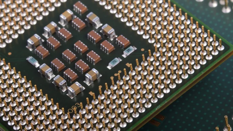
A semiconductor chip designed via tapeout
What is Tapeout in Semiconductor Manufacturing?
In the context of semiconductor manufacturing, Tapeout is a significant milestone in the production of integrated circuits (ICs). The term originates from the era of reel-to-reel magnetic tape, which was used to store design data. During the tapeout process, the final design data of the IC is sent to a semiconductor foundry for fabrication. This data is stored on a magnetic tape, hence the term 'tapeout'.
The tapeout process is a critical phase because it signifies the transition from the design phase to the production phase. Any errors or issues in the design must be identified and corrected before tapeout, as changes after this point can be costly and time-consuming. So, it naturally involves rigorous checks and validations to ensure the design is error-free and ready for production.
The importance of the tapeout process in semiconductor manufacturing cannot be overstated. It is the culmination of months, or even years, of design work. The quality of the tapeout process directly impacts the success of the IC in the market.
A successful tapeout process ensures that the IC meets the required specifications and performs as expected. On the other hand, a flawed tapeout process can lead to ICs that do not function correctly, leading to financial losses and damage to the company's reputation.
The Pre-Tapeout Phase
The pre-tapeout phase is a critical stage in semiconductor manufacturing that involves a series of meticulous steps to ensure the design of the semiconductor device is ready for production. This phase is characterized by rigorous design and verification processes, which are crucial to avoid costly errors and ensure the manufacturability of the device.
Design Process
The design process of semiconductor devices is a complex task that requires a deep understanding of electronic circuits and systems. It involves a series of processes such as:
Creating a detailed device blueprint
Specifying the arrangement and interconnection of the various components
The finalized blueprint is called a schematic, and it serves as the foundation for the subsequent stages of the manufacturing process.
For instance, consider an FPGA design. Tapeout and FPGA are linked in a broader context. In the early design stages, FPGAs can be used for prototyping and testing, allowing engineers to iterate quickly and make modifications to the design as needed. Once the design is finalized and meets the required specifications, it can then proceed to the tapeout stage for mass production as a custom ASIC.
Electronic Design Automation (EDA) tools play a pivotal role in the design process. These software tools automate the design and verification of electronic systems, including integrated circuits and printed circuit boards. It enables designers to create complex semiconductor devices by providing a comprehensive suite of design and simulation capabilities.
Design Verification
Design verification is the process of checking that the design correctly implements the intended functionality and meets the specified requirements. It involves a series of tests and simulations to ensure that the design behaves as expected under a variety of conditions. The process helps in catching and correcting errors before the design is finalized for production.
Ultimately, it helps to ensure that the final product will function as intended, thereby avoiding costly errors and delays in the manufacturing process.
Layout Design
The layout design is a critical step in the pre-tapeout phase of semiconductor manufacturing. It involves translating the schematic of the semiconductor device, which is essentially a circuit diagram, into a physical representation. This physical representation, known as the layout, details the placement and interconnection of the various components on the silicon wafer.

Layout editors are specialized software tools used in the layout design process. They allow designers to draw the physical structures of the semiconductor device, such as the transistors, resistors, and capacitors, and their interconnections. Layout editors provide a graphical interface for designers to create and manipulate the layout, and they also offer various features to automate and streamline the design process.
Further Reading: How are Semiconductors Made? A Comprehensive Guide to Semiconductor Manufacturing
The layout design process is fraught with challenges and considerations. One of the primary considerations is the minimization of the device's size without compromising its performance. This is crucial as smaller devices are more cost-effective to manufacture and can offer better performance.
Another critical consideration in layout design is adherence to the design rules specified by the foundry. These rules, known as design rule checks (DRC), specify the minimum distances between components, the width of the interconnections, and other physical parameters. Adherence to these rules is crucial to ensure the manufacturability of the device and to avoid issues during the fabrication process.
Design Rule Checking (DRC)
Design Rule Checking (DRC) is a crucial step in the pre-tapeout phase of semiconductor manufacturing. DRC is a process that verifies whether the layout design of a semiconductor device adheres to the specific rules set by the foundry. These rules, known as design rules, specify the minimum distances between components, the width of the interconnections, and other physical parameters. The purpose of DRC is to ensure that the design is manufacturable and will function as intended.
The DRC process involves running a set of checks on the layout design using specialized software tools. These checks are designed to identify any violations of the design rules.
For example, if two components are placed too close together, the DRC process will flag this as a violation. The designer must then modify the layout to correct the violation before the design can proceed to the next stage.
The Tapeout Process
The tapeout process marks the stage where the design of the semiconductor device is finalized and sent to the foundry for fabrication. This process involves several key steps, including:
- Final verification checks
- Design Rule Checking (DRC)
- Layout versus schematic (LVS) checks
These steps are crucial to ensure that the design adheres to the foundry's process capabilities and that the final product will function as intended.
The tapeout process is also a significant financial commitment. Once a design is taped out, the masks required for production are created. These masks, which are used to transfer the design onto the silicon wafer during the fabrication process, are expensive to produce. Any errors discovered after tapeout can lead to the creation of a new set of masks, significantly increasing the costs.
Preparing for Tapeout
Preparing for tapeout involves a series of final checks and preparations to ensure that the design is ready for production which includes:
A thorough review of the design to identify and correct any remaining errors
Verification checks to confirm that the design meets all the specified requirements.
Tapeout engineers play a crucial role in this preparation process. They are responsible for coordinating the various activities involved in the tapeout process, including the final design checks, the preparation of the data for the foundry, and the communication with the foundry. Their role is critical to ensure a smooth and successful tapeout process.
The preparation for tapeout also involves a final round of design rule checking (DRC) and layout versus schematic (LVS) checks. DRC checks ensure that the design adheres to the foundry's manufacturing rules, while LVS checks confirm that the layout matches the schematic. These checks are crucial to avoid costly errors and ensure the manufacturability of the design.
The preparation for tapeout is a critical step in the semiconductor manufacturing process. It requires meticulous attention to detail and thorough checks to ensure that the design is ready for production. Any errors or oversights at this stage can lead to significant delays and costs, emphasizing the importance of thorough preparation.
The Tapeout Event
The tapeout event involves sending the final design data to the foundry. This data, known as the GDSII file, contains the geometric descriptions of the layout of the semiconductor device. The GDSII file is a standard format for data exchange in the semiconductor industry. It includes information about the layers, geometries, and text labels of the design.
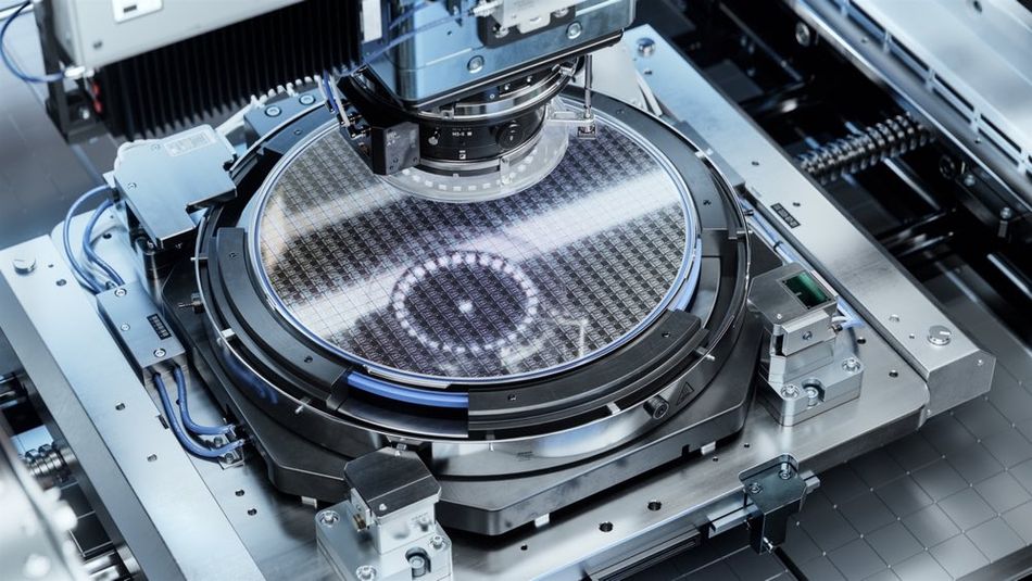
Once the foundry receives the GDSII file, it begins the process of creating the masks for production. These masks are used in the photolithography process to transfer the design onto the silicon wafer. The creation of the masks is a complex and time-consuming process, often taking several weeks to complete.
Further Reading: Chips and Wafers: Making of the semiconductor industry
Post-Tapeout Phase
The post-tapeout phase in semiconductor manufacturing begins after the design data has been sent to the foundry and the masks for production have been created. This phase involves the actual fabrication of the semiconductor device on the silicon wafer, followed by a series of tests to ensure the device functions as intended.
The fabrication process, also known as the front-end-of-line (FEOL) process, involves several steps including photomask application, etching, and ion implantation. Photolithography uses the masks created during the tapeout event to transfer the design onto the silicon wafer. Etching removes the unwanted material, and ion implantation alters the properties of the silicon to create the various components of the semiconductor device.
Following the fabrication process, the devices undergo a series of tests in the back-end-of-line (BEOL) process. These tests include electrical tests to verify the functionality of the device and physical inspections to check for defects. Any devices that fail these tests are discarded, while the successful ones proceed to packaging and final testing.
Manufacturing
The manufacturing process in semiconductor production involves the fabrication of the semiconductor devices on the silicon wafer and their subsequent testing, packaging, and final testing.
FEOL Process
This process begins with the front-end-of-line (FEOL) process, where the design is transferred onto the silicon wafer using photolithography, followed by etching and ion implantation.
Photolithography is a process that uses light to transfer the design from the mask onto the silicon wafer. This process creates a pattern on the wafer that corresponds to the design of the semiconductor device. Etching then removes the unwanted material from the wafer, leaving behind the desired pattern. Ion implantation alters the properties of the silicon to create the various components of the device, such as transistors and diodes.
Following the FEOL process, the devices undergo the back-end-of-line (BEOL) process. This involves a series of tests to verify the functionality of the devices and to check for defects. Electrical tests are conducted to ensure that the devices function as intended, while physical inspections are carried out to identify any defects or anomalies.
Devices that pass these tests are then packaged to protect them from environmental factors and to provide the necessary connections for their operation. The packaged devices undergo final testing to verify their performance and reliability before they are shipped to customers.
Testing
Testing and validation are critical stages in the post-tapeout phase of semiconductor manufacturing. These processes ensure that the fabricated semiconductor devices function as intended and meet the specified performance requirements.
The testing process involves conducting a series of electrical tests on the devices. These tests are designed to verify the functionality of the devices and to identify any defects or anomalies. The tests are conducted using automated test equipment (ATE), which can quickly and accurately test a large number of devices.
Recommended Reading: Flying Probe Test: An Extensive Guide to the Technology and Applications
Electrical tests include parametric tests, which measure the electrical properties of the devices, and functional tests, which verify that the devices operate as intended. Parametric tests measure parameters such as voltage, current, and resistance, while functional tests check the operation of the device under various conditions.
Validation
Validation, on the other hand, is a process that verifies that the devices meet the specified performance requirements. This involves testing the devices under real-world conditions to ensure that they perform as expected. Validation tests are typically more comprehensive and rigorous than the initial electrical tests and are designed to ensure that the devices are ready for market release.
Defective devices identified during the testing and validation processes are discarded, while the successful ones proceed to packaging and final testing. These processes are crucial to ensure the production of high-quality semiconductor devices and to maintain the reputation and reliability of the semiconductor manufacturer.
The Evolution of Tapeout
The tapeout process in semiconductor manufacturing has evolved significantly over the years, driven by advancements in technology and increasing complexity of semiconductor devices. In the early days of semiconductor manufacturing, the tapeout process was a physical event, where the design was transferred onto tape and sent to the foundry for fabrication. Today, the process is entirely digital, with the design data being sent electronically to the foundry.
The evolution of the tapeout process has also been influenced by the increasing complexity of semiconductor devices. As devices have become more complex, the number of design rules has increased, making the design rule checking (DRC) process more complex and time-consuming. Advances in software tools have helped to automate this process, but the complexity of the task continues to increase with each new generation of devices.
The increasing complexity of devices has also led to the development of new verification techniques. In addition to the traditional DRC and layout versus schematic (LVS) checks, new techniques such as electrical rule checking (ERC) and design for manufacturability (DFM) checks have been developed. These techniques help to ensure that the design is not only manufacturable, but also optimized for performance and yield.
A Historical Perspective of Tapeouts
The history of the tapeout process in semiconductor manufacturing is a reflection of the evolution of the semiconductor industry itself. In the early days of the industry, the design and fabrication processes were relatively simple, and the tapeout process was a straightforward event. However, as the industry has evolved, so too has the tapeout process.
In the 1980s and 1990s, as the complexity of semiconductor devices increased, the tapeout process became more complex. The number of design rules increased, and the process of checking the design against these rules became more time-consuming. At the same time, the cost of errors in the design increased, as any errors discovered after tapeout could lead to the need for a new set of masks, significantly increasing the costs.
In response to these challenges, the industry developed new software tools to automate the DRC process and to perform other verification checks. These tools have continued to evolve over the years, becoming more sophisticated and capable of handling the increasing complexity of semiconductor devices.
The tapeout process has also been influenced by changes in the manufacturing process. As the industry has moved towards smaller process nodes, the challenges of manufacturing have increased. This has led to the development of new verification techniques, such as DFM checks, to physical ensure that the design is not only manufacturable, but also optimized for the specific capabilities of the foundry.
The evolution of the tapeout process reflects the ongoing innovation and advancement in the semiconductor industry. As the industry continues to evolve, the tapeout process will continue to adapt and change, driven by the need to ensure the manufacturability and performance of increasingly complex semiconductor devices.
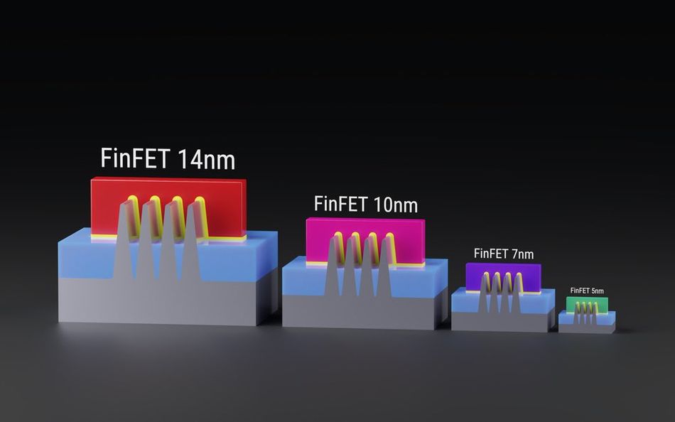
Tapeout and Moore's Law
Moore's Law has had a profound impact on the evolution of the tapeout process in semiconductor manufacturing. Moore's Law states that the number of transistors on a chip doubles approximately every two years. This prediction, made in 1965, has held true for over five decades and has driven the relentless pace of innovation in the semiconductor industry.
This has led to the development of more sophisticated design software and verification tools to manage this complexity. The increasing density of transistors also poses challenges for the fabrication process, as smaller feature sizes require more precise manufacturing techniques.
Moore's Law has also influenced the economic aspects of the tapeout process. As the complexity of the design increases, so too does the cost of the masks required for production. This has led to the so-called "mask cost explosion", where the cost of masks has been increasing at a faster rate than the revenue generated by the additional transistors. This economic challenge has led to the development of new design techniques and business models, such as multi-project wafers and design reuse, to mitigate the impact of rising mask costs.
Conclusion
The tapeout process in semiconductor manufacturing is a complex and critical phase that marks the transition from design to production. It involves the finalization of the design, the creation of the GDSII file, and the production of the masks for photolithography. The evolution of the tapeout process has been driven by advancements in technology, increasing complexity of semiconductor devices, and the economic implications of Moore's Law. Despite the challenges, the semiconductor industry has continually adapted and innovated, ensuring the continued advancement of semiconductor technology.
Frequently Asked Questions (FAQs)
1. What is the tapeout process in semiconductor manufacturing?
The tapeout process is the final stage in the design phase of semiconductor manufacturing. It involves finalizing the design, creating a GDSII file that contains the geometric descriptions of the layout, and sending this file to the foundry for the creation of the masks used in production.
2. What is the significance of the tapeout event?
The tapeout event is a significant milestone in semiconductor manufacturing as it represents the transition from design to production. It is the point at which the design of the semiconductor device is finalized and ready for fabrication.
3. How has the tapeout process evolved over time?
The tapeout process has evolved significantly over the years, from a physical event to a completely digital process. The increasing complexity of semiconductor devices has led to the development of more sophisticated design software and verification tools, and the introduction of new verification techniques such as electrical rule checking (ERC) and design for manufacturability (DFM) checks.
4. What is the impact of Moore's Law on the tapeout process?
Moore's Law, which states that the number of transistors on a chip doubles approximately every two years, has had a profound impact on the tapeout process. As the number of transistors increases, so does the complexity of the design and the number of design rules, leading to more sophisticated design software and verification tools. The increasing density of transistors also poses challenges for the fabrication process, requiring more precise manufacturing techniques.
References
in this article
1. What is Tapeout in Semiconductor Manufacturing?2. The Pre-Tapeout Phase3. The Tapeout Process4. Post-Tapeout Phase5. Manufacturing6. The Evolution of Tapeout7. A Historical Perspective of Tapeouts8. Tapeout and Moore's Law 9. Conclusion10. Frequently Asked Questions (FAQs)11. References