Ion Milling: A Comprehensive Guide to Material Etching Techniques
Ion milling is a material etching technique used extensively in modern manufacturing and research. It involves the bombardment of a sample with charged particles, called ions, to remove material from the surface in a controlled manner. This article explores the fundamental principles of ion milling, the various techniques used, the equipment required, and its applications in different fields.

12 May, 2023. 19 minutes read
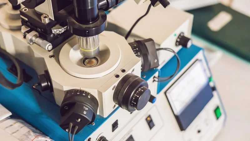
Ion Milling Machine
Introduction to Ion Milling
Ion milling has gained prominence due to its ability to etch highly precise materials, making it indispensable in areas requiring nano-scale fabrication or modification. This process is crucial for various industries, such as semiconductor manufacturing, materials science, and nanotechnology, where precise control over the material removal process is essential.
Ion milling is a material etching method that is widely employed in present-day manufacturing and research. It involves carefully removing material from the surface of a cross-section by bombarding it with charged particles known as ions. The technique offers several advantages, such as minimal sample damage, high resolution, and the capability to process a wide range of materials. Particularly on materials that are challenging to prepare by conventional metallography, such as zirconium, and zircalloy, ion milling can yield surfaces suitable for Electron Backscatter Diffraction (EBSD) with minimal prior preparation.
EBSD is frequently used to map the distribution and calculate the area fraction of phases in a sample. Phase discrimination may be simply based on crystallographic differences or may also take into account chemical data (from energy dispersive X-ray spectroscopy, or EDS).
Fundamental Principles of Ion Milling
Ion milling relies on the basic principles of physics, particularly those governing the interactions between charged particles and solid surfaces. The process involves directing a stream of ions, typically noble gas ions such as argon or xenon, toward the cross-section material's surface. As the ions collide with the surface, they transfer their kinetic energy to the target atoms, causing them to dislodge from the surface. This phenomenon, known as sputtering, leads to material removal from the surface and forms the basis of the ion milling process.
The efficiency of ion milling depends on several factors, including the incident ion energy, ion mass, angle of incidence, and the atomic properties of the target material. Understanding these factors and their influence on the milling process is crucial to optimizing ion milling parameters and achieving desired etching results. The following sections, explore ion milling principles in greater detail, starting with ion-solid interactions.[1]
Ion-Solid Interactions
Ion-solid interactions are central to the ion milling process. When ions collide with the target material's surface, they can penetrate the surface to a certain depth, depending on their energy and mass. As the ions penetrate the surface, they experience a series of collisions with the target atoms, transferring energy and momentum to them. These collisions can be categorized into two types: elastic and inelastic.
In elastic collisions, the ions interact with the target atoms via Coulombic forces without causing any electronic excitations or ionizations. The transfer of kinetic energy during elastic collisions leads to the displacement of target atoms from their lattice positions, and if the transferred energy is sufficient, it can cause sputtering. The sputtering yield, defined as the average number of atoms ejected per incident ion, is a crucial parameter in ion milling, as it determines the material removal rate.
In contrast, inelastic collisions involve energy transfer to the target atoms' electrons, resulting in electronic excitations or ionizations. These processes can lead to the generation of secondary electrons and may also contribute to chemical reactions on the surface, especially in reactive ion milling techniques.
The efficiency of ion milling and the quality of the etched surface depend on the balance between elastic and inelastic collisions. Understanding the factors that influence ion-solid interactions, such as ion energy, ion mass, and target material properties, is essential for optimizing ion milling parameters and achieving precise material removal.
Sputtering Yield
Sputtering yield is a crucial factor in ion milling because it measures material removal effectiveness. It is described as the average number of atoms expulsed from the target surface for each incident ion. The sputtering yield is influenced by some variables, such as the incident ion energy, mass, angle of incidence, and atomic characteristics of the target material. To optimize the ion milling procedure and obtain the desired etching results, it is crucial to have a solid understanding of these parameters.
One of the key factors influencing the sputtering yield is the incident ion energy. Typically, the sputtering yield increases with ion energy, reaching a maximum value before decreasing at higher energies. This behavior can be explained by considering the energy transfer between ions and target atoms during collisions. At low ion energies, the energy transfer is insufficient to displace target atoms from their lattice positions, leading to low sputtering yields. As ion energy increases, the energy transfer becomes more efficient, leading to a higher sputtering yield. However, at very high ion energies, the ions penetrate deeper into the target material, reducing the likelihood of energy transfer to surface atoms and subsequently decreasing the sputtering yield.
In addition, the mass of the incident ions also plays a crucial role in determining the sputtering yield. Heavier ions transfer more momentum to the target atoms during collisions, leading to a higher sputtering yield. However, as ion mass increases, the ion penetration depth into the target material also increases, which can reduce the sputtering efficiency at the surface.
The angle of incidence of the ions with respect to the target surface affects the sputtering yield as well. At normal incidence (0 degrees), the sputtering yield
Ion Milling Techniques
Various ion milling techniques have been developed to address specific needs and applications in different industries. These techniques primarily differ in the ion source, process gas composition, and operating conditions. Each method has its advantages and drawbacks, making it suitable for particular materials and applications. This section discusses the most common ion milling techniques, including reactive ion etching, focused ion beam milling, and ion beam sputtering.
Reactive Ion Etching
Reactive ion etching (RIE) is a widely used ion milling technique in semiconductor manufacturing and materials science. In addition to inert gases like argon, it entails employing chemically reactive process gases like halogen-containing chemicals or metal-organic precursors. By interacting with the target material and triggering chemical reactions at the surface, the reactive species in the gas mixture improve the etching process.
In RIE, plasma is generated by applying an electric field to the process gas mixture, ionizing the gas molecules and creating a high-density plasma consisting of ions, electrons, and neutral species. The reactive species in the plasma chemically react with the surface atoms, forming volatile by-products that can be easily pumped away. The energetic ions in the plasma also physically sputter the surface, contributing to the material removal process.
The primary advantage of RIE is its high selectivity, which is the ability to etch specific materials preferentially over others. This is achieved by carefully selecting the process gas composition and operating conditions, allowing precise control over the etching process. RIE also offers excellent etching uniformity and the ability to create anisotropic etch profiles, making it suitable for various applications such as semiconductor device fabrication, micro-electro-mechanical systems (MEMS), and nanotechnology. However, RIE can be more complex and expensive compared to other ion milling techniques due to the need for specialized gas handling systems and plasma generation equipment. [2]
Ion Beam Etching
Another popular ion milling technique is ion beam etching, commonly referred to as ion beam milling or ion beam sputtering. It removes material off the target surface by using a focussed, precisely defined beam of ions, often made of inert gas ions like argon. Ion beam etching, which differs from reactive ion etching in that it doesn't rely on chemically reactive gases, is a wholly physical sputtering process.
The ion beam is generated using an ion source, which can be a Kaufman-type ion source, an electron cyclotron resonance (ECR) source, or an inductively coupled plasma (ICP) source, among others. These ion sources produce a high-density, collimated beam of ions with well-controlled energy and direction. The ion beam is directed towards the target surface, where the energetic ions collide with the surface atoms, causing them to be sputtered away.
Ion beam etching offers several advantages, such as high etching rates, excellent depth control, and the ability to create anisotropic etch profiles. Since the process does not involve chemically reactive species, the etching process is relatively clean and less prone to contamination. Additionally, ion beam etching is compatible with a wide range of materials, making it suitable for various applications in microelectronics, optics, and materials science.
However, there are some challenges associated with ion beam etching, including the need for precise ion beam control and potential ion beam-induced damage to the target material. Moreover, ion beam etching systems can be more expensive and complex compared to other ion milling techniques due to the requirements for high-vacuum environments and sophisticated ion beam generation and control systems. Despite these challenges, ion beam etching remains a valuable tool in various industries, particularly when high precision and material compatibility are essential.
Focused Ion Beam Milling
Focused ion beam (FIB) milling is a highly precise ion milling technique that utilizes a finely focused beam of ions, usually gallium ions, to remove or modify the material on the target surface at the nanoscale level. Due to its exceptional precision and control, FIB milling has become an indispensable tool in various fields, including semiconductor manufacturing, materials science, and nanofabrication.
In FIB milling, a liquid metal ion source (LMIS) is used to generate a focused ion beam. The LMIS typically consists of a sharp needle made of a gallium alloy, which is heated to create a liquid metal film at the needle's tip. An electric field is applied to extract and accelerate the ions from the liquid metal film, forming a highly focused ion beam. The ion beam is then directed towards the target surface using magnetic and electrostatic lenses, enabling precise control over the milling process.
The high-energy gallium ions in the FIB interact with the target material, causing atoms to be sputtered away. Due to the extremely fine focus of the ion beam, FIB milling can achieve lateral resolutions down to a few nanometers, enabling the creation of intricate structures and patterns on the target surface. FIB milling is also a versatile technique, capable of milling a wide range of materials, including metals, semiconductors, and insulators.
One of the significant advantages of FIB milling is its ability to perform both material removal and deposition processes. By introducing a gas precursor into the FIB chamber, it is possible to deposit materials onto the target surface, enabling the fabrication of complex three-dimensional structures. This combination of milling and deposition capabilities makes FIB an invaluable tool for prototyping, failure analysis, and modification of semiconductor devices and other nanostructures.
However, there are some limitations to FIB milling, such as the relatively slow milling rates and the potential for ion-induced damage to the target material. Additionally, the use of gallium ions can result in the unintentional doping of certain materials, which may affect their electrical properties. Despite these drawbacks, FIB milling remains an essential technique in various research and industrial applications, where its unparalleled precision and control are crucial.[3]
Ion Milling Equipment
Ion milling equipment is crucial for the successful implementation of ion milling processes. The equipment plays a significant role in determining the quality, precision, and efficiency of the milling process. This section discusses the essential components of ion milling equipment, including ion sources, ion optics systems, and sample holders, along with the various types of equipment available for different ion milling techniques.
Ion Sources
Ion sources are a critical component of ion milling equipment, as they generate the ions that are used for milling the target material. There are several types of ion sources used in ion milling processes, each with its specific advantages and limitations.
Liquid Metal Ion Source (LMIS): An LMIS is widely used in Focused Ion Beam (FIB) systems, where high beam current densities and fine focusing capabilities are required. In an LMIS, a needle made of gallium alloy is heated to form a liquid metal film at its tip. An electric field extracts and accelerates ions from the liquid metal film, creating a highly focused ion beam. The primary advantage of LMIS is its ability to generate a stable, finely focused ion beam with a small energy spread.
Radio Frequency (RF) Ion Source: RF ion sources are commonly employed in broad-beam ion milling systems, such as reactive ion etching and ion beam etching. In an RF ion source, a radio frequency signal is applied to a gas-filled chamber, generating plasma through the ionization of the gas molecules. Ions are extracted from the plasma and accelerated towards the target material by an electric field. RF ion sources can produce a wide range of ion species by selecting the appropriate gas, making them suitable for various applications.
Duoplasmatron Ion Source: The Duoplasmatron ion source is another type of ion source used in broad-beam ion milling systems. It operates by creating a high-pressure plasma in a discharge chamber and extracting ions through an extraction aperture. The extracted ions are then accelerated by an electric field. Duoplasmatron ion sources are known for their high ion current densities, which can be advantageous for applications requiring high material removal rates.
Each ion source type has specific characteristics, such as ion energy distribution, ion current density, and ion species availability, which can significantly impact the ion milling process. Therefore, selecting the appropriate ion source is crucial for achieving the desired results in a given application.
Vacuum Systems
Vacuum systems are a fundamental part of ion milling equipment, as they create and maintain the low-pressure environment required for the ion milling process. The quality of the vacuum directly affects the performance and efficiency of the ion milling process, making it an essential component for achieving precise and consistent results. This section will discuss the role of vacuum systems in ion milling, the key components involved, and the types of vacuum pumps commonly used.
The primary purpose of a vacuum system in ion milling is to remove air and other contaminants from the milling chamber, which minimizes the scattering of ions and reduces the likelihood of unwanted chemical reactions between ions and residual gas molecules. A high-quality vacuum also reduces the potential for sample contamination, ensuring the reliability of the final results.
A typical vacuum system in ion milling equipment consists of several components, including vacuum pumps, vacuum chambers, and vacuum gauges. The vacuum pumps create and maintain the desired vacuum level, while the vacuum chamber houses the ion source, ion optics, and sample holder. Vacuum gauges are used to monitor the pressure within the chamber, ensuring that it remains within the optimal range for the ion milling process.
There are various types of vacuum pumps employed in ion milling equipment, each with its unique characteristics and capabilities. The most commonly used vacuum pumps in ion milling are:
Rotary Vane Pumps: Rotary vane pumps are mechanical pumps that use rotating vanes to create a vacuum by trapping and compressing gas molecules. They are known for their durability and ease of maintenance, making them a popular choice for achieving moderate vacuum levels in ion milling systems.
Turbo-molecular Pumps: Turbo-molecular pumps operate on the principle of rapidly rotating blades that transfer momentum to gas molecules, effectively pumping them out of the vacuum chamber. They are capable of achieving high vacuum levels and are often used in combination with rotary vane pumps to provide the low-pressure environment needed for ion milling processes.
Cryo-pumps: Cryo-pumps utilize extremely low temperatures to condense and capture gas molecules on a cold surface, effectively removing them from the vacuum chamber. Cryo-pumps are advantageous in applications where ultra-high vacuum levels are required or when dealing with reactive gases, as they do not introduce any contaminants into the vacuum chamber.
The choice of the vacuum pump depends on factors such as the required vacuum level, the type of ion milling technique being used, and the specific requirements of the application. A carefully designed and well-maintained vacuum system is crucial for the successful implementation of ion milling processes and for achieving high-quality results.
Sample Holders
Sample holders play a crucial role in ion milling processes, as they ensure that the material being processed is accurately positioned, securely held, and properly cooled. The choice of an appropriate sample holder can greatly influence the quality and consistency of the ion milling results. This section will discuss the importance of sample holders, their design features, and the materials used in their construction.
The main function of a sample holder is to maintain the sample(cross-section) in a precise position relative to the ion beam, allowing for uniform and controlled milling across the entire surface. Proper positioning is essential for achieving the desired milling depth and ensuring that the sample remains flat and undistorted throughout the process. Additionally, sample holders must be designed to minimize any vibrations or movements that could negatively impact the milling accuracy.
Another critical aspect of sample holders is their ability to provide thermal management during the ion milling process. Ion milling can generate significant heat, which can cause sample damage or distortion if not effectively managed. Sample holders often include cooling mechanisms, such as integrated water or gas cooling channels, to dissipate the heat generated during milling and protect the sample from thermal damage.
Sample holders are typically constructed from materials that exhibit high thermal conductivity, mechanical stability, and chemical inertness. Commonly used materials include:
Aluminum: Aluminum is a popular choice for sample holders due to its high thermal conductivity, lightweight, and affordability. Its excellent heat dissipation properties make it suitable for applications where efficient cooling is required. However, aluminum can be prone to corrosion and may not be ideal for use with highly reactive ion species.
Stainless Steel: Stainless steel is another frequently used material for sample holders, offering excellent mechanical strength and corrosion resistance. While its thermal conductivity is lower than that of aluminum, stainless steel can still provide adequate cooling performance in most ion milling applications.
Ceramics: Ceramic materials, such as alumina and silicon carbide, offer outstanding chemical inertness and high-temperature resistance. Their low thermal conductivity can be advantageous in certain applications, as it helps to isolate the sample from external heat sources. However, ceramics can be more brittle and prone to breakage compared to metals, which can be a concern in high-vibration environments.
The choice of sample holder material and design depends on the specific requirements of the ion milling process, including the type of material being processed, the desired milling depth, and the thermal management needs. A well-designed sample holder is essential for achieving accurate, consistent, and high-quality ion milling results.
Applications of Ion Milling
Ion milling systems are frequently employed in the preparation of cross-section samples for scanning electron microscope (SEM), having applications in the study of semiconductors and materials, due to their ability to provide precise and controlled material removal. For instance, A conventional scanning electron microscope (SEM) uses a single beam to collect data from a sample, imaging it with electrons and analyzing it with X-rays. While the SEM performs high-resolution imaging, the focused ion beam-scanning electron microscope (FIB-SEM) adds a second beam, the ion beam, to cut into the material. Using this technique, you may create a 3D data stack that layers-by-layer represents your sample at the nanometer level.
In industries where precise and elaborate patterning or surface modification are necessary, its adaptability and high-resolution capabilities make it a preferred technology. This section explores some of the key applications of ion milling, starting with semiconductor manufacturing.
Semiconductor Manufacturing
One of the most significant applications of ion milling is in the manufacturing of semiconductor devices, such as integrated circuits (ICs) and microelectromechanical systems (MEMS). The fabrication of these devices involves the creation of intricate patterns and structures on the nanometer scale, which requires precise material removal techniques.
In semiconductor manufacturing, ion milling is often employed for etching and patterning processes. Reactive ion etching (RIE) and deep reactive ion etching (DRIE) are two widely used techniques in the industry. These techniques allow for the creation of high-resolution patterns with vertical sidewalls and excellent depth control, which are crucial for the fabrication of multilayered devices and three-dimensional structures.
One specific example of ion milling in semiconductor manufacturing is the creation of transistor gates. In this process, a thin layer of material (often a metal or metal oxide) is deposited onto a semiconductor substrate, and then selectively etched using ion milling to form the gate structure. The gate's dimensions and shape have a direct impact on the performance and functionality of the transistor, making precision and control of the utmost importance.
Another application in semiconductor manufacturing is the formation of trenches and vias, which are used to interconnect different layers within an integrated circuit. Ion milling techniques, such as DRIE, enable the creation of deep, high-aspect-ratio trenches with excellent sidewall smoothness and verticality. This is essential for minimizing signal loss and ensuring reliable connections between layers.
Ion milling is also employed in the fabrication of MEMS devices, which are miniature mechanical and electrical components integrated into a single chip. MEMS devices have diverse applications, including sensors, actuators, and microfluidic systems. The fabrication of these devices often involves the creation of intricate, three-dimensional structures with high aspect ratios and tight tolerances, which can be achieved using ion milling techniques.
In summary, ion milling plays a crucial role in semiconductor manufacturing, enabling the fabrication of high-resolution, complex structures that are essential for the performance and functionality of modern electronic devices. Its precision and control make it an indispensable tool in this highly demanding and technologically advanced field.
Materials Science and Engineering
Ion milling is an essential tool in the field of materials science and engineering, as it provides a means to analyze, modify, and characterize various materials at the microscopic and nanoscopic levels. In this section, we will discuss some of the key applications of ion milling in materials science and engineering, focusing on cross-section preparation, thin film deposition, and surface modification.
Sample preparation is a critical step in materials analysis, as it enables researchers to obtain accurate and reliable data from techniques such as electron microscopy, X-ray diffraction, and atomic force microscopy. Ion milling is often employed for the preparation of thin, electron-transparent specimens for transmission electron microscopy (TEM). These specimens need to be extremely thin (typically around 100 nm or less) to allow electrons to pass through the material and generate high-resolution images. Focused ion beam (FIB) milling is a popular method for this purpose, as it enables precise control over the sample's thickness and uniformity while minimizing damage and contamination.
Ion milling also plays a vital role in the deposition of thin films, which are used in a wide range of applications, including electronic devices, optical coatings, and protective layers. Ion beam-assisted deposition (IBAD) is a technique that combines ion milling with physical vapor deposition (PVD) to create high-quality thin films with excellent adherence, density, and uniformity. In IBAD, an ion beam simultaneously bombards the substrate while the material is being deposited, promoting adhesion and reducing defects such as voids and pinholes. The resulting films exhibit improved mechanical, electrical, and optical properties, making them suitable for demanding applications.
Surface modification is another important application of ion milling in materials science and engineering. By bombarding a material's surface with ions, it is possible to alter its physical and chemical properties, such as roughness, wettability, hardness, and corrosion resistance. For example, ion implantation can be used to introduce dopants or impurities into a material, thereby modifying its electrical conductivity and other properties. This technique is widely used in the semiconductor industry for the fabrication of doped layers and junctions in electronic devices. Ion milling can also be employed to create surface textures or patterns, which can enhance a material's performance in applications such as tribology, catalysis, and biocompatibility.
In conclusion, ion milling is a versatile and powerful tool in the realm of materials science and engineering, offering unique capabilities for the analysis, modification, and characterization of various materials. Its precision and control make it an indispensable technique for researchers and engineers working to develop and optimize advanced materials for a wide range of applications.
Nanotechnology
Nanotechnology is an interdisciplinary field that deals with the manipulation and control of matter at the atomic and molecular scale, typically ranging from 1 to 100 nanometers. Ion milling is an indispensable technique in the field of nanotechnology, as it allows for precise structuring, modification, and characterization of materials at the nanoscale. In this section, we will discuss the applications of ion milling in the creation of nanostructures, the fabrication of nanodevices, and the study of nanoscale phenomena.
One of the main applications of ion milling in nanotechnology is the creation of nanostructures, which are structures with dimensions in the nanometer range. Focused ion beam (FIB) milling is particularly suited for this task, as it enables precise patterning of materials with nanometer-scale resolution. For example, FIB milling can be employed to create nanopillars, nanochannels, and nanowires with dimensions as small as a few tens of nanometers. These nanostructures have unique physical, chemical, and optical properties that can be exploited in a wide range of applications, including sensors, catalysts, and photonic devices.
Ion milling is also essential for the fabrication of nanodevices, which are devices with functional components on the nanometer scale. In the semiconductor industry, for instance, ion implantation is used to create doped regions and junctions in transistors and other electronic components, enabling the miniaturization of integrated circuits to the nanoscale. Moreover, ion milling techniques such as reactive ion etching (RIE) and ion beam etching (IBE) are employed to define and shape the features of these nanoscale components, allowing for the fabrication of complex devices with high integration density and performance.
The study of nanoscale phenomena is another important application of ion milling in the field of nanotechnology. Ion milling techniques can be employed to prepare ultrathin specimens for advanced characterization techniques, such as high-resolution transmission electron microscopy (HRTEM) and scanning tunneling microscopy (STM). These techniques enable researchers to investigate the atomic and electronic structure of materials at the nanoscale, leading to a better understanding of phenomena such as quantum confinement, surface plasmons, and molecular self-assembly.
In summary, ion milling is a critical tool in the field of nanotechnology, as it provides the means to create, modify, and analyze materials at the nanometer scale. The precision and control offered by ion milling techniques enable the development of advanced nanostructures and nanodevices, as well as the investigation of fundamental nanoscale phenomena. As nanotechnology continues to advance, ion milling will remain an essential technique for researchers and engineers working at the forefront of this rapidly evolving field.[4]
Conclusion
Ion milling is a versatile and powerful technique used in various industries and research fields. Its ability to provide precise material removal and patterning has led to significant advancements in semiconductor manufacturing, materials science, nanotechnology, and other areas. As technology continues to evolve and demands for higher precision and smaller features grow, ion milling will remain a vital tool for scientists and engineers working on the cutting edge of their respective fields.
Frequently Asked Questions (FAQs)
Q: What are the main types of ion milling techniques?
A: The primary ion milling techniques include reactive ion etching (RIE), ion beam etching (IBE), and focused ion beam (FIB) milling. Each of these techniques has its advantages and disadvantages, making them suitable for different applications and materials.
Q: What are some applications of ion milling?
A: Ion milling is used in a variety of applications, such as semiconductor manufacturing, materials science, and nanotechnology. It is employed for creating nanostructures, fabricating nanodevices, and studying nanoscale phenomena. Ion milling is also used to prepare samples for advanced characterization techniques, like high-resolution transmission electron microscopy (HRTEM) and scanning tunneling microscopy (STM).
Q: What is the main difference between reactive ion etching and ion beam etching?
A: Reactive ion etching (RIE) combines the use of ions and reactive gas species to achieve highly anisotropic etching, while ion beam etching (IBE) employs a directed ion beam to remove material without the use of reactive gases. RIE provides better control over the etching profile but may introduce more chemical damage to the material, whereas IBE offers a more gentle approach with less chemical damage but may result in less anisotropic etching.
Q: How does focus ion beam milling work?
A: Focused ion beam (FIB) milling utilizes a finely focused beam of ions, typically gallium ions, to remove material from a surface in a highly controlled manner. The ion beam can be manipulated to create intricate patterns and structures with nanometer-scale resolution, making it ideal for fabricating nanostructures and nanodevices, as well as preparing samples for advanced characterization techniques.
Q: What types of ion sources are used in ion milling?
A: Ion sources for ion milling can be categorized into three main types: electron impact ion sources, plasma-based ion sources, and ion liquid sources. Electron-impact ion sources generate ions by accelerating electrons into a gas, while plasma-based ion sources create plasma by applying an electric or magnetic field to a gas. Ion liquid sources generate ions by applying an electric field to a liquid metal or alloy. The choice of ion source depends on factors such as the desired ion species, energy, and current density.
References
Yuki Inagi (2023). Hitachi's State-of-the-Art Ion Milling Systems. Available at: https://www.hitachi-hightech.com/global/en/sinews/technical_explanation/100302/ [Accessed 6th May 2021].
Venus Kohli, Wevolver (2023). Reactive Ion Etching: A Comprehensive Guide. Available at: https://www.wevolver.com/article/reactive-ion-etching-a-comprehensive-guide [Accessed 6th May 2021].
AZO Materials (2012). An Introduction to Ion Beam Etching. Available at: https://www.azom.com/article.aspx?ArticleID=7533 [Accessed 7th May 2021].
Yuki Inagi (2023). Hitachi's State-of-the-Art Ion Milling Systems. Available at: https://www.hitachi-hightech.com/global/en/sinews/technical_explanation/100302/ [Accessed 7th May 2021].