System in Package: A Comprehensive Guide to SiP Technology
This article provides a detailed guide to System in Package technology, its advantages and challenges, key components, design, and manufacturing process.

18 Jul, 2023. 14 minutes read
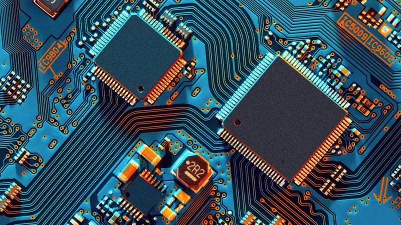
Electronic circuit board with SiP technology
Introduction
System in Package (SiP) technology has emerged as a critical innovation in modern electronics, offering numerous advantages over traditional methods. SiP technology uses semiconductors to create integrated packages containing multiple ICs and passive components, creating compact and high-performance devices. This technology has widespread adoption across various industries, including consumer electronics, automotive, aerospace, and medical devices. By leveraging System in Package technology, designers and manufacturers can achieve higher levels of integration, improved power efficiency, and reduced time-to-market for their products.
Overview of System in Package (SiP) Technology
System in Package (SiP) technology has been around since the 1980s in the form of multi-chip modules. [1] In the 1970s, it was in the form of discretionary wiring, multi-chip modules (MCMs), and hybrid integrated circuits (HICs). In the 1990s, SiP was used as a solution for Intel’s Pentium Pro3 integrated processor and cache. SiP technology has become increasingly popular in various industries, such as consumer electronics, automotive, aerospace, and medical devices.

The adoption of SiP technology can be attributed to several factors, including the need for miniaturization, increased performance, and reduced power consumption. By integrating multiple components into a single package, SiP technology enables designers and manufacturers to create devices with a smaller form factor, reduced weight, and improved reliability. SiP methodology can reduce the overall size of a given system by as much as 65%. The global system in package (SiP) technology market size was valued at $14.8 billion in 2020, and is projected to reach $34.2 billion by 2030, growing at a CAGR of 9.7% from 2021 to 2030. [2]
One of the key advantages of SiP technology is its ability to facilitate the integration of heterogeneous components, such as analog, digital, and mixed-signal ICs, as well as passive components like resistors, capacitors, and inductors. This level of integration allows for the creation of highly complex systems that can perform a wide range of functions while maintaining a small footprint.
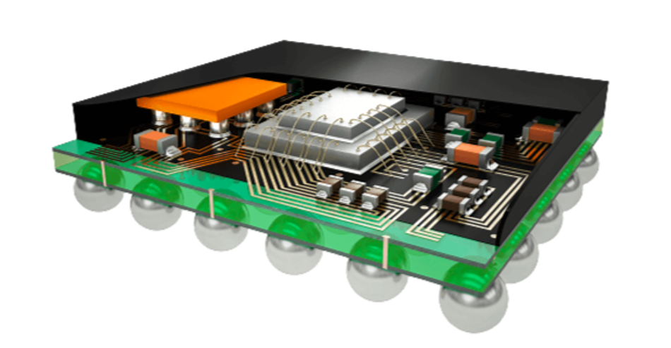
 device; Credits: octavosystems")
MEMS stands for Microelectromechanical Systems. It is a technology that integrates mechanical elements, sensors, actuators, and electronics on a single chip. MEMS devices are used in a variety of applications, including smartphones, laptops, medical devices, and industrial automation. SiP and MEMS can be used together to create devices that are smaller, lighter, and more powerful than devices that use only one technology. For example, a SiP with a MEMS sensor can be used to create a device that is smaller and lighter than a device that uses a separate sensor and IC.
SiP solutions offer a powerful technology for creating compact, high-performance devices with many applications. By integrating multiple components into a single package, SiP technology enables designers and manufacturers to achieve higher levels of integration, improved power efficiency, and reduced time-to-market for their products.
SiP vs. System on Chip (SoC)
System in Package (SiP) and System on Chip (SoC) are two distinct approaches to integrating electronic components and systems. While both technologies aim to achieve higher levels of integration and miniaturization, they differ in design principles, implementation, and applications.
 vs. System on Chip (SoC)")
SiP technology involves the integration of multiple ICs, and passive components into a single package. This approach combines various functional blocks within a compact form factor, such as processors, memory, and sensors. SiP designs often utilize heterogeneous components, which can be manufactured using different process technologies and assembled together. This flexibility enables designers to optimize each component for its specific function, improving overall system performance. [3]
On the other hand, a System on Chip (SoC) integrates all the necessary components of an electronic system onto a single silicon die. This approach offers higher integration levels than SiP, as all the functional blocks are fabricated on the same substrate. However, SoC designs typically require a homogeneous manufacturing process, which can limit the flexibility and optimization of individual components.
Advantages of SiP Technology

SiP technology offers several advantages over traditional integration methods and SoC designs. These benefits include:
Design Flexibility: SiP allows combining the components manufactured using different process technologies, enabling designers to select the best-suited components for each function. This flexibility can improve performance, power efficiency, and cost optimization.
Reduced Time-to-Market: By leveraging pre-validated components and subsystems, SiP designs can significantly reduce the time required for product development and validation. This advantage enables manufacturers to bring new products to market more quickly, providing a competitive edge in fast-paced industries.
Compact Form Factor: SiP technology enables the integration of multiple components into a single package, resulting in a smaller overall footprint. This miniaturization is particularly beneficial for portable and wearable devices, where space constraints are a critical design consideration.
Improved System Performance: By integrating multiple components into a single package, SiP designs can reduce the parasitic effects and signal degradation associated with long interconnects. This improvement can enhance system performance, particularly in high-speed and high-frequency applications.
Cost Savings: SiP technology can offer cost savings by reducing the number of discrete components and printed circuit board (PCB) layers required for a given design. SiPs also reduce the number of layers required in a PCB by 33% to 50%. [4] Additionally, SiP designs can simplify the assembly process, further reducing manufacturing costs.
Recommended Reading: Low power SiP with integrated LTE-M NB-IoT modem and GPS
Challenges and Limitations of SiP Technology
Despite its numerous advantages, SiP technology faces challenges and limitations that may affect its adoption in specific applications or industries. One of the primary challenges is the increased design complexity. As SiP integrates multiple components into a single package, the design process becomes more intricate, requiring advanced design rules and methodologies to ensure proper functionality and performance.
Thermal management is another critical concern in SiP technology. As components are densely packed within the package, heat dissipation becomes more complex, potentially leading to overheating and reduced reliability. Designers must carefully consider thermal management solutions, such as heat sinks or thermal vias, to maintain optimal operating temperatures for the components within the SiP.
Signal integrity is also a significant challenge in SiP designs. The proximity of components and interconnects can lead to signal interference and crosstalk, which may degrade the system's overall performance. To mitigate these issues, designers must carefully plan the layout and routing of signals and consider the use of shielding techniques to minimize electromagnetic interference (EMI). [5]
Supply chain management can be another limitation of SiP technology. As SiP designs often require components from multiple suppliers, coordinating the procurement and assembly of these components can be complex and time-consuming. This may result in longer lead times and increased costs, particularly for smaller manufacturers with limited resources.
Finally, the testing and verification of SiP designs can be more challenging compared to traditional PCB-based systems. Due to the high level of integration, it may be difficult to isolate and test individual components within the SiP, potentially leading to increased testing time and costs. Designers must develop robust testing strategies to ensure the reliability and performance of the final product.
Key Components of a System in Package
A typical System in Package consists of several essential components that work together to form a complete system within a single package. These components include transistors, ICs, passive components, and interconnect technologies. Each component plays a crucial role in the overall performance and functionality of the SiP, and their selection and integration are critical to the design's success.
Integrated Circuits (ICs)
Integrated circuits (ICs) are the primary building blocks of a SiP, providing the system's core functionality and processing capabilities. ICs can be classified into various categories, such as digital, analog, and mixed-signal, depending on their function and the type of signals they process. Some common types of IC used in SiP designs include microprocessors, memory chips, sensors, and power management circuits.
The selection of ICs for a specific SiP application depends on several factors, including the desired functionality, performance requirements, power consumption, and cost constraints. Designers must carefully consider these factors when choosing the appropriate ICs for their SiP design, as the choice of ICs can significantly impact the overall system performance, efficiency, and reliability. [6]
In addition to selecting the right ICs, designers must also consider the integration of these components within the SiP. This involves determining the optimal layout and interconnect strategy to ensure proper signal routing and minimize potential issues such as signal interference and crosstalk. Furthermore, designers must also address thermal management concerns, as the close proximity of ICs within the SiP can lead to increased heat generation and potential overheating issues.
Recommended Reading: Types of IC Packages: A Comprehensive Guide
Passive Components
Passive components are crucial in SiP technology, providing essential functions such as filtering, energy storage, and impedance matching. These components do not generate or amplify signals but instead interact with them in various ways to ensure proper system operation. Some of the most common passive components used in SiP designs include resistors, capacitors, and inductors.
Resistors control the flow of current within a circuit, providing a specified amount of resistance to the passage of electrical current. They are essential for tasks such as voltage division, current limiting, and biasing of active components. In SiP designs, resistors can be integrated as thin-film or thick-film components or discrete surface-mount devices (SMDs).
Capacitors store electrical energy in an electric field and release it when needed. They are commonly used for electronic circuit filtering, energy storage, and decoupling. In SiP designs, capacitors can be integrated as multi-layer ceramic capacitors (MLCCs), tantalum capacitors, or other types of capacitors, depending on the application's specific requirements.
Inductors store energy in a magnetic field and are often used for filtering, energy storage, and impedance matching in electronic circuits. SiP designs can integrate inductors as wire-wound or thin-film components or as discrete SMDs.
The selection of passive components for a specific SiP application depends on various factors, such as the desired performance characteristics, size constraints, and cost considerations. Designers must carefully consider the trade-offs between these factors when choosing the appropriate passive components for their SiP designs. For example, high-performance capacitors may offer improved filtering capabilities but may be larger and more expensive than lower cost and performance alternatives. By carefully balancing these factors, designers can optimize the overall performance and cost of their SiP designs.
Interconnect Technologies
Interconnect technologies play a crucial role in SiP technology, as they enable the communication and data transfer between the various components within the package. These technologies are responsible for connecting the ICs and passive components, ensuring the proper functioning of the overall system. Several types of interconnect technologies are commonly used in SiP designs, each with advantages and challenges.
Wire bonding is a widely used interconnect technology in SiP designs, where thin wires connect the ICs and other components to the package substrate. Wire bonding offers a cost-effective interconnecting solution with relatively simple manufacturing processes. However, wire bonding can have signal speed and density limitations, making it less suitable for high-frequency or high-performance applications.
Through-silicon vias (TSVs) represent an advanced interconnect technology used in SiP designs, particularly for 3D integration. TSVs are vertical electrical connections that pass through the silicon substrate, enabling the stacking of multiple ICs within a single package. This approach offers significant interconnect density, signal speed, and power efficiency advantages. However, TSV technology is still relatively new and more complex and expensive than other interconnect methods.
When selecting an interconnect technology for a specific SiP application, designers must consider performance requirements, cost constraints, and manufacturing capabilities. Each interconnect technology has its advantages and challenges, and the optimal choice will depend on the specific needs of the application and the goals of the overall system design.
SiP Design and Manufacturing Process
The SiP design and manufacturing process involves several key steps, from the initial concept and component selection to the final assembly and testing of the completed package. Throughout this process, designers and manufacturers must address various challenges and considerations to ensure the successful implementation of SiP technology in their products.
SiP Design Tools and Methodologies
The design of a SiP requires advanced tools and methodologies to manage the complexity of integrating multiple components into a single package. These tools enable designers to create, simulate, and optimize their SiP designs, ensuring proper functionality and performance.
 software")
Some popular SiP design tools include electronic design automation (EDA) software, which provides a comprehensive suite of capabilities for schematic capture, layout, interface, and simulation. EDA tools allow designers to model and analyze their SiP designs, identifying potential issues and optimizing performance before moving to the manufacturing stage.
In addition to EDA tools, designers may employ specialized SiP design methodologies, such as co-design and design-for-manufacturability (DFM) techniques. Co-design involves the simultaneous design of multiple components within the SiP, ensuring that each component is optimized for its specific function and the overall system performance. DFM techniques focus on optimizing the SiP design for ease of manufacturing, reducing potential assembly issues, and improving yield rates.
The choice of design tools and methodologies can significantly impact the success of a SiP project, as they directly influence the final product's quality, performance, and manufacturability. Designers must carefully consider their options and select the most appropriate tools, and methodologies for their specific SiP application.
SiP Assembly and Packaging Techniques
The assembly and packaging of a System in Package play a crucial role in determining the overall performance, reliability, and form factor of the final product. Various techniques are used in SiP manufacturing, each with advantages and disadvantages. The selection of a specific assembly and packaging technique depends on factors such as the complexity of the design, the required performance characteristics, and cost constraints.

Flip Chip: Flip chip is an advanced SiP assembly technique that involves attaching the ICs directly to the substrate using solder bumps. [7] This method eliminates the need for wire bonding, improving signal integrity and reducing parasitic effects. Flip chip technology enables higher levels of integration and a more compact form factor than wire bonding. However, it can be more complex and expensive to implement, particularly for designs with many components.
Embedded Component Packaging: In this technique, components are embedded within the substrate, allowing for a highly integrated and compact design. This approach can offer significant advantages regarding form factor, thermal management, and signal integrity. However, it can be more complex and costly to implement than other assembly techniques and may require specialized equipment and processes.
System-in-Package-on-Package (SiP-PoP): SiP-PoP is a technique that involves stacking multiple SiP modules on top of each other, connected through high-density interconnects. This approach enables the integration of many components within a compact form factor, making it suitable for applications with stringent space constraints. However, SiP-PoP can be more complex and expensive to implement and may present challenges in thermal management and signal integrity.
When selecting an assembly and any advanced packaging technique for a SiP design, designers must carefully consider the trade-offs between performance, form factor, complexity, and cost. The choice of technique will depend on the application's specific requirements and the final product's desired characteristics.
Recommended Reading: PCBA Signal Integrity Problems: Ten Factors to Consider
4.3. SiP Testing and Verification
Testing and verification are critical aspects of the SiP manufacturing process, as they ensure the reliability and performance of the final product. Due to the high level of integration in SiP designs, testing, and verification can be more challenging compared to traditional PCB-based systems. Designers must develop robust testing strategies to address these challenges and ensure the successful deployment of SiP technology.
One of the primary challenges in SiP testing and verification is the difficulty in isolating and testing individual components within the package. The close proximity of components and interconnects can make it challenging to identify and diagnose potential issues, such as signal integrity problems or manufacturing defects. To overcome this challenge, designers may employ various testing methods, such as built-in self-test (BIST) techniques, which enable the components to perform self-diagnostics and report their status.
Another challenge in SiP testing and verification is the need to test the system at various stages of the manufacturing process. This may include package-level testing, final system-level testing, and wafer-level packaging and testing. Each testing stage requires different test equipment and methodologies, adding complexity and cost to the overall testing process. Designers must carefully plan their testing strategy to ensure comprehensive coverage while minimizing manufacturing time and cost impact.
Thermal and mechanical stress testing are also essential aspects of SiP verification. Due to the high level of integration and the close proximity of components, SiP designs can be more susceptible to thermal and mechanical stress-related issues. Designers must perform rigorous stress testing to ensure the reliability and robustness of the SiP under various operating conditions and environments.
In summary, SiP testing and verification present unique challenges due to the designs' high level of integration and complexity. Designers must develop robust testing strategies and employ advanced testing techniques to ensure the reliability and performance of SiP technology in various applications. By addressing these challenges, SiP technology can continue delivering the benefits of miniaturization, performance, and efficiency to various industries and applications.
Conclusion
System in Package technology has emerged as a powerful solution for creating compact, high-performance electronic devices. By integrating multiple components, such as integrated circuits (ICs), passive components, and interconnect technologies, into a single package, SiP enables designers and manufacturers to achieve higher levels of integration, improved power efficiency, and reduced time-to-market for their products. Despite some challenges and limitations, SiP technology continues to gain traction across various industries, including consumer electronics, automotive, aerospace, medical and mobile devices, offering numerous advantages over traditional integration methods and System on Chip (SoC) designs.
Frequently Asked Questions (FAQs)
1. What is the main difference between SiP and SoC?
A. SiP (System in Package) integrates multiple ICs and passive components into a single package. In contrast, SoC (System on Chip) integrates all the necessary components of an electronic system onto a single silicon die. SiP allows for the combination of various functional blocks and heterogeneous components, whereas SoC designs typically require a homogeneous manufacturing process.
2. What are the key advantages of SiP technology?
A. Some key advantages of SiP technology include design flexibility, reduced time-to-market, compact form factor, improved system performance, and cost savings.
3. What are the main challenges and limitations of SiP technology?
A. The main challenges and limitations of SiP technology include increased design complexity, thermal management, signal integrity, supply chain management, and testing and verification.
4. What are the common types of interconnect technologies used in SiP designs?
A. Common interconnect technologies used in SiP designs include wire bonding, flip-chip, and through-silicon vias (TSVs).
5. How does SiP technology contribute to miniaturization in electronic devices?
A. By integrating multiple components into a single package, SiP technology enables the creation of devices with a smaller form factor, reduced weight, and improved reliability. This miniaturization is particularly beneficial for portable and wearable devices, where space constraints are a critical design consideration.
References
1. Semiengineering. System In Package (SiP). [Cited 2023 July 10] Available at: Link
2. Alliedmarketresearch. System in Package (SiP) Technology Market Size [Cited 2023 July 10] Available at: Link
3. Anysilicon. Introduction to System in Package (SiP) [Cited 2023 July 10] Available at: Link
4. Octavosystems. SiP Technology [Cited 2023 July 10] Available at: Link
5. Ieeexplore. Research on SiP Signal Integrity Based on Ansys SIwave in Wearable Medical Systems. Industrial I/O [Cited 2023 July 10] Available at: Link
6. semiengineering. System In Package (SiP) [Cited 2023 July 10] Available at: Link
7. Wikipedia. Flip chip [Cited 2023 July 10] Available at: Link