IC Package Types: A Comprehensive Guide
Integrated circuit (IC) package types encompass a range of protective enclosures designed to shield semiconductor components from physical damage and corrosion. This article explores the various classifications of IC packages, each tailored to specific requirements and applications.

Last updated on 11 Apr, 2024. 15 minutes read
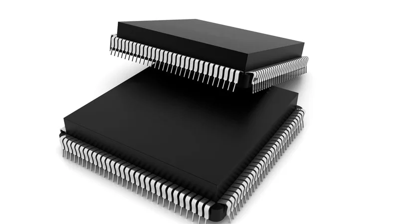
Packaged IC Chip
Introduction
Integrated circuit (IC) package types play a crucial role in electronics, offering protection and electrical connections for semiconductor devices such as transistors, capacitors, and other integrated circuit types. With technology advancing rapidly, many IC package types have emerged, each presenting distinct characteristics and advantages. Engineers and designers must grasp these differences to choose the most appropriate IC package types for their applications.
Among the commonly used IC package types are DIP, SOP, QFP, and BGA, each boasting its own set of characteristics, advantages, limitations, and applications. DIP stands out for its simplicity and cost-effectiveness, SOP excels in space efficiency, QFP offers a high pin count, while BGA is known for its enhanced electrical performance and superior thermal management capabilities.
IC Package Fundamentals
Integrated circuit (IC) packaging represents the culmination of a semiconductor's journey, serving as a crucial shield against environmental threats like dust, moisture, and corrosion for the delicate silicon die. Beyond protection, this robust casing facilitates essential electrical connections, enabling the IC to interact with the external world through a device's printed circuit board (PCB).
The evolution of IC packaging has been driven by a quest for miniaturization, performance enhancement, and increased functionality. The 1970s marked a significant advancement with the introduction of ball grid array (BGA) packages, offering substantial improvements over previous designs. As the 21st century began, innovative packaging technologies such as the plastic quad flat pack (PQFP) and the thin small outline package (TSOP) emerged, surpassing the limitations of traditional pin grid arrays (PGA).
The drive for miniaturization continued with the advent of land grid array (LGA) packages, notably championed by companies like Intel, offering a more compact design compared to BGAs. However, the evolution persisted, leading to the prominence of flip-chip ball grid arrays (FCBGAs), which surpassed BGAs in pin count capability.
Unlike traditional BGAs, where connections are limited to the edges of the die, FCBGAs distribute input and output signals across the entire die surface. This design enhancement significantly enhances the functionality and versatility of modern electronic devices.
Understanding the ongoing development of IC packaging provides insights into the intricate balance between miniaturization, performance enhancement, and protection that defines modern electronics.
Recommended reading: What is a Semiconductor? A Comprehensive Guide to Engineering Principles and Applications
The Building Blocks of IC Packages
Beneath the protective exterior lies a complex network of critical elements within an IC package, each fulfilling a pivotal role in the IC's operation. Here's a detailed breakdown of these fundamental components:
Die: At the core of the IC lies the die, a minute silicon chip housing the intricate circuitry responsible for the device's specific functions.
Leadframe: Composed of thin metal, typically copper or alloy steel, the leadframe serves dual roles:
Electrical Connections: The leadframe provides external connection points (pins) for the device.
Mechanical Support: It forms a robust foundation for the die.
Substrate: Serving as the foundation for mounting the die and other components, the substrate facilitates:
Electrical Connections: The substrate enables connections between the die and the external pins.
Mechanical Support: It provides additional stability for the entire package. Substrates can be crafted from various materials such as ceramic, organic materials, or a blend of both.
Wire Bonds: These microscopic wires, often made of gold or aluminum, create the electrical link between the die and the leadframe or substrate, acting as minute conduits for signals between the internal circuitry and the external pins.
Encapsulant: A protective molding compound, typically epoxy resin, that encloses and safeguards the entire assembly (die, leadframe, wires, and substrate). It offers several benefits:
Mechanical Strength: The encapsulant provides structural integrity to the package.
Environmental Protection: It shields the components from contaminants like dust and moisture.
Thermal Management: Some encapsulants aid in heat dissipation.
Materials and Selection Considerations
The selection of materials for IC packages is a critical consideration, tailored to meet the specific demands of the application. Common materials include:
Leadframe: Copper, copper alloys, or iron-nickel alloys strike a balance between conductivity and mechanical strength.
Substrate: Laminates (FR-4, BT) offer cost-effectiveness, ceramics (alumina, aluminum nitride) provide high thermal conductivity, and TAB materials offer flexibility.
Wire Bonds: Gold boasts superior conductivity but is costly, while copper provides a good compromise, and aluminum is a cost-effective option.
Encapsulant: Epoxy molding compounds are favored for affordability and ease of use, while ceramics offer superior thermal performance and resins cater to specific applications.
Common IC Package Types
There are many IC packages and different ways of classifying them. On the subject of IC packages, it is common to come across technical abbreviated terms such as DIP, SIP, SOP, SSOP, TSOP, MSOP, QSOP, SOIC, QFP, TQFP, BGA, etc. These are all names of different IC packages and they can be categorized in different ways.
IC package types can be distinguished by their mounting style, as they fall into two broad categories, namely Through-hole and Surface Mount Technology (SMT). Through-hole packages have their leads inserted through holes on the PCB and then soldered, while surface-mount packages have components mounted directly on the exterior of the board. Surface mount packaging components are called surface mount devices (SMD).
Another way to classify IC packages is by their pin layout. Integrated circuits are usually linear, square, or rectangular shaped, so the pin layout can be linear, in two parallel directions, on the four sides, or in matrix form. Further classification can be done by pin or terminal shape.
The shapes can be linear, L-shape, J-shape, needle shape, mutual folding, and tape/film shape, among others. Lastly, IC packages can be distinguished by terminal or pin count. There are two-terminal, three-terminal, four-terminal, five-terminal, six-terminal, and over six-terminal packages. The terminal dimensions may also serve as a differentiating factor for similar package types.
Recommended reading: SMT Assembly vs. Through-Hole: What to Know
Some common types of integrated circuit packaging are discussed in the subsequent sections.
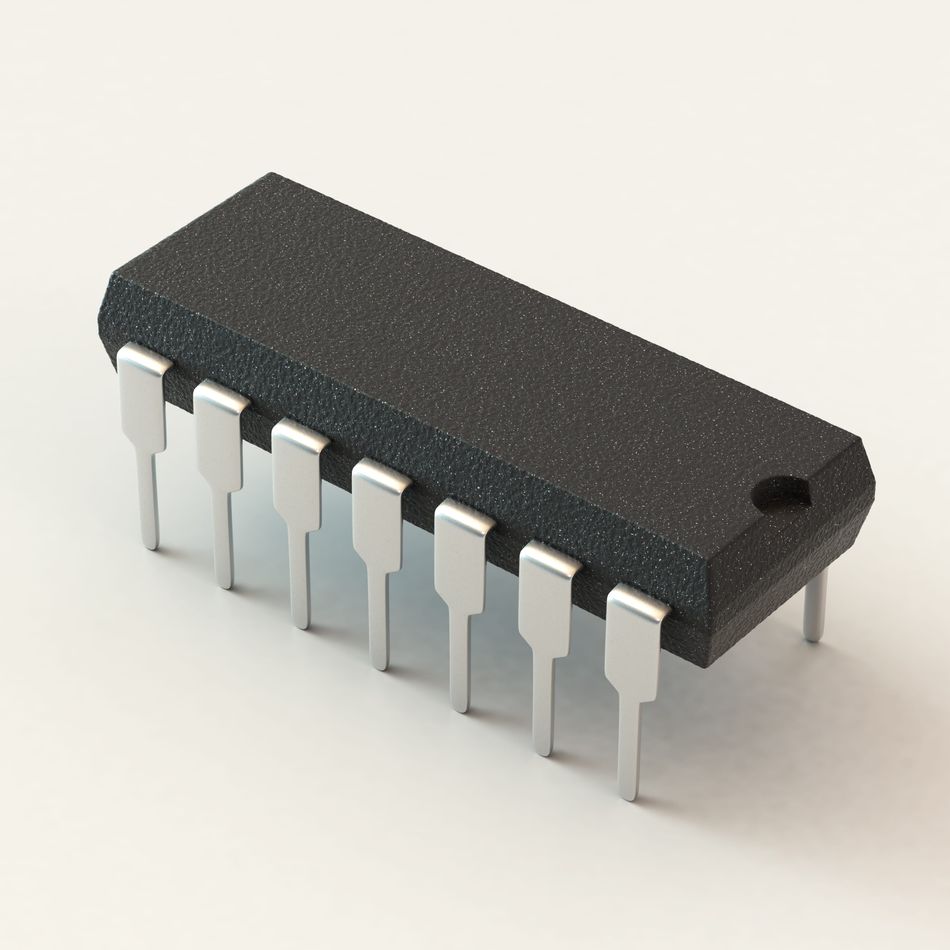
1. Dual In-line Package (DIP)
These iconic packages are the seasoned warriors of the electronics world. Easily recognizable by their rectangular shape with two parallel rows of metal legs for through-hole mounting, DIPs were once the go-to choice. Their simplicity and ease of use made them perfect for hobbyists and early electronic devices. However, their larger footprint makes them less suitable for the miniaturization demands of modern electronics.
Benefits of DIP packages:
Easy manual handling and insertion into PCBs
Suitable for low-density, low-frequency applications
Sturdy mechanical connection to the PCB
Allows for easy replacement and servicing
Drawbacks of DIP packages:
Larger footprint compared to surface-mount packages
Limited pin count capacity
Higher lead inductance and capacitance, affecting high-frequency performance
Not suitable for high-density PCB designs
Common applications for DIP packages:
Through-hole PCB assemblies
Low-frequency analog and digital circuits
Prototype and hobbyist projects
Legacy systems and replacements for older components
Technical specifications and package dimensions:
Package dimensions: 6 mm x 4 mm to 64 mm x 14 mm
Pin count: 8 to 64 pins
Lead pitch: 2.54 mm (0.1 inches)
Lead length: 3 mm to 4 mm
Package height: 3 mm to 5 mm
2. SOP (Small Outline Package) & QFP (Quad Flat Package)
As technology advanced and devices shrunk, so did the IC packages. SOPs and QFPs are the surface-mount champions, designed for direct soldering onto the printed circuit board (PCB) surface. SOPs offer a smaller footprint compared to DIPs, with leads extending from two sides of the package. QFPs take miniaturization a step further, featuring leads on all four sides, enabling a higher pin count for complex ICs. This makes them ideal for a wide range of modern applications.
QFP package variations:
Low-profile Quad Flat Package (LQFP): Thinner version with reduced package height
Thin Quad Flat Package (TQFP): Even thinner, with a package height of 1 mm or less
Plastic Quad Flat Pack (PQFP): QFP with plastic encapsulation material
Ceramic Quad Flat Pack (CQFP): QFP with ceramic encapsulation material
Benefits of QFP packages:
Higher pin count capacity than DIP packages
Smaller footprint for higher-density PCB designs
Suitable for surface-mount technology (SMT) assembly
Good thermal performance due to exposed leads on all sides
Drawbacks of QFP packages:
More challenging to handle and solder than DIP packages
Requires specialized SMT assembly equipment and processes
Higher cost compared to DIP packages
Limited heat dissipation compared to packages with exposed pads or heat spreaders
Common applications for QFP packages:
Microcontrollers and digital signal processors
Automotive electronics
Consumer electronics (smartphones, tablets)
Technical specifications and package dimensions:
Package dimensions: 4 mm x 4 mm to 40 mm x 40 mm
Pin count: 32 to 256 pins
Lead pitch: 0.4 mm to 1.0 mm
Package height: 1 mm to 3 mm
Lead length: 0.5 mm to 1.5 mm
3. Ball Grid Array (BGA)
When it comes to pushing the boundaries of miniaturization and performance, BGAs reign supreme. These advanced packages ditch the traditional leads altogether, opting for an array of solder balls on the underside. This design allows for a significantly smaller footprint while accommodating a high pin count, making them perfect for high-powered devices like microprocessors, FPGAs, ASICs, and graphics cards. However, their intricate design necessitates specialized assembly techniques and equipment.
Unique features of BGA packages:
Grid array of solder balls for electrical connections
No leads extending from the package sides
Solder balls are directly attached to the PCB pads
Allows for a high pin count in a small package footprint
Benefits of BGA packages:
High pin count capacity, often exceeding 1000 pins
Small package footprint, enabling high-density PCB designs
Excellent electrical performance due to short interconnect lengths
Good thermal performance, as the solder balls provide a direct thermal path to the PCB
Suitable for high-speed and high-frequency applications
Drawbacks of BGA packages:
BGA's hidden connections make visual inspection for defects tricky.
Reworking faulty BGAs is more challenging due to the delicate solder ball connections.
The reliance on solder balls makes BGAs more prone to stress-related failures.
BGA's high pin count and complex assembly often lead to higher manufacturing costs
Common applications for BGA packages:
High-performance microprocessors and graphics processing units (GPUs)
Field-programmable gate arrays (FPGAs) and complex programmable logic devices (CPLDs)
Application-specific integrated circuits (ASICs)
Memory devices, such as DDR SDRAM and NAND flash
High-speed communication interfaces, such as Ethernet and PCI Express
Technical specifications and package dimensions for BGA packages:
Package dimensions: Typically range from 5 mm x 5 mm to 50 mm x 50 mm
Ball count: Typically ranges from 100 to over 1000 balls
Ball pitch: Typically ranges from 0.5 mm to 1.27 mm
Package height: Typically ranges from 1 mm to 2.5 mm
Ball diameter: Typically ranges from 0.25 mm to 0.6 mm
4. Chip Scale Package (CSP)
A small, lightweight package with dimensions similar to the die size, offering a high-density interconnect solution with a small footprint. CSPs are often used in space-constrained applications, such as mobile devices and wearables.
Key characteristics of CSP packages:
Package size: Typically 1.2 times the die size or smaller
Thin profile: Package height of 1 mm or less
High-density interconnect: Fine pitch between contacts
Reduced package parasitics: Improved electrical performance
Benefits of CSP packages:
Miniaturization: Enables the development of smaller, more compact electronic devices
Improved electrical performance: Shorter interconnects reduce signal delays and improve signal integrity
Enhanced thermal performance: Small package size allows for better heat dissipation
Lower cost: Less material and simpler manufacturing process compared to larger packages
Increased reliability: Small size and fewer interconnects reduce the risk of package-related failures
Drawbacks of CSP packages:
Small size and hidden connections in CSPs make visual inspection for defects a challenge.
Delicate solder connections in CSPs complicate rework (replacing a faulty component).
CSPs can struggle with heat dissipation due to the proximity of the die to the package.
Applications where CSP packages are preferred:
Mobile devices: Smartphones, tablets, and wearables
Internet of Things (IoT) devices and sensors
High-density memory modules
Miniaturized medical devices and implantables
Space-constrained electronic systems: Smartcards and RFID tags
Technical specifications and package dimensions:
Package dimensions: 2 mm x 2 mm to 10 mm x 10 mm
Package height: 1 mm or less
Pitch between contacts: 0.4 mm to 0.8 mm
Number of I/O contacts: 16 to 200
Die size to package size ratio: 1.2 or smaller
Package Type | Size Range (mm) | Pin Count Range | Pitch (mm) | Thermal Performance |
DIP | 6 x 4 to 64 x 14 | 8 to 64 | 2.54 | Low |
QFP | 4 x 4 to 40 x 40 | 32 to 256 | 0.4 to 1.0 | Moderate |
BGA | 5 x 5 to 50 x 50 | 100 to 1000+ | 0.5 to 1.27 | High |
CSP | 2 x 2 to 10 x 10 | 16 to 200 | 0.4 to 0.8 | High |
Factors Influencing Package Selection
Choosing the appropriate IC package for a given application involves considering several technical factors that impact the overall performance, reliability, and cost of the system. These factors include:
Performance requirements:
The package must meet the desired electrical performance, such as signal integrity, power integrity, and thermal management.
High-speed applications may require packages with low inductance and capacitance to minimize signal distortion and delay.
Signal integrity:
The package should provide adequate shielding and isolation to minimize crosstalk and electromagnetic interference (EMI).
Proper impedance matching and controlled impedance routing are essential to maintain signal integrity.
Power dissipation:
The package must efficiently dissipate heat generated by the IC to prevent thermal damage and ensure reliable operation.
Packages with exposed pads, heat spreaders, or heat sinks may be necessary for high-power applications.
High-frequency performance:
For applications operating at high frequencies (e.g., RF and microwave), the package must have low parasitics and minimal signal loss.
Specialized packages, such as cavity packages or air cavity packages, may be required to achieve the desired high-frequency performance.
Cost:
The package cost should be balanced against the required performance and reliability.
Factors such as package material, manufacturing process, and volume pricing can significantly impact the overall cost.
Manufacturing constraints:
The package must be compatible with the available manufacturing processes and equipment.
Considerations such as package size, lead pitch, and assembly requirements should be taken into account to ensure manufacturability.
The choice of IC package has a significant impact on circuit design and layout considerations. The package selection influences:
PCB layout: The package footprint, pin arrangement, and routing requirements must be considered when designing the PCB layout.
Signal routing: The package pin assignment and internal routing can affect the signal integrity and the ease of PCB routing.
Thermal management: The package's thermal characteristics dictate the heat dissipation requirements and the need for additional cooling solutions.
EMI/EMC: The package shielding and grounding features impact the electromagnetic compatibility (EMC) and the need for additional EMI suppression measures.
Careful consideration of these factors and their impact on circuit design and layout is crucial to selecting the most suitable IC package for a given application. Trade-offs may be necessary to balance performance, cost, and manufacturing constraints while ensuring the overall system reliability and functionality.
Package-Specific Design Considerations
When designing electronic systems, it is essential to consider the specific design requirements and constraints associated with each IC package type. This section discusses the key design considerations for common package types, including thermal management techniques, signal routing strategies, and package-specific layout rules.
Package Type | Thermal Management | Signal Routing | Layout Rules |
DIP | - Use wider traces and copper pours on the PCB to improve heat dissipation. - Provide adequate spacing between components to allow for air circulation. - Consider using heat sinks or thermal adhesives for high-power DIPs. | - Keep signal traces as short as possible to minimize inductance and capacitance. - Avoid routing signals near the edges of the package to reduce crosstalk. - Use ground planes to provide shielding and reduce EMI. | - Ensure proper clearance between pins and traces to avoid short circuits. - Follow the recommended hole size and pad dimensions for through-hole mounting. - Provide adequate space for manual soldering and inspection. |
QFP | - Use thermal vias to conduct heat from the package to the PCB ground plane. - Incorporate thermal pads or exposed pads to enhance heat dissipation. - Consider using thermal interface materials (TIMs) between the package and heat sink. | - Use controlled impedance traces to maintain signal integrity. - Minimize the trace length and avoid sharp bends to reduce reflections. - Implement differential pair routing for high-speed signals. | - Follow the recommended pad size and pitch for the specific QFP package. - Provide sufficient clearance between pads to avoid solder bridging. - Use via-in-pad or dog-bone structures for dense pin arrangements. |
BGA | - Implement thermal vias under the BGA package to conduct heat to the PCB layers. - Use thermal balls or thermal pads to enhance heat transfer from the package to the PCB. - Consider using heat spreaders or heat sinks for high-power BGAs. | - Use controlled impedance traces and maintain consistent trace widths and spacing. - Implement power and ground planes to provide low-impedance supply and return paths. - Use via shielding and ground shielding to reduce crosstalk and EMI. | - Follow the recommended ball pitch and pad size for the specific BGA package. - Implement proper via design and placement to ensure reliable connections. - Use solder mask-defined (SMD) or non-solder mask-defined (NSMD) pads based on the manufacturing process. |
CSP | - Use thermal vias to transfer heat from the package to the PCB layers. - Implement thermal pads or exposed pads to improve heat dissipation. - Consider using underfill material to enhance thermal conductivity and mechanical stability. | - Use fine-pitch traces and high-density interconnects (HDI) for routing. - Implement controlled impedance traces and maintain consistent trace geometry. - Use ground planes and shielding to minimize crosstalk and EMI. | - Follow the recommended pad size and pitch for the specific CSP package. - Use micro vias or blind vias for high-density interconnects. - Implement proper via design and placement to ensure reliable connections. |
When designing with specific IC packages, it is crucial to refer to the manufacturer's guidelines, application notes, and reference designs to ensure compliance with package-specific requirements. Proper consideration of thermal management, signal integrity, and layout rules is essential to achieve optimal performance, reliability, and manufacturability of the electronic system.
Recommended reading: Simulation accelerates the development of Photonic Integrated Circuits for automotive applications
Challenges and Limitations
IC packages offer numerous benefits but also present technical challenges and limitations that must be addressed during design and manufacturing. This section discusses key challenges and limitations associated with different IC package types and provides potential solutions or mitigation strategies.
Package-Induced Stress
Challenge: Mechanical stress on the die due to differences in thermal expansion coefficients between package materials and silicon die, leading to die cracking, delamination, or performance degradation.
Solution: Use low-stress packaging materials (low-CTE substrates and encapsulants) and implement stress-relief features (underfill materials or compliant interconnects) to absorb stress and protect the die.
Thermal Dissipation Limits
Challenge: Increased power densities make managing heat generated by the device more challenging, leading to overheating, reduced performance, and reliability issues.
Solution: Employ advanced thermal management techniques (thermal vias, heat spreaders, or heat sinks) and use high-thermal-conductivity materials (copper or aluminum nitride) for the package substrate and heat spreader.
Signal Integrity Issues
Challenge: High-speed and high-frequency signals suffer from crosstalk, reflections, and EMI due to package parasitics and interconnect characteristics.
Solution: Implement controlled impedance design techniques (trace width and spacing control), use ground planes and shielding, and employ advanced packaging technologies (flip-chip or wafer-level packaging) to minimize package parasitics.
Manufacturing Complexity
Challenge: Advanced IC packages (BGAs, CSPs, wafer-level packages) require precise manufacturing processes and tight tolerances, leading to increased costs, lower yields, and potential reliability issues.
Solution: Collaborate with packaging and assembly vendors to ensure proper design for manufacturability (DFM) guidelines, use design automation tools to optimize package layout, and implement robust quality control and testing procedures.
Electrical Performance Limitations
Challenge: IC packages introduce electrical limitations (increased resistance, inductance, capacitance) that impact device performance, power efficiency, and signal integrity.
Solution: Use low-resistance materials (copper or gold) for package interconnects and bumps, minimize interconnect lengths, optimize package layout, and employ advanced packaging technologies (2.5D or 3D packaging) for shorter interconnects and improved electrical performance.
Cost Considerations
Challenge: Due to increased complexity and specialized manufacturing processes, advanced IC packaging technologies (flip-chip BGAs, wafer-level packages) can be more expensive than traditional packaging methods.
Solution: Conduct a thorough cost-benefit analysis to determine the most suitable packaging technology for the specific application and volume requirements, explore alternative packaging options (QFN or LGA) that balance performance and cost, and optimize package design to minimize size and layer count.
Conclusion
Understanding IC package types is crucial for effective electronic design, as the choice of the package can significantly impact the performance, reliability, and cost of the final product. Engineers and designers must carefully consider technical factors, such as performance requirements, signal integrity, power dissipation, and manufacturing constraints when selecting an IC package for their projects. By taking into account package-specific design considerations, such as thermal management, signal routing, and layout rules, designers can optimize their designs and ensure the best possible performance and reliability.
As the electronics industry continues to evolve and demand more advanced and compact solutions, staying up-to-date with the latest IC packaging technologies and trends is essential. By leveraging the information provided in this article and considering the technical factors and design considerations, engineers and designers can make informed decisions when selecting IC packages for their projects and developing high-performance, reliable electronic systems.
Frequently Asked Questions (FAQs)
Q1: What are the main differences between through-hole and surface-mount IC packages? A1: Through-hole IC packages, such as DIP, have leads that are inserted into holes drilled in the PCB and soldered on the opposite side. Surface-mount packages, like QFP and BGA, have leads or pads that are soldered directly onto the surface of the PCB. Surface-mount packages offer smaller footprints, higher pin counts, and better high-frequency performance compared to through-hole packages.
Q2: How does the package type affect the thermal performance of an IC? A2: The package type plays a significant role in the thermal performance of an IC. Packages with exposed pads, such as QFP and BGA, provide a direct thermal path from the die to the PCB, allowing for better heat dissipation. Packages with a larger surface area, like BGA and CSP, also offer improved thermal performance compared to smaller packages. Additionally, the use of thermal vias, heat spreaders, and heat sinks can further enhance the thermal performance of an IC package.
Q3: What are the advantages of using BGA packages over QFP packages? A3: BGA packages offer several advantages over QFP packages, including higher pin counts, smaller footprints, and better electrical and thermal performance. The grid array of solder balls in a BGA package provides a shorter and more direct path between the die and the PCB, reducing inductance and improving signal integrity. BGA packages also allow for better heat dissipation due to the large number of thermal balls and the ability to use thermal vias under the package.
Q4: What is the purpose of underfill material in flip-chip and CSP packages? A4: Underfill material, typically an epoxy-based compound, is used in flip-chip and CSP packages to fill the gap between the die and the substrate. The primary purposes of underfill are to provide mechanical support, reduce stress on the solder bumps, and improve thermal conductivity. Underfill helps to distribute the stress caused by the difference in thermal expansion coefficients between the die and the substrate, preventing solder bump fatigue and cracking. It also enhances the thermal performance by providing an additional path for heat dissipation.
Q5: What are the challenges associated with designing high-speed circuits using BGA packages? A5: Designing high-speed circuits using BGA packages presents several challenges, including signal integrity, power integrity, and thermal management. The dense array of solder balls in a BGA package can lead to increased crosstalk and signal reflections, requiring careful signal routing and impedance matching. Power distribution in a BGA package must also be optimized to minimize voltage drops and ensure stable power delivery to the die. Additionally, the high power density of high-speed ICs in BGA packages necessitates efficient thermal management techniques, such as the use of thermal vias, heat spreaders, and heat sinks, to prevent overheating and ensure reliable operation.
Q6: What are the key considerations when selecting an IC package for a specific application? A6: When selecting an IC package for a specific application, engineers and designers must consider several key factors, including:
Performance requirements: The package must meet the electrical, thermal, and mechanical performance requirements of the application.
Size constraints: The package footprint and height must fit within the available space in the end product.
Pin count: The package must provide sufficient pin count to accommodate the IC's input/output and power requirements.
Cost: The package cost should be balanced against the performance and reliability requirements of the application.
Manufacturing compatibility: The package must be compatible with the available PCB assembly processes and equipment.
Reliability: The package must provide adequate protection against environmental factors, such as moisture, shock, and vibration, to ensure reliable operation over the product's lifetime.
By carefully evaluating these factors and considering the trade-offs between performance, cost, and manufacturability, engineers and designers can select the most suitable IC package for their specific application.
Reference:
Ebics. What is Packaged IC and Why is it Important? 2022. Available from: https://ebics.net/packaged-ic/ [Accessed: April 8, 2024].
Cadence Design Systems, Inc., "IC Packaging types," https://www.cadence.com/en_US/home/tools/ic-package-design-and-analysis.html [Accessed: April 8, 2024].
Engineers Garage. What are the Different Types of IC Packages? 2022. Available from: https://www.engineersgarage.com/ic-packages-types/ [Accessed: April 8, 2024].
R. R. Tummala, "Microelectronics Packaging Handbook," 3rd ed., Springer International Publishing, 2006.
Sierra Assembly. Types of Surface Mount Device Packages. 2021. Available from: https://www.sierraassembly.com/blog/what-are-the-popular-types-of-surface-mount-device-packages/ [Accessed: April 9, 2024].
RAYMING PCB & ASSEMBLY. LGA, PGA, BGA: What's the Difference Between the Grid Arrays? 2021. Available from: https://www.raypcb.com/lga-pga-bga/ [Accessed: April 9, 2024].