SMT Manufacturing: Everything You Need to Know
SMT stands for Surface-mount Technology, a method of soldering components directly onto a PCB. This article delves into the concept of SMT and the manufacturing process, as well as the benefits, drawbacks, and related terms.

14 Jun, 2022. 7 minutes read
SMT: Electronic production
Introduction
Surface mount technology (SMT) is an aspect of electronic assembly where electronic components, also called surface mount devices (SMD), are directly mounted onto the surface of a printed circuit board (PCB). Because of its cost and quality efficiency, SMT has become highly sought after in the industry.
What is Surface Mount Technology (SMT)?
Surface mount technology (SMT) is an assembly and production method that applies electronic components directly onto the surface of a printed circuit board (PCB). This process allows for automated production to complete more of the required assembly to create a working board. Any electrical component mounted in this manner is referred to as a surface-mount device (SMD). Unlike conventional assembly, SMT does not require components to be inserted through holes, rather components are soldered onto the board directly through reflow soldering.
Initially called Planar Mounting, SMT was first developed and applied by IBM to build small-scale computers in the 1960s, thereby becoming a replacement for its predecessor, Through-Hole Technology. However, it did not take off until 1986 when surface-mounted components managed to reach 10% market popularity. By 1990, surface-mounted devices or SMDs could be found in the majority of all high-tech printed circuit assemblies (PCAs).[1]
SMT components were designed to have small tabs where solder could be applied to attach SMDs to the surface of the PCB. In the era of Through-Hole Technology, components were mounted through lead holes that were drilled into PCBs. The holes were sized to fit each component to hold each piece tightly, then the grip was soldered. With SMT, the hole drilling step is bypassed as SMDs are quickly sorted and attached to the top of the PCB with little to no hole leads; thereby significantly cutting the process of device assembly.
The SMT assembly process can be tedious and time-consuming if done manually, due to the precision it requires to create high-quality surface mount assembly (SMA). So for better efficiency, most SMT manufacturing is done through automated assembly machines, especially when production is large scale.[2]
SMT components are significantly smaller than through-hole components, which makes for the production of sleek and attractive electronic devices suitable for modern times. Therefore these days, SMT is used in almost every electronic device ranging from toys to kitchen appliances, to laptops and smartphones.[3]
SMT Manufacturing Process
The SMT manufacturing process is broadly grouped into 3 stages, namely: solder paste printing, components placement, and reflow soldering. However, due to the demands of the SMT production process, these stages are further analyzed in the following outline:
1. SMC and PCB Preparation
This is the preliminary stage where the SMCs are selected and PCB designed. The board usually contains flat, commonly silver, tin-lead, or gold plated copper pads devoid of holes, called solder pads. Solder pads support the pins of the components like transistors and chips.
Another vital tool is the stencil, which is used to provide a fixed position for the next phase of the process (solder paste printing), according to the predetermined positions of solder pads on the PCB. These materials, along with others that are to be used in the manufacturing process must be properly examined for flaws.
2. Solder Paste Printing
This is a critical phase in the SMT process. During this phase, a printer applies solder paste using the prepared stencil and squeegee (a tool for cleaning in printing) at an angle ranging from 45° to 60°. Solder paste is a putty-like mixture of powdered metal solder and sticky flux. The flux serves as a temporary glue to hold the surface mount components in place as well as cleansing the soldering surfaces of impurities and oxidation.
The solder paste, on the other hand, is used to connect the SMC and solder pads on the PCB. It is pertinent that each pad is coated in the correct quantity of paste. Otherwise, there will be no connection established when the solder is melted in the reflow oven. In the electronics manufacturing industry, a reflow oven is an electronic heating device used in surface mount technology (SMT) to place electronic components on printed circuit boards (PCBs).
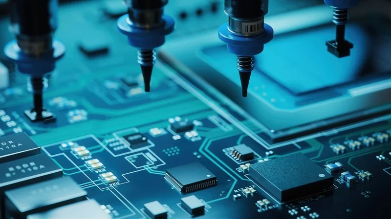
3. Components Placement
Next, pick-and-place machines are used to mount components on the PCB. Each component is removed from its packaging using a vacuum or a gripper nozzle, and the placement machine places it in its designed location. The PCB is carried on a conveyor belt while the electronic components are placed on it by the quick and accurate machines, some of which can place 80,000 individual components per hour.
Accuracy is required in this process because any erroneous placement soldered into a position can be costly and time-consuming to rework.
4. Reflow Soldering
After SMCs are placed, the PCB is then conveyed into the reflow soldering oven, where it passes through the following zones to undergo the soldering process:
Preheat zone: this is the first zone in the oven, where the temperature of the board and all the attached components is raised simultaneously and gradually. Temperature is cranked up at the rate of 1.0℃-2.0℃ per second until it enters 140℃-160℃.
Soak zone: here, the board will be kept at a temperature between 140℃ and 160℃ for 60-90 seconds.
Reflow zone: the boards then enter a zone where the temperature is ramped up at 1.0℃-2.0℃ per second to the maximum of 210℃-230℃ to melt the tin in the solder paste, welding the component leads to the pads on the PCB. While this is going on, the components are kept in place by the surface tension of the molten solder.
Cooling zone: this is the final section that ensures solder freezes upon exiting the heating zone to avoid joint defects.
If the printed circuit board is double-sided then these processes may be repeated using either solder paste or glue to hold the SMCs in place.
6. Cleaning and Inspection
After soldering, the board is cleaned and checked for flaws. If any is found, the defects are repaired and then the product is stored. Common ways used for SMT inspection include the use of magnifying lenses, AOI (Automated Optical Inspection), flying probe tester, X-ray inspection, etc. Instead of the naked eye, machines are used for quick and accurate results.
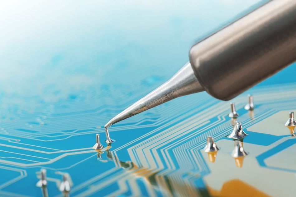
Soldering of PCB with electronic components
SMT: Pros and Cons
SMT has proven beneficial for PCB assembly (PCBA), PCB manufacturing, and electronics production in many ways including these:
Allows for smaller components
SMT process encourages increased automation
Maximum flexibility in building PCBs
Improved reliability and performance
Reduced manual intervention for component placement
Smaller, lighter boards
Ease of PCB assembly, using both sides of the board without the hole limitations that exist in the conventional method
Can co-exist with through-hole components, even on the same board
Increased density i.e more SMD components in the same space, or the same number of components in a much smaller frame
Low Cost of materials
Simplifies the production process and reduces the production cost. [4]
Conversely, disadvantages of SMT to electronic manufacturing include:
Small volume
Easily broken due to fragility
High requirements for soldering technology
Components can be easily dropped or damaged when installed.
It is not easy to use visual inspection, which is difficult to test.
Miniaturization and numerous solder joint types complicate the process and inspection.
Large investment in equipment such as the SMT machine
Technical complexity requires high training and learning costs.
Rapid development requires continuous follow-up. [5]
SMT vs SMD
SMT and SMD are frequently misunderstood and used simultaneously. Indeed, any technology and its actual components can be deeply entwined, creating confusion. Such is the case of SMT and SMD. This is why knowing the difference between an SMT assembly and individual SMD components is important.
In a simpler vein, SMT is the process in the technology, while SMD is the device involved in the technology. SMT is the technology that uses the method of directly placing and soldering electronic components on a PCB. These components are also sometimes called surface mount devices or SMDs. They are designed to be mounted on a printed circuit board (PCB).
SMDs make for devices produced faster, with more flexibility and less cost, without sacrificing functionality. They promise more functionality because smaller components allow for more circuits on small board space. This miniaturization is the major feature of SMD.[6]
Both SMT and SMD work together to provide users with faster, more energy-efficient, and more dependable PCBs.
Closing Thoughts
Smaller size, quicker production, and reduced weight are the major allures of SMT, leading to much easier electronic circuitry design and production, especially crucial in complex circuits. This higher level of automation has saved time and resources throughout the electronics manufacturing industry. As such, even though there is always a chance of developing new technology, SMT has undoubtedly secured its relevance.
References
SCRIBD. Surface-Mount Technology: History. 2019.[cited 2022 Jun 8]. Available from: https://www.scribd.com/document/106437192/SMD
Das S. SMT Machine and SMT Machine Manufacturers. 2021 [cited 2022 Jun 8]. Available from: http://www.electronicsandyou.com/smt-machine-and-smt-machine-manufacturers.html
Geospace Technology. SMT ASSEMBLY TECHNOLOGY: ALL YOU NEED TO KNOW. 2021.[cited 2022 Jun 9]. Available from: https://geospacemfg.com/blog/smt-assembly-technology/
Blog Industry News. Top Benefits of Surface-mount Technology (SMT) PCB Assembly. 2020. [cited 2022 Jun 9]. Available from: https://www.pcbnet.com/blog/benefits-surface-mount-technology-smt-pcb-assembly/
PCBWay. Advantages and Disadvantages of Surface Mounting Technology. 2019.[cited 2022 Jun 9]. Available from: https://www.pcbway.com/blog/PCB_Assembly/Advantages_and_Disadvantages_of_Surface_Mounting_Technology.html
6. History Computer (HC). Surface-Mount Technology. 2022. [cited 2022 Jun 9]. Available from: https://history-computer.com/smt-surface-mount-technology/