RF PCB: Design, Materials, and Manufacturing Processes
This article delves into the world of RF PCBs, exploring the design considerations that ensure signal integrity, the materials that minimize signal loss, and the intricate processes that bring these high-performance boards to life.

13 Mar, 2024. 15 minutes read
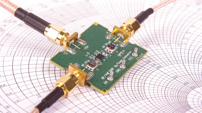
Amplifier Simulation in RF PCB
Introduction
RF PCB, or Radio Frequency Printed Circuit Board, refers to a specialized type of PCB designed to receive and transmit radio signals within a certain frequency range. These boards are the backbone of various modern electronics and communication systems, including mobile phones, radar systems, GPS devices, and wireless networks. Unlike their everyday counterparts, RF PCBs operate at high frequencies, demanding meticulous design, specific materials, and specialized manufacturing techniques.
This article delves into the world of RF PCBs, exploring the design considerations that ensure signal integrity, the materials that minimize signal loss, and the intricate processes that bring these high-performance boards to life. By understanding these aspects, we gain a deeper appreciation for the complexity and ingenuity behind the devices that connect us in a wireless world.
Understanding RF PCB
RF Circuit Boards are distinguished from standard PCBs by their ability to handle high-frequency signals, which can range from 500 MHz to 2 GHz and beyond. [1] This capability is critical in minimizing signal loss and ensuring signal integrity over a wide frequency range. RF PCB design and manufacturing demand precise control of dielectric constant and loss tangent for optimal high-frequency performance.
In high-speed RF PCBs, specific via types like blind vias and through-hole technology are used to minimize signal loss and maintain controlled impedance. Furthermore, the ground plane plays a crucial role in minimizing noise and ensuring a stable reference for RF traces.
The significance of frequency in RF PCB applications cannot be overstated. High-frequency signals are more susceptible to loss and require careful consideration of the PCB layout, material selection, and component placement to minimize signal attenuation and electromagnetic interference (EMI). The choice of substrate material, for instance, plays a pivotal role in determining the board's efficiency at transmitting RF signals. Materials with a low dielectric constant and loss tangent are preferred to reduce signal loss and support higher-frequency applications.
RF PCBs are crucial in modern technologies where wireless communication is essential. These include, but are not limited to, mobile communication devices, radar systems, GPS units, wireless networking equipment, and satellite communication systems. The ability of RF PCBs to efficiently manage high-frequency signals makes them indispensable in developing and operating these technologies.
Key Components of RF PCB
RF PCB usually consists of antennas, filters, and amplifiers, each with separate RF functions. Antennas are crucial for transmitting and receiving electromagnetic signals. Their design and placement on the PCB are critical factors that affect the overall system's range and efficiency. Filters play a vital role in selecting and isolating frequencies of interest, ensuring that the device operates within its designated frequency band while rejecting unwanted signals. Amplifiers, on the other hand, are used to increase the strength of weak signals, ensuring that they can be processed effectively without being drowned out by noise. [2]
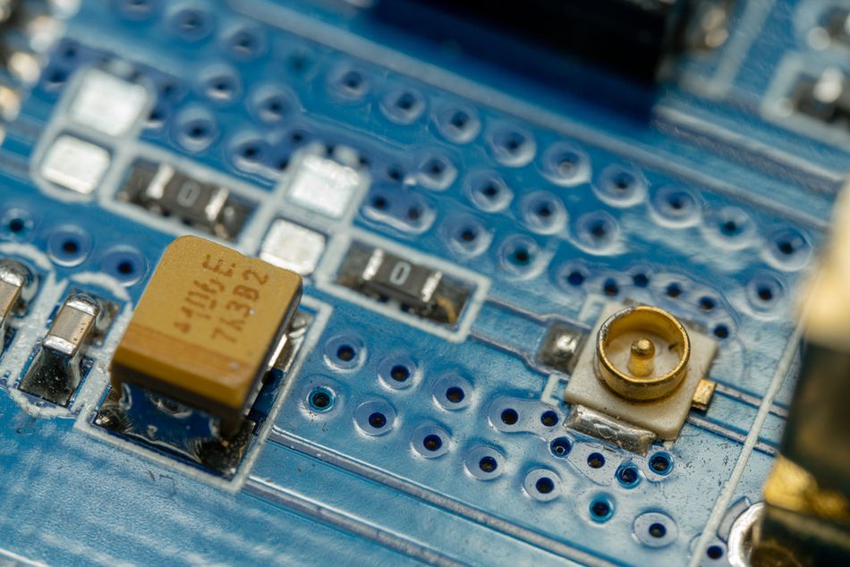
Each component within an RF PCB works to achieve the desired functionality. For example, in a wireless communication device, the antenna receives an incoming RF signal, which is then passed through a filter to isolate the signal of interest. The filtered signal may then be amplified to a suitable level for processing by the device's circuitry. This interplay of components is carefully engineered to optimize the performance of the RF system, taking into account factors such as signal strength, bandwidth, and interference.
The Science behind RF PCBs
Here's a closer look at the science behind RF PCBs:
Electromagnetic Wave Propagation: RF signals travel on the PCB traces as electromagnetic waves. These waves consist of an electric field and a magnetic field that propagate together. The design of the trace geometry, the dielectric material between layers, and the surrounding environment all influence how these waves propagate.
Signal Integrity: Maintaining a clean and undistorted signal is paramount in RF applications. Signal integrity refers to the ability of a signal to travel from its source to its destination on the PCB with minimal distortion or loss. Factors like impedance mismatch, crosstalk, and signal attenuation can severely degrade signal integrity.
Controlled Impedance: Impedance is the opposition a signal encounters as it travels along a conductor. In RF PCBs, maintaining a controlled impedance is crucial. Deviations from the desired impedance can cause signal reflections, leading to power loss and distorted data. Microstrip design involves careful consideration of trace width, substrate properties, and thickness to achieve the desired impedance.
High-Frequency Materials: Standard FR4 material, commonly used in everyday PCBs, becomes problematic at high frequencies. RF PCBs often utilize specialized substrates with lower dielectric constants to minimize signal loss. These materials, like PTFE (polytetrafluoroethylene), Rogers RT Duroid or Taconic, offer excellent electrical properties for high-frequency applications.
Signal Loss Mechanisms: Several mechanisms contribute to signal loss on RF PCBs at high frequencies. These include:
Conductor Loss: Due to the resistance of the copper trace itself, some signal power dissipates as heat.
Dielectric Loss: The dielectric material between layers also absorbs some signal energy.
Radiation Loss: A small portion of the signal energy can radiate away from the trace if not properly contained.
By understanding the scientific principles behind signal propagation, impedance control, and material properties, RF PCB designers can create high-performance boards that enable seamless wireless communication.
Materials Used in RF PCB
The fabrication of RF PCBs utilizes a variety of materials, each selected for its specific properties that cater to high-frequency applications. Common materials include FR4, Rogers materials, Teflon, Hydrocarbon resins, and Ceramic substrates.
FR4 is the standard material used in PCB manufacturing due to its cost-effectiveness and decent performance at lower frequencies. However, its high dielectric constant and loss tangent make it less suitable for high-frequency RF applications, as it can lead to significant signal loss and dispersion.
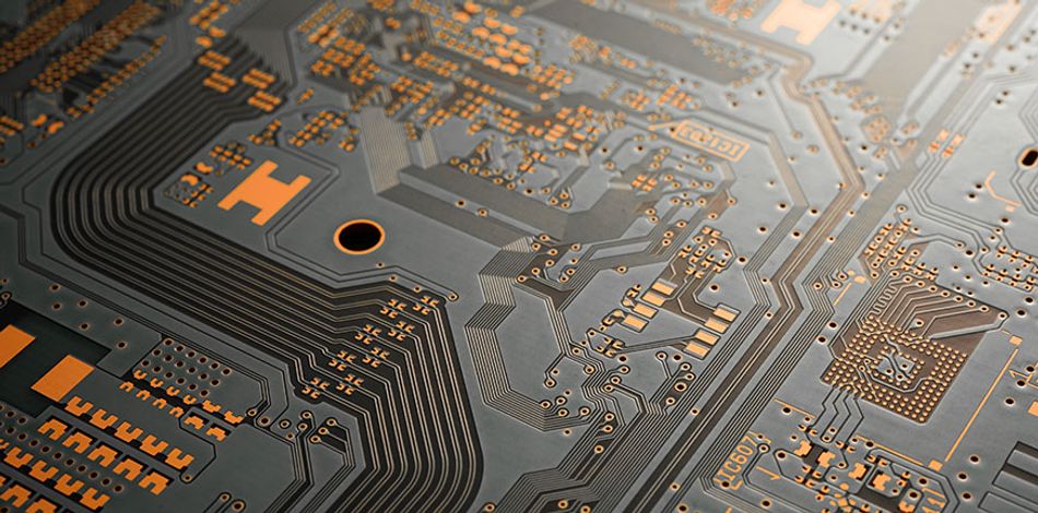
Rogers materials are a group of high-frequency laminates offering lower dielectric constants and loss tangents than FR4. These properties make Rogers materials an excellent choice for RF PCBs, as they can significantly reduce signal loss and support higher frequency ranges. Rogers materials exhibit low moisture absorption, contributing to their stable electrical properties under varying environmental conditions. [3]
Teflon, known for its extremely low dielectric constant and loss tangent, is another preferred RF PCB material, especially in applications requiring high frequencies. Teflon's outstanding electrical properties ensure minimal signal loss and phase shift, making it ideal for critical RF applications. However, Teflon's softness and high cost can pose challenges in PCB manufacturing and limit its use to specific high-performance applications.
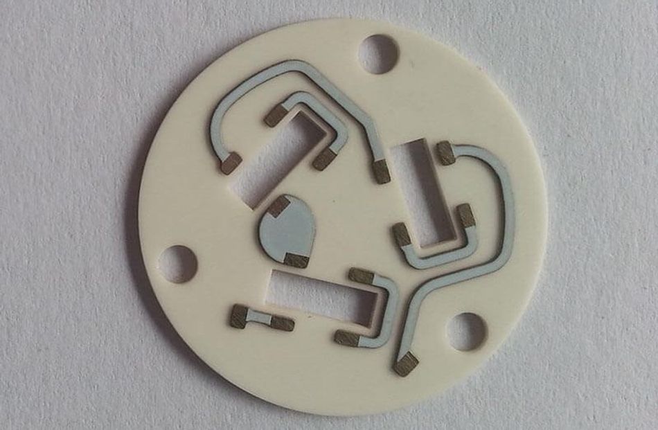
Ceramic substrates offer high thermal conductivity, excellent dielectric properties, and superior mechanical stability, making them suitable for high-power RF applications. Their ability to withstand high temperatures and maintain stable electrical properties under thermal stress is particularly beneficial in applications where heat dissipation is a concern.
The choice of material has significant performance implications in RF PCB design. While FR4 may be sufficient for lower frequency or less critical applications, the superior electrical properties of Rogers materials, Teflon, and Ceramic substrates make them more suitable for high-frequency, high-performance applications. PTFE has a high Coefficient of Thermal Expansion (CTE), so careful design considerations are needed when using it in RF PCBs. The decision between these materials involves a trade-off between cost, performance, and manufacturability for specific application needs.
Recommended Reading: What are Circuit Boards Made Of?
Design Considerations for RF PCB
Impedance matching is a critical aspect of RF PCB design. Mismatches can lead to signal reflections, which cause power loss and further degrade the system’s performance. PCB trace impedance should match the impedance of RF components, usually 50 or 75 ohms. [4] Achieving this requires precise calculations and adjustments to the trace width, dielectric constant of the substrate, and the thickness of the PCB.
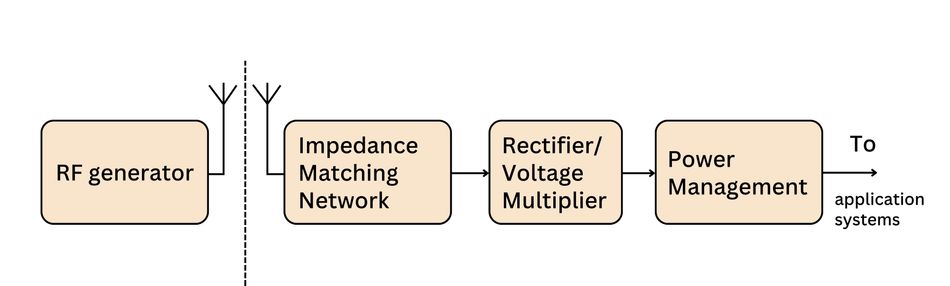
Designing for high frequencies introduces several challenges, such as signal loss and cross-talk. Signal loss occurs due to the inherent resistance of the materials and can be exacerbated by higher frequencies. This can cause the skin effect, where alternating current tends to flow on the surface of the conductor, increasing the effective resistance. Cross-talk is another concern, where a signal from one trace or component inadvertently couples with another, leading to interference and potential data corruption. This is particularly problematic in RF PCBs due to the high-frequency signals that can more easily couple between closely spaced conductors.
The layout and component placement on an RF PCB are also crucial for optimal performance. The placement of components must consider the signal path and minimize the distance high-frequency signals must travel to reduce the chance of loss and interference. Additionally, the layout must account for the isolation of sensitive components to prevent cross-talk and the creation of unintentional antennas that could radiate or pick up signals, leading to further interference.
Simulation and Modeling
Simulation and modeling tools are indispensable in designing RF PCBs. These tools, such as High-Frequency Structure Simulator (HFSS) and Advanced Design System (ADS), allow designers to create virtual circuit models and predict how they will behave before any physical prototypes are built. They can simulate electromagnetic fields and signal interactions within the PCB, providing insights into potential issues like impedance mismatches, signal integrity problems, and electromagnetic compatibility (EMC) concerns. [5]
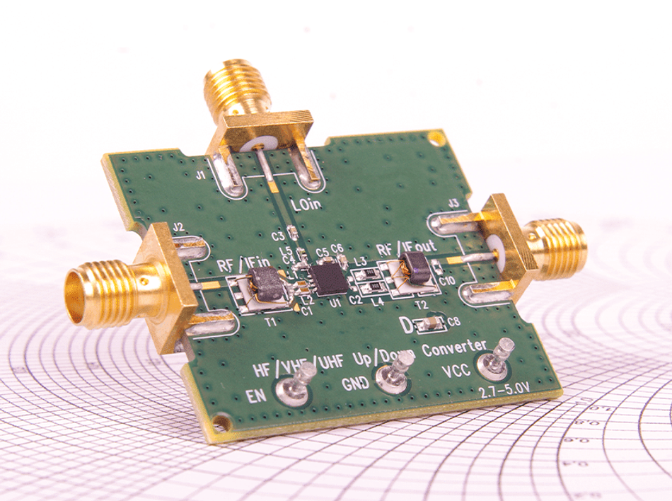
Simulation aids in predicting and mitigating design issues by allowing designers to test and refine their designs iteratively. For example, they can adjust trace widths and spacings, modify RF PCB stack-ups, and reposition components virtually to see how these changes affect impedance, signal loss, and cross-talk. This process helps optimize the design for performance before moving on to the manufacturing phase.
Parameters typically analyzed during simulation include S-parameters, which describe the signal behavior at RF and microwave frequencies, including reflection and transmission coefficients. Other parameters include voltage standing wave ratio (VSWR), which is a measure of characteristic impedance matching, and electromagnetic fields to assess the potential for radiation and susceptibility to external interference. By analyzing these design guidelines, engineers can make informed decisions to enhance the performance and reliability of the final RF PCB.
Prototyping and Testing
Prototyping an RF PCB is a multi-step process that begins with the creation of a detailed design, which is then used to manufacture a physical prototype. The initial step involves transferring the PCB layout onto a substrate, followed by etching away excess material to create the necessary traces and patterns. Components are then placed and soldered onto the board, either manually for simple prototypes or using automated processes for more complex designs. Once assembled, the prototype undergoes an initial inspection to check for manufacturing defects.
Common tests to evaluate RF performance include network analysis to measure S-parameters, which provide information on how the RF PCB responds to different frequencies. Time-domain reflectometry (TDR) tests are used to assess impedance uniformity and locate discontinuities or impedance mismatches. Shielding effectiveness tests may also be conducted to determine how well the PCB can protect against external electromagnetic interference. [6] Additionally, thermal testing is performed to ensure that the board operates reliably under the expected range of operating temperatures.
Iterative testing and refinement are crucial in the design process of RF PCBs. Initial tests on the prototype often reveal areas where performance can be improved, such as reducing signal loss or mitigating cross-talk. These findings lead to modifications in the design, such as adjusting trace widths or changing the layout to improve isolation between components. Subsequent prototypes are then produced and tested, repeating until the design meets all performance criteria. This iterative approach ensures that the final RF PCB design is as efficient and reliable as possible before it goes into mass production.
Recommended Reading: Mastering PCB Testing: Techniques, Methods, and Best Practices Unveiled
Manufacturing Processes
The fabrication process of RF PCB resembles standard PCB manufacturing but requires added precision and considerations for high-frequency applications. Initially, the process begins with the selection of suitable substrate materials that meet the required electrical properties for RF applications, such as low dielectric constant and loss tangent. The design is then transferred onto the substrate using photolithography, where a photoresist is applied and exposed to ultraviolet light through a mask, defining the pattern of the circuit. [7]
Precision in layer alignment and etching is paramount in RF PCB manufacturing due to the high frequencies at which these boards operate. Misalignment between the top layer and bottom layer can lead to impedance mismatches and signal integrity issues, significantly affecting the performance of the final product. Similarly, the etching process must be carefully controlled to ensure that the widths and spacings of the traces are accurate to the design specifications. Careful stackup design is critical for achieving the desired electrical performance and signal routing.
Soldering and assembly of RF components present unique challenges, primarily due to the sensitivity of these components to heat and the potential for signal degradation if not properly installed. Advanced soldering techniques, such as reflow soldering, are often employed to ensure a reliable connection while minimizing thermal stress on the components. In RF designs, the power supply interfaces need to be designed to minimize noise and ensure stable power delivery. Additionally, the placement of components must be meticulously planned to reduce the risk of cross-talk and electromagnetic interference, which can be more pronounced in RF PCBs due to the high-frequency signals involved.
Quality Control and Reliability
RF PCB manufacturing involves extensive inspection techniques, such as Automated Optical Inspection (AOI) and X-ray inspection, are utilized to detect any defects in the substrate, traces, and solder joints that could compromise the board's functionality. Electrical testing, including Time-Domain Reflectometry (TDR) for impedance characterization and network analysis for measuring S-parameters, is conducted to verify that the PCB performs as designed.
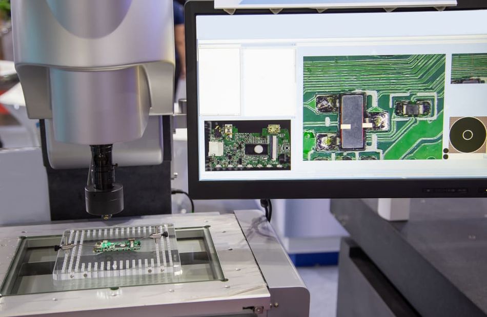
Reliability concerns specific to RF PCBs include issues related to signal integrity, such as phase noise, harmonic distortion, and intermodulation distortion. This can degrade the quality of the transmitted or received signals. To address these concerns, manufacturers implement design and fabrication practices that minimize sources of noise and interference. This includes the use of materials with stable electrical properties and designing layouts that optimize signal paths and shielding.
Common failure modes in RF PCBs, such as solder joint failures, trace delamination, and dielectric breakdown, are prevented through design optimization, material selection, and manufacturing controls. [8] For example, the use of high-temperature resistant substrates can reduce the risk of delamination, while careful control of the soldering process can prevent solder joint failures.
By adhering to these quality control measures, routing strategies and reliability practices, manufacturers can produce RF PCBs that meet the high standards required for today's advanced communication systems.
Recommended Reading: PCB Manufacture Process: A Comprehensive Guide to Understanding and Mastering the Techniques
Advanced Technologies in RF PCB
Emerging technologies and materials in RF PCB design and manufacturing are setting new benchmarks for performance and functionality. One of the significant advancements is the use of liquid crystal polymer (LCP) substrates, which offer exceptional electrical properties at high frequencies, including low dielectric constant and loss tangent, and high thermal stability. This material is particularly suited for applications in extremely high frequencies (EHF), including millimeter-wave (mmWave) technologies used in 5G communications and automotive radar systems.
Another notable advancement is the development of additive manufacturing techniques, such as 3D printing of RF circuits and components. This technology allows for the creation of complex, three-dimensional structures that were previously difficult or impossible to manufacture using traditional methods. The potential impact of these advancements includes reduced manufacturing costs, increased design flexibility, and the ability to produce small batches of customized RF PCBs efficiently.
Ongoing research in the field of RF PCBs is focused on further improving the performance and reducing the size of RF components and systems. This includes the development of new materials with even lower loss characteristics, as well as advanced design methodologies that optimize signal integrity and electromagnetic compatibility. Future trends are likely to include increased integration of RF functionality into multi-layer PCBs, enabling more compact and efficient designs for a wide range of applications.
Integration of Active and Passive Components
The trend towards integrating active and passive components directly onto the RF PCB is driven by the need for more compact, efficient, and cost-effective designs. This approach, known as integrated passive devices (IPD) or integrated passive and active components (IPAC), involves embedding components such as resistors, capacitors, inductors, and even transistors within the PCB substrate itself.
The benefits of this approach include reduced board size and weight, improved signal integrity due to shorter interconnects, and lower manufacturing costs by reducing the number of discrete components that need to be placed and soldered. Additionally, integration can enhance the performance of RF systems by minimizing parasitic effects and improving the overall electromagnetic compatibility of the device.
However, the integration of active and passive components presents several challenges, including the complexity of the manufacturing process and the need for specialized materials and equipment. Designers must also consider the thermal management of integrated components, as the embedded devices may generate heat that needs to be dissipated effectively.
Applications that benefit from integrated components include smartphones, wearable devices, and other compact electronic devices where space is at a premium. The integration of RF components into the PCB allows these devices to support a wide range of functionalities, including wireless communication, GPS, and Bluetooth connectivity, in a small form factor.
Flexible and Wearable RF PCBs
The development of flexible and wearable RF PCBs represents a significant advancement in the field of electronics, enabling the creation of devices that conform to various shapes and can be worn on the body. This flexibility is achieved through the use of materials such as polyimide or liquid crystal polymer (LCP), which offer both the necessary electrical properties for RF applications and the ability to bend or flex without breaking. These materials are combined with flexible conductive inks or thin metal films to create the conductive paths necessary for RF signal transmission.

Manufacturing techniques for flexible and wearable RF PCBs often involve roll-to-roll processes or laser ablation, which allow for the efficient production of large quantities of flexible circuits. The use of additive manufacturing, or 3D printing, is also emerging as a method to create custom, on-demand flexible RF PCBs for specific applications. These techniques must carefully balance the need for flexibility with the requirement to maintain the integrity of the RF signal paths, ensuring that bending or flexing does not significantly impact performance.
The applications and potential of flexible and wearable RF technologies are vast, ranging from smart clothing and wearable health monitors to flexible smartphones and foldable displays. In the medical field, flexible RF PCBs can be used to create wearable devices that monitor vital signs or deliver targeted therapies, providing continuous health monitoring without restricting the wearer's movement. In consumer electronics, the ability to integrate RF functionality into flexible substrates opens up new possibilities for innovative product designs that can adapt to the user's needs and preferences.
The development of flexible RF PCBs is constantly evolving. New materials and manufacturing processes are pushing the boundaries of what's possible. As these technologies mature, we can expect even more innovative and seamless wearable devices that integrate seamlessly with our lives. The future of wearable technology is undoubtedly flexible!
Recommended Reading: Beyond Rigidity: The Rise of Flexible Electronics
Conclusion
From the specialized materials required to minimize signal loss at high frequencies to the precise design considerations necessary for maintaining signal integrity, RF PCBs are a testament to the advanced engineering required for today's communication systems. The discussion has also touched upon the challenges and solutions in manufacturing, emphasizing the importance of precision and quality control to ensure reliable performance. Looking ahead, the future of RF PCB technology is poised to be shaped by emerging trends, such as the integration of active and passive components, the development of flexible and wearable PCBs. This also includes the continuous pursuit of materials and techniques that push the boundaries of what is possible in high-frequency applications.
FAQs
Q. What makes RF PCB design different from standard PCB design?
A. RF PCB design is distinct due to its focus on handling high-frequency signals, which requires careful consideration of materials, characteristic impedance matching, and layout to minimize signal loss and interference. Unlike standard PCBs, RF PCBs require meticulous routing strategies to ensure signal integrity in high-frequency applications.
Q. How do material choices impact the performance of an RF PCB?
A. Material choices are critical in RF PCBs as they directly affect the board's ability to transmit high-frequency signals. Materials with low dielectric constants and loss tangents are preferred to reduce signal loss and support higher frequency ranges.
Q. What are the challenges in RF PCB manufacturing, and how are they addressed?
A. Challenges in RF PCB manufacturing include maintaining precision in layer alignment and etching, as well as ensuring reliable soldering and assembly for RF components. These are addressed through advanced manufacturing techniques and rigorous quality control measures.
Q. How does the integration of components onto an RF PCB affect its functionality?
A. Integrating components onto an RF PCB can enhance functionality by reducing board size, improving signal integrity, and lowering manufacturing costs. However, it also introduces complexity in RF design and manufacturing.
Q. What are the emerging trends in RF PCB technology?
A. Emerging trends in RF PCB technology include the use of new materials like LCP, additive manufacturing, integration of active and passive components, and the development of flexible and wearable RF PCBs for a variety of applications.
Conclusion
[1] JHDPCB. How To Define High-Frequency PCB? [Cited 2024 March 12] Available at: Link
[2] Analog. RF Amplifiers [Cited 2024 March 12] Available at: Link
[3] Bayareacircuits. Rogers Material: Right for your next RF PCB? [Cited 2024 March 12] Available at: Link
[4] Circuitdigest. Understanding Impedance Matching in PCB Design with Example and Calculation [Cited 2024 March 12] Available at: Link
[5] CORE. Overview of Signal Integrity and EMC Design Technologies on PCB : Fundamentals and the Latest Progress [Cited 2024 March 12] Available at: Link
[6] Altium. EMI Shielding Techniques You Can Use in Your PCB [Cited 2024 March 12] Available at: Link
[7] ResearchGate. Development of Photolithography Process for Printed Circuit Board Using Liquid Crystal Mask in Place of Photomask [Cited 2024 March 12] Available at: Link
[8] Medium. What are the most common PCB failure modes and how can they be avoided? [Cited 2024 March 12] Available at: Link