The Printed Circuit Board Design and Manufacturing Cycle: Symbiotic Relationships Engage Innovation
Article 2 in our PCB design series: Collaboration between key players opens up space for innovation.

Last updated on 16 Nov, 2020. 7 minutes read
Introduction
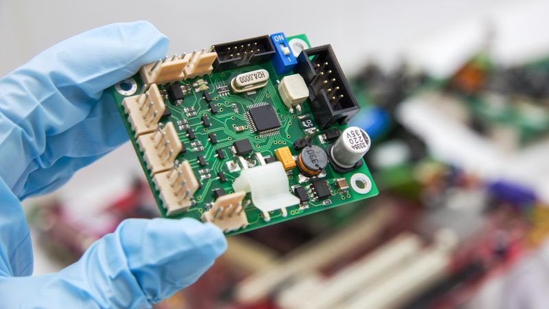
No matter the size of your electronic device, it’s going to have a Printed Circuit Board or PCB inside. These familiar green boards ensure our devices work the way they are intended. Their design, or the precise arrangement and choice of components, are at the heart of your device functionality. While a PCB is a ubiquitous object, the design cycle to bring it into existence is complicated, involving a huge number of stakeholders. The relationship between these key players greatly impacts the ability for innovation in the electrical systems and devices. This article will examine the design lifecycle of PCBs, introduce the key players in the design and manufacturing process, and highlight how collaborations within the design cycle can spur innovation.
PCB board design and manufacture is a multi-faceted process that converges multiple component manufacturers, designers, and processes. The scale of production can vary from a single engineer, designing, placing, and soldering their own board to multi-billion dollar manufacturing facilities printing millions of boards per year.
PCB designer
The functionality and quality of a PCB board starts with the decisions that a PCB designer or electrical engineer makes. Each board is embedded with a large variety of components. These range from resistors, capacitors, diodes, transistors, and fuses. Both the choice of the component, i.e., its individual capabilities and qualities plus their arrangement, and method and quality of fixing affect the overall size, quality, and function of the board. Either poor component choice or poor mapping of components can both lead to a lower quality PCB.
Designing a board has four major steps:
1. Parts research and selection
At this stage, the designer is looking to find the right selection of components to fulfill the function of the board. As comments or PCB parts are constantly getting upgraded and new products are being released, this stage requires careful research to select the most appropriate component for the board’s intent and budget. This research is done on a component manufacturer’s website or via an online component library.
2. Schematic capture and selection
The schematic capture is the general electrical layout of the board. This is usually done with a piece of CAD software known as a schematic editor. Once done, tests can be performed to check the integrity of circuit designs, and to compare the effects of components and signals upon the design. Simulations on the design at this stage can quickly identify the majority of bugs and errors before the design is physically manufactured. Adequate testing and simulation at this level significantly reduces the amount of time-to-market and production cost.
3. Board layout
Upon capturing the schematic and simulating the design, a physical prototype is built to test the board’s performance under real load conditions. At this stage, electronic design automation tools in a CAD program assist the designer in turning the board schematic into a ‘real-looking’ board by converting the symbols for components that represented the design in the capture stage into the physical dimensions of the represented components.
4. Verification and validation.
Prototype tests and manufacturing tests are the final steps in the validation of a PCB.
The final design is then exported to a Gerber format, which can be used by PCB manufacturers to create a physical representation of the board. A prototype test validates if the design meets the target specifications, while a manufacturing test ensures that high-volume production of the board is possible.
Component designers and manufacturers
Component manufacturers may specialize in specific industries or parts or create components across diverse portfolios. Manufacturers are the gatekeepers to innovation in some respects as they must continually find ways to improve on existing products to make them more efficient, safer, more powerful while adhering to miniaturization trends.
PCB assembly
PCB assembly usually occurs in a large manufacturing facility. These may specialize in printing boards at a large scale or have the capacity to create one-off or small-run designs. Parts of the process may involve automation and machinery while other aspects are still done with the dexterity, knowledge, and skill of PCB assemblers. There are a large number of steps involved to go from Gerber file to completed PCB. This video gives a concise overview:
PCB incorporation into the device
Physically adding the completed PCB into a device happens in the assembly of the overall product. This usually happens in a factory type environment and depending on the product may have elements completed using automation, or manually on a production line. By the time the PCB is ready for installing into its final home, it may have parts from several different countries, and input from designers in others.

How the PCB Design Process is evolving to boost innovation
Computer-Aided Design (CAD) came to the PCB industry in the late 80s becoming commonplace by the late 90s. This revolutionized a process that before was intensely manual and laborious. As CAD systems developed, it became the norm for PCBs to be designed as both 2D schematics and full 3D boards. This allowed for virtual testing and better quality control. However, it also replaced the arduous work of manually designing boards with the intense work of 3D modeling each and every component and board layout.
PCB design bureaus did begin to create CAD libraries of common components. Unlike architecture, where common CAD objects rarely change, PCB component manufacturers may launch hundreds of products a year - keeping on top of every single new release is a massive challenge. Not to mention having to create a new 3D model for every single new component for each design that it was to be included in. This began to change about a decade ago with the introduction of online component libraries that offered designers and engineers the chance to download pre-made models for their designs, both saving them huge amounts of time and helping them stay up to date on the latest available components.
SamacSys
One of the leading online CAD libraries is SamacSys. The component library tool allows engineers to download fully realized CAD models of PCB components directly into their drawings. The models don’t need to be unzipped or even imported. SamacSys works by pairing with major manufacturers to get their components modeled, checked then available in the library for engineers to use for free. This is not only a huge help to engineers working at all scales, but it provides the manufacturer with an insight into design trends much earlier than before. They can understand which components are popular for use and respond to this by increasing production or shifting design teams into that area.
Nexperia and SamacSys
Nexperia is one of the world leaders in semiconductor development and manufacture. We chatted with Edwin Van De Merbel from the European Nexperia marketing team to get an idea of how SamacSys fits into their vision to help make engineers more efficient.
Nexperia produces and sells up to 100 billion semiconductors annually, with products going into mobile phones, industrial applications, and consumer products. If you want to do electronic design, Nexperia is likely to have the products you need. We asked Edwin why Nexperia chooses to be a part of the SamacSys library. “We wanted to help our engineering customer community with additional design support,” explains Edwin. “We are continuously looking for ways to make the life of an electronics designer as easy as possible.”
Before services like SamacSys, component manufacturers only understood which products were being used after they were ordered. But SamacSys feeds data back to its component partners about which parts are being downloaded giving manufacturers a view into the future.
“We are gaining insights into how many models are downloaded from our website, says Edwin. “And we get information on how the models are downloaded throughout the entire Samacsys network, including our distribution partners and other websites. It’s helpful for us to know which models are most downloaded. The marketing part takes place especially online, for the most popular products we are adding additional design resources to our website, and provide suggestions on which products are also suitable as alternatives. It’s all about focusing on our customers.”

Online CAD libraries such as SamacSys significantly reduce the amount of time PCB designers need to spend building models, instead of shifting that time towards innovation. “We understand how engineers design applications and the steps that need to be supported in that process,” explains Edwin. “With shortening design cycles, engineers tend to be under serious design pressure and are often working on multiple projects at the same time.”
SamacSys not only reduces the amount of modeling time for PCB designers, but it also adds a layer of security to designs by ensuring that all models are verified, 100 percent accurate, and up to date. “We develop a lot of new cutting-edge new products. And all information/ data and services we provide must be 100%, correct,” says Edwin. “Within Nexperia we work with a highly structured topic-based approach for our technical specs and characteristics. We want to be as efficient as possible for our target audiences and help them with their applications. In such a way that they hopefully choose our products for their designs. We can provide them with samples, products, part approval documents, technical specifications, design support, tutorials, and a lot more.”
Conclusion
While large parts of the PCB manufacturing have stayed relatively stable over the last few decades, online CAD library services are making big impacts on the design process. By reducing the amount of time waste on CAD modeling and improving the reliability of designs these services are dramatically improving the engineer’s time. Additionally, they are revealing for the first time the potential for a closer relationship between component manufacture and the individual engineer. By feeding insights of engineers’ behavior within the library back to major comments manufacturers, these services anticipate and lay the foundation for innovation.
This the second article in a series about PCB design. The first article looked at the design process for PCB design bureaus. The next article looks at the case study of NASA designing a new ventilator in just 37 days.
About the Sponsor: Supplyframe
This article is sponsored by Supplyframe. Supplyframe aligns electronics demand with supply and brings new levels of resiliency to the global electronics value chain, with transformative, intelligence-based solutions to deliver insights at key decision points throughout the entire design-to-source product lifecycle. Leveraging billions of continuous signals of design intent, demand, supply, and risk factors, Supplyframe’s Design-to-Source Intelligence (DSI) Platform is the world’s richest intelligence resource for the electronics industry. Over 10 million engineering and supply chain professionals worldwide engage with our SaaS solutions, search engines, and media properties to power rapid innovation and optimize in excess of $120 billion in annual direct materials spend. Supplyframe is headquartered in Pasadena, Calif., with offices in Austin, Belgrade, Grenoble, Oxford, San Francisco, Shanghai, and Shenzhen.