How Does a Transistor Work? Theory & Practical Applications for Engineers
Explore how a transistor works from first principles through practical circuit design. This in depth guide explains BJT and FET operation, switching and amplification modes, design calculations, modern market trends, and FAQs, ideal for digital design engineers, hardware engineers, and students.

27 Nov, 2025. 12 minutes read

Key Takeaways
Transistors are three‑terminal semiconductor devices; BJTs are current‑controlled, and FETs are voltage‑controlled.
BJTs require base current and ~0.7 V bias to conduct; a small base‑emitter current controls a much larger collector‑emitter current, enabling amplification
MOSFETs use gate‑source voltage to modulate channel conductivity; they have very high input impedance and switch faster than BJTs.
Switching and amplification modes depend on the operating region (cut‑off, active, saturation); proper biasing ensures efficient, low‑loss operation.
The global transistor market is growing; it reached US$18.63 billion in 2025 and is projected to hit US$26.82 billion by 2030, driven by mobile SoCs, electric vehicles, and 5G infrastructure.
Introduction
The transistor is a simple but revolutionary device that has changed the face of modern electronics. From microprocessors to power supplies, every electronic device heavily depends on this three-legged device, innovated from semiconductor technology. Since its invention in 1947, the transistor has allowed engineers to amplify signals, switch currents, and build complex logic circuits. Transistor technology forms the base for integrated circuits, which contain billions of devices, enabling smartphones, computers, communication systems, and renewable‑energy controllers. Yet the core principles remain surprisingly accessible.
This article explains how a transistor works, balancing theory with hands‑on guidance. It is tailored for digital design engineers, hardware engineers, and electronics students seeking to deepen their understanding of BJTs and FETs, design circuits effectively, and appreciate market trends.
Fundamentals of Transistors
Semiconductor Structure and Junctions
A transistor is fabricated from semiconductor materials—typically silicon, though gallium‑nitride (GaN) and silicon‑carbide (SiC) devices are gaining prominence. Transistors have three terminals, which have different names based on their type.
Bipolar Junction Transistor (BJT)
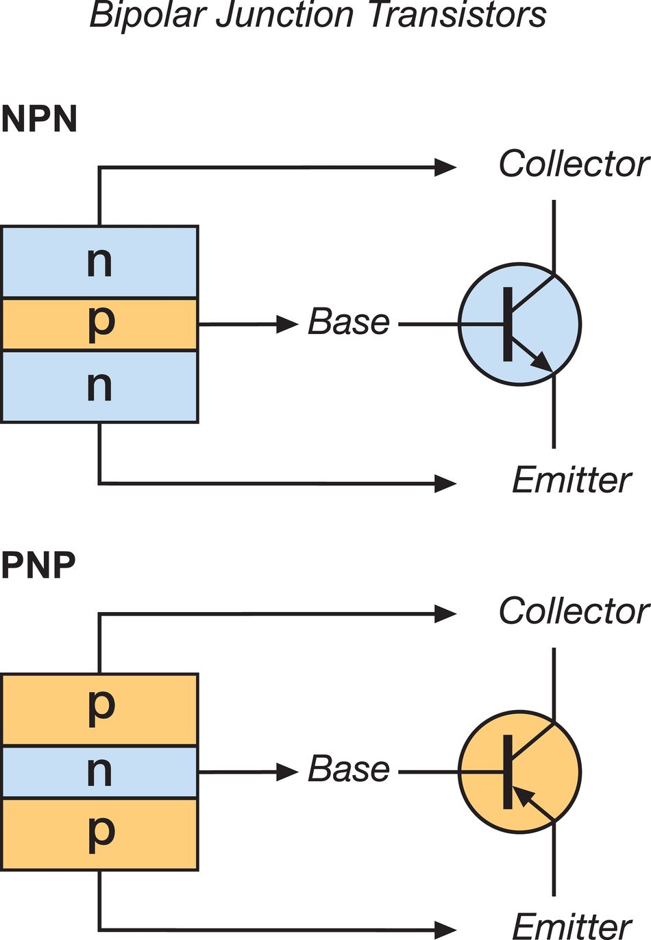
In a Bipolar Junction Transistor (BJT), the three terminals are emitter, base, and collector. BJTs form two PN junctions. When the base–emitter junction is forward‑biased and the base–collector junction is reverse‑biased, current carriers flow across the thin base region and are collected, allowing the transistor to conduct.
There are two types of BJTs:
NPN BJT: an N‑type emitter and collector separated by a thin P‑type base.
PNP BJT: a P‑type emitter and collector separated by an N‑type base.
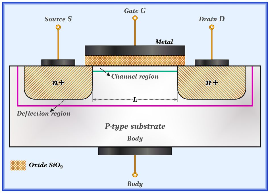
Field-Effect Transistor (FET)
In a Field‑Effect Transistor (FET), the terminals are the source, gate, and drain. The structure involves layers of doped semiconductor material. In FETs, the channel conductivity is controlled by the electric field. This field is controlled by the applied voltage, and therefore, they are called voltage-controlled transistors. There are two types of FETs:
N‑channel FET: an N‑type channel between source and drain with a P‑type substrate.
P‑channel FET: a P‑type channel in an N‑type substrate.
Current‑Controlled vs Voltage‑Controlled Devices
The key distinction between BJTs and FETs lies in their control mechanism.
BJTs are current‑controlled devices. It means that a small base current causes a larger current between emitter and collector.
FETs are voltage‑controlled: a voltage applied to the gate relative to the source alters the conductivity of the channel between source and drain.
The high input impedance of FETs arises because the gate terminal is insulated by an oxide layer (in MOSFETs). Sovirtually, no current flows into the gate. This makes FETs ideal for switching applications where control signals must not load preceding stages. BJTs have lower input impedance but typically higher gain and lower output impedance, which can be advantageous for certain amplifiers.
Suggested Reading: Difference Amplifier: Theory, Design, and Applications for Engineers
Understanding Bipolar Junction Transistors (BJTs)
Operating Regions
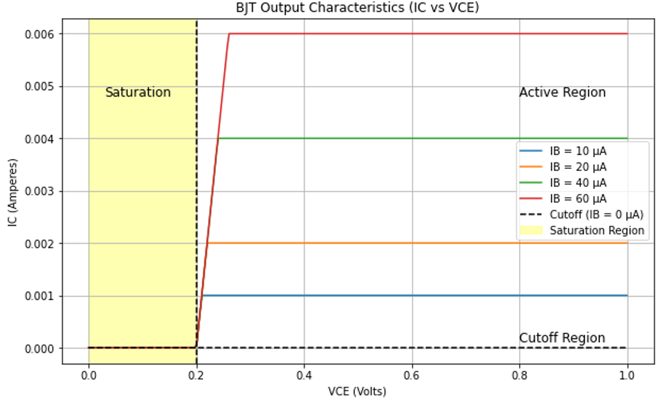
A BJT can operate in four regions determined by the base–emitter voltage (Vbe)and base–collector voltage Vbc junction biases:
Cut‑Off: Both junctions reverse-biased; no collector current flows. The transistor behaves as an open switch.
Active (Forward‑Active): In this region, base–emitter junction is forward- biased (~0.6 – 0.7 V for silicon), while the base–collector junction is reverse-biased. Collector current Ic is β times the base current Ib . This region is used for amplification.
Saturation: In this region, both junctions are forward biased. The transistor is fully on, with minimal collector–emitter voltage (V_CE(sat) ≈ 0.1 – 0.3 V). Used for switching.
Reverse‑Active: Base and collector are swapped relative to the bias. But this configuration is rarely used.
Amplifier Operation
In amplification applications, the BJT is biased in the active region. The collector current is given by:

where β (beta) is the current gain hFE, for general‑purpose transistors like the BC547 or 2N3904, β can be around 100. It means that a base current of 0.1 mA controls a collector current of approximately 10 mA. The relation is given as:

Biasing and Resistor Calculation
Since the base‑emitter junction behaves like a diode, it usually requires about 0.7 V to turn on an NPN BJT. So, for a 9 V supply, 8.3 V remains across the base resistor. So, given the base current, the base resistor value can be calculated using Ohm’s law. For instance, to achieve 0.1 mA base current, the calculation yields a resistance of approximately 83kΩ.
A standard value like 82 kΩ is close enough. The collector resistor Rc sets the collector current and voltage swing. With proper biasing, we can ensure linear operation and prevent saturation or cutoff in analog circuits.
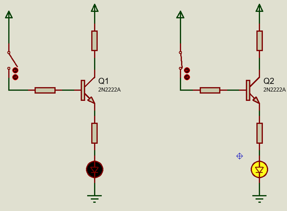
NPN Transistor as a Switch
A simple switch circuit uses an NPN transistor to drive an LED. When the base is pulled high through a resistor, the transistor saturates and the LED lights. When the base is low, the transistor is off, and the LED is dark.
Biasing and Resistor Calculation
Since the base‑emitter junction behaves like a diode, it usually requires about 0.7 V to turn on an NPN BJT. So, for a 9 V supply, 8.3 V remains across the base resistor. So, given the base current, the base resistor value can be calculated using Ohm’s law. For instance, to achieve 0.1 mA base current, the calculation yields a resistance of approximately 83kΩ.
A standard value like 82 kΩ is close enough. The collector resistor Rc sets the collector current and voltage swing. With proper biasing, we can ensure linear operation and prevent saturation or cutoff in analog circuits.
Example of an NPN Switch
A simple switch circuit uses an NPN transistor to drive an LED. When the base is pulled high through a resistor, the transistor saturates and the LED lights. When the base is low, the transistor is off, and the LED is dark.
Choosing a BJT for Switching Applications
The important parameters to consider when selecting a BJT are:
Maximum Collector current (Ic max)
Maximum Collector–emitter voltage (Vce max)
Gain (β) at operating current.
Power dissipation Pd.
For switching high currents or high voltages, consider using a MOSFET or IGBT instead of a small signal BJT.
Suggested Reading: Transistor as a Switch: Theory and Practical Implementation for Digital and Hardware Engineers
Understanding Field‑Effect Transistors (FETs)
Types of FETs
There are several types of FETs, each having specific applications in terms of power handling and switching speed. They are generally categorized by gate structure and operation mode. The following table summarizes the different FET types.
FET Type | Channel | Modes | Key Features |
JFET (Junction Field‑Effect Transistor) | N‑channel or P‑channel | Depletion mode only | Conducts at zero gate bias; gate voltage controls channel depletion. |
MOSFET (Metal‑Oxide‑Semiconductor FET) | N‑channel or P‑channel | Enhancement or depletion | Insulated gate; extremely high input impedance; widely used. |
IGFET (Insulated‑Gate FET) | General term for MOSFET | Enhancement/depletion | Another name for MOSFET. |
IGBT (Insulated‑Gate Bipolar Transistor) | Combines MOS gate with BJT output | Enhancement | Used for high‑power switching; not covered in detail here. |
Enhancement‑mode MOSFETs are normally off. They conduct when a gate‑source voltage Vgs exceeding the threshold Vth induces a channel.
Depletion‑mode MOSFETs are normally on. A bias of the opposite polarity can pinch off the channel.
Suggested Reading: Enhancement vs Depletion MOSFETs: Design, Applications & Future Trends
Operating Regions
When used as switches, FETs operate in two primary regions:
Cut‑Off (OFF): In this region, Vgs < Vth.The channel is not formed; no drain current flows, and the device appears as an open switch. In an N‑channel MOSFET, grounding the gate turns it off.
Saturation (ON): In the saturation region, Vgs >> Vth. Hence, a conductive channel forms. The drain current reaches its maximum, limited by circuit resistance. The MOSFET behaves like a low‑resistance closed switch.
Example: MOSFET Switch
Consider an N‑channel enhancement MOSFET like the BS170. Its gate threshold voltage is about 2.1 V To turn it on fully, V_GS must exceed this threshold by a margin (e.g., 4 – 5 V).
When used with a microcontroller, ensure the logic high output can provide adequate gate voltage; otherwise, use a gate driver or a logic‑level MOSFET. Because the gate draws negligible current once charged, MOSFETs are ideal for low‑power switching.
Recommended Reading: How Do MOSFETs Work: Comprehensive Technical Guide for Engineers (2025)
Transistor as a Switch vs Amplifier
Transistors are versatile because they can act either as analog amplifiers or digital switches. The intended region of operation determines circuit topology and biasing.
Switching Applications
In digital electronics, transistors toggle between on and off states, representing binary 1s and 0s. When a small voltage/current is applied to the base (BJT) or gate (FET), it controls a larger current between collector–emitter or drain–source.
Key considerations include:
Operating Region: Use cut‑off (OFF) and saturation (ON) for BJTs; cut‑off and saturation (also called triode) for MOSFETs.
Saturation Overdrive: Overdriving the base/gate ensures the transistor fully turns on. For BJTs, the base current is chosen so that Ib ≥ Ic/β.
Switching Speed: BJTs suffer from minority‑carrier storage delay; MOSFETs switch faster but have gate capacitance. High‑speed applications may require specialized drivers and minimize transition times to reduce power loss.
Flyback Protection: Inductive loads (relays, motors) need a flyback diode across the load for BJTs. MOSFETs often include body diodes but may still require external diodes for high currents.
Amplification Applications
In amplifiers, transistors operate in the active region. Common amplifier topologies include:
Common Emitter (CE) / Common Source (CS): Provides voltage gain; phase inversion occurs.
Common Collector (Emitter Follower) / Common Drain (Source Follower): Provides current gain with voltage buffering; output follows input (unity gain).
Common Base / Common Gate: Less common; used at high frequencies due to low input impedance.
Biasing networks (voltage dividers, emitter/source resistors) establish the quiescent operating point (Q‑point) to maximize signal swing without distortion.
Practical Design Considerations
Selecting Component Values
When designing a transistor switch or amplifier, follow these steps:
Determine the load current and voltage requirements.
Choose between a BJT or MOSFET, keeping in mind the current ratings and power dissipation values.
Calculate the Base/Gate drive current. For BJTs, it is best to provide at least twice the calculated base current. For MOSFETs, make sure that the gate voltage exceeds by a sufficient margin. Typically a gate resistor of 10 to 100 Ohms is used to damp the oscillations.
Add heat sinks to the transistors, especially when using for high-speed siwtching or high-power applications.
Use protective components like flyback diodes, zener diodes, and snubber networks to protect the circuitry.
Example Circuit: Driving a Relay with an NPN BJT
Load: A relay coil draws 50 mA at 5 V.
Transistor Selection: Choose a general‑purpose NPN transistor with Ic(max) ≥ 100 mA (e.g., 2N2222).
Base Current: For β = 100, IB=50 mA/100=0.5 mA. Use 1 mA to ensure saturation.
Base Resistor: If you’re driving the relay from a 5 V microcontroller:
Rb(5 V−0.7 V)/1 mA≈4.3 kΩ In this case, choose the standard value of 4.7 kΩ.- Flyback Diode: Place a 1N4148 or 1N4001 diode across the relay coil (cathode to supply, anode to transistor collector).
Transistors in Digital Logic and Hardware Applications
Logic Gates and CMOS
Digital logic relies on transistors arranged as logic gates. Complementary MOS (CMOS) technology uses pairs of N‑channel and P‑channel MOSFETs to implement logic functions with near‑zero static power consumption.
In a CMOS inverter, a PMOS transistor connects the output to Vdd when the input is low, while an NMOS transistor connects the output to ground when the input is high. Complex logic gates (NAND, NOR, XOR) are built by arranging multiple MOSFETs in series or parallel.
Suggested Reading: NMOS and PMOS Transistors: Fundamentals and Applications
Integrated Circuits and Processor Transistor Counts
Integrated circuits (ICs) contain millions to billions of transistors. According to recent records, the highest transistor count in a consumer microprocessor as of 2025 is 184 billion transistors in Apple’s M3 Ultra system‑on‑chip, fabricated using a 3 nm process.
GPUs like Nvidia’s B100 (208 billion transistors) push transistor counts even higher, while specialized AI chips can integrate trillions of MOSFETs using 3D stacking.
Transistor density improvements have historically followed Moore’s law, which predicted a doubling of transistors roughly every two years.
While physical scaling is reaching atomic limits, innovations such as chiplet architectures, 3D integration, and new materials (SiC, GaN, MoS₂) continue to enhance performance.
Suggested Reading: Where GaN can, it should, and GaN can in more and more places
Analog and Mixed‑Signal Circuits
Transistors are fundamental to analog blocks such as amplifiers, voltage regulators, oscillators, and filters. Operational amplifiers contain differential pairs of BJTs or MOSFETs. Mixed‑signal ICs integrate analog front ends with digital logic, using transistors to perform analog‑to‑digital conversion and filtering.
Suggested Reading: Difference between Active and Passive Filters?
Power Electronics
Power transistors control large currents and voltages in motor drives, power supplies, and renewable‑energy converters. Insulated‑gate bipolar transistors (IGBTs) combine MOSFET gate input with BJT output characteristics for high‑voltage switching.
Wide‑bandgap devices (SiC, GaN) offer lower losses and higher switching frequencies, enabling efficient electric vehicle chargers and solar inverters.
Suggested Reading: Are GaN semiconductor power components ready for automotive?
Market Trends and the Future of Transistors
Global Market Statistics
The transistor market reflects the pervasiveness of these devices in electronics. Mordor Intelligence reports that the global transistor market size reached US$ 18.63 billion in 2025. It is projected to grow to US$ 26.82 billion by 2030, representing a compound annual growth rate (CAGR) of 7.56%. Key insights include:
Bipolar‑junction transistors (BJTs) accounted for 48.8% of revenue in 2024.
Silicon devices retained 69.3% share in 2024, but wide‑bandgap materials like SiC and GaN are the fastest‑growing segment.
Asia‑Pacific led the market with a 56.3% revenue share in 2024, driven by China’s localization and India’s manufacturing incentives.
Growth drivers include power‑efficient mobile SoCs, electric vehicle electrification, AI/ML edge inference, 5G‑to‑6G RF upgrades and government incentives for wide‑bandgap fabs.
Conclusion
Transistors are the building blocks of modern electronics. Understanding the working of a transistor from scratch, i.e., from semiconductor physics and device structures to operating regions and practical circuit design, is critical for engineers. It allows them to design reliable systems. Fundamentally, BJTs and FETs are different. BJTs are current‑controlled and suited to high‑gain amplification, while FETs are voltage‑controlled and excel in switching with high input impedance. When it comes to practical designs, it requires careful biasing, resistor calculations, and appropriate device selection.
In digital logic, billions of transistors implement logic functions and memory, while power electronics rely on robust transistors for efficient energy conversion. The market trends show strong growth driven by mobile devices, electric vehicles, and 5G infrastructure. In the future, wide‑bandgap semiconductors, 3D integration, and novel device structures will be more prevalent. Therefore, engineers and students should continue to explore transistor behavior through hands‑on experiments and design projects.
Frequently Asked Questions
1. What is the difference between a BJT and a MOSFET?
A BJT is a current‑controlled device where base current regulates collector current, making it suitable for current amplification. A MOSFET is a voltage‑controlled device where gate voltage controls drain current. MOSFETs offer very high input impedance and faster switching, but may require gate driver circuits. BJTs generally have higher gain and can handle higher current density, but suffer from slower switching due to charge storage.
2. Why is 0.7 V needed to turn on an NPN transistor?
The base–emitter junction of a silicon BJT behaves like a diode with a forward voltage of approximately 0.6 – 0.7 V. When this voltage is applied, carriers are injected across the junction, allowing the transistor to conduct. Without sufficient forward bias, the junction remains reverse-biased, and the transistor stays off
3. How do I choose the right resistor for a transistor base or gate?
Determine the desired base or gate current/voltage. For a BJT, calculate base current, then compute Rb. For MOSFETs, ensure the gate voltage exceeds the threshold by a safe margin; a small gate resistor (tens of ohms) limits inrush current and dampens oscillations.
4. Can one transistor switch high-power loads?
A single small transistor can switch modest loads (tens to hundreds of milliamps). For high-power loads (amps or more), use a power MOSFET or IGBT with adequate current rating and heat dissipation. Consider using a driver stage or a Darlington pair for BJTs. Always include proper heat sinking and protective circuits.
5. What causes transistor saturation, and why can it slow switching?
Saturation occurs when both the base–emitter and base–collector junctions are forward-biased, resulting in maximum collector current and minimal collector–emitter voltage. During saturation, excess charge accumulates in the base region. To turn off the transistor, this stored charge must be removed, which slows the transition. Over‑driving the base may ensure saturation, but increases charge storage and delay.
6. How has transistor technology evolved?
Transistor counts have increased dramatically. Early CPUs like Intel’s 4004 (1971) contained 2,300 transistors; modern processors like Apple’s M3 Ultra integrate 184 billion transistors. Device scaling has followed Moore’s law, though physical limits are approaching. Innovations such as chiplets, 3D stacking, wide‑bandgap materials, and novel FET structures are enabling continued performance gains.
7. What are wide‑bandgap transistors, and why are they important?
Wide‑bandgap semiconductors (SiC, GaN) have larger energy gaps than silicon. This allows devices to operate at higher voltages, temperatures, and switching frequencies with lower losses. SiC MOSFETs and GaN HEMTs are increasingly used in electric vehicles, renewable‑energy converters, and RF amplifiers. The transistor market is seeing rapid growth in these segments.
References
Electronics‑Tutorials. Transistor Tutorial Summary—overview of BJT and FET operation, biasing and differences. Available at: electronics-tutorials.ws
Øyvind Nydal Dahl, How Transistors Work – A Simple Explanation—practical BJT and MOSFET examples and resistor calculations. Available at: build-electronic-circuits.com
Mordor Intelligence, Transistor Market Size & Share Analysis—market statistics and trends for 2025–2030. Available at: mordorintelligence.com
Wikipedia (transistor count) — records of transistor counts in modern processors. Available at: en.wikipedia.org
in this article
1. Key Takeaways2. Introduction3. Fundamentals of Transistors4. Understanding Bipolar Junction Transistors (BJTs)5. Understanding Field‑Effect Transistors (FETs)6. Transistor as a Switch vs Amplifier7. Practical Design Considerations8. Transistors in Digital Logic and Hardware Applications9. Market Trends and the Future of Transistors10. Conclusion11. Frequently Asked Questions12. References