Transistor as a Switch: Theory and Practical Implementation for Digital and Hardware Engineers
This technical article explains how a transistor as a switch operates. It covers theoretical foundations, bipolar and MOSFET operating regions, practical design calculations, and real world applications.

21 Aug, 2025. 16 minutes read
Transistor as a Switch
Introduction
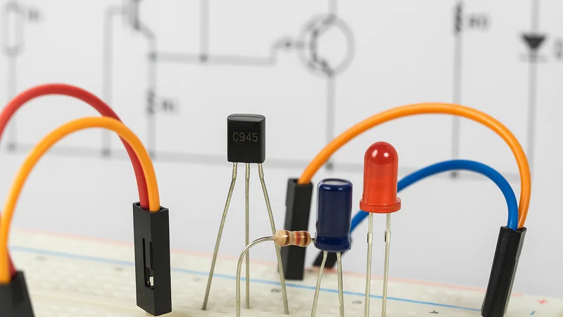
In modern electronics, the transistor as a switch is one of the most fundamental and widely used applications, forming the backbone of both digital logic circuits and hardware control systems. By operating a transistor in its cutoff and saturation regions, engineers can achieve reliable on/off control for a variety of loads, from LEDs to high-power devices. The transistor as a switch refers to using a transistor not as a linear amplifier but as a binary device that is either fully on (conducting) or fully off (blocking).
For digital and hardware engineers, understanding the electrical characteristics, biasing requirements, and switching speed is essential for optimal circuit performance. Whether in low-voltage embedded designs or high-frequency power electronics, the transistor as a switch ensures precise control with minimal energy loss. This article explores the theory, design considerations, and real-world implementation of the transistor as a switch, providing practical insights for engineers seeking robust and efficient switching solutions.
Why Switching Matters?
Digital electronics operate on binary logic, where signals are represented as either logical “1” or logical “0”. When implementing the transistor as a switch, the cutoff region corresponds to a non-conductive state, effectively outputting a logic high when pulled up to the supply voltage, while the saturation region represents a fully conductive state, producing a logic low when the output is near ground potential.
In power electronics, switching operation is equally critical. By ensuring the transistor transitions rapidly between cutoff and saturation, it spends minimal time in the active (linear) region — the point where both voltage and current are significant, resulting in unwanted I × V power dissipation. [1] Reducing this transition time minimizes heat generation, increases efficiency, and prolongs component life.
High-speed switching is the foundation of DC–DC converters, pulse-width modulation (PWM) motor controllers, and digital signal processing hardware. The ability to operate at higher frequencies allows for smaller passive components, faster response times, and improved energy efficiency. Proper biasing, gate/base drive circuitry, and load matching are therefore essential to fully exploit the advantages of the transistor as a switch in both low-power logic systems and high-performance power applications.
Recommended Reading: Types of Switches: Complete Engineering Guide for 2025
Fundamental Switching Theory
Operating Regions of Bipolar Junction Transistors (BJTs)
A bipolar junction transistor (BJT) is a three-terminal, current-controlled device consisting of the emitter (E), base (B), and collector (C). It can operate in four modes: cut-off, saturation, active, and reverse-active. For transistors as switch applications, only the cut-off (OFF) and saturation (ON) regions are desirable. The operating mode is determined by the polarity and magnitude of the base emitter voltage (VBE) and base–collector (VBC) voltage.
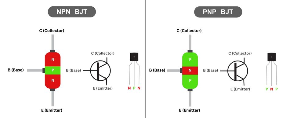
Cut-Off Region (OFF) – In the cut-off region, the base-emitter junction is reverse-biased. The base and emitter are grounded, and VBE < 0.7 V for silicon devices. Both junctions are reverse-biased, no collector current flows, and the transistor behaves like an open switch. The collector voltage equals the supply voltage (VCC), representing a logic high.
Saturation Region (ON) – In the saturation region, the base–emitter and base–collector junctions are forward-biased. The base input is driven high so that VBE > 0.7 V and sufficient base current flows. This results in maximum collector current and minimum collector–emitter voltage drop. The transistor conducts like a closed switch, and the output approaches ground (logic low). The practical devices exhibit a small saturation voltage.
The simple rule of thumb for BJT switching is to overdrive the base so the transistor saturates. However, the base current increases power dissipation and slows turn-off, since stored charge in the emitter junction must be removed before the device re-enters the cut-off region.
Operating Regions of Metal‑Oxide Semiconductor FETs (MOSFETs)
MOSFETs are three‑terminal, voltage‑controlled devices with gate (G), source (S) and drain (D). Enhancement‑mode N‑channel MOSFETs are commonly used as switches. [2] Because the gate is insulated, the input resistance is extremely high, so virtually no gate current flows. MOSFETs also operate in cut‑off and saturation regions when used as switches.
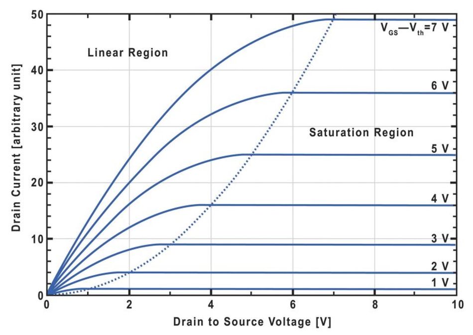
Cut-Off Region (OFF) – When the gate‑source voltage is below the threshold voltage, no conduction channel forms. With the gate grounded, the MOSFET is off; there is no drain current and the drain–source voltage equals the supply. The device acts as an open switch.
Saturation Region (ON) – When gate‑source voltage is much greater than the threshold voltage, a conductive channel forms. The drain current reaches its maximum and the channel on‑resistance becomes small. Ideally the drain–source voltage equals zero; in practice the on‑resistance leads to a small voltage drop. The MOSFET thus behaves like a low‑resistance closed switch.
Unlike BJTs, MOSFETs are majority carrier devices, so they do not suffer from minority carrier storage delay, enabling much higher switching speeds. However, the gate terminal exhibits parasitic capacitances that must be charged and discharged quickly to achieve high-speed operation, often requiring dedicated gate driver circuits.
Comparison of BJTs and MOSFETs
The table below summarises the key differences relevant to switching. A BJT is current‑controlled, while a MOSFET is voltage‑controlled. MOSFETs have higher input impedance and can switch faster; BJTs often have higher current gain but suffer from storage delay. Engineers must weigh these factors when choosing a device for switching applications:
| Feature | Bipolar Junction Transistor | MOSFET | Implication |
| Control Type | Base current controls collector current | Gate voltage controls drain current | MOSFETs require negligible gate current; BJTs require continuous base drive |
| Input Impedance | Moderate (kΩ range), lower noise immunity | Very high input impedance (voltage‑controlled) | MOSFETs are easier to interface with logic outputs |
| Switching Speed | Slower due to storage time; switching speed is slower than MOSFET | High switching speed and minimal storage delay | MOSFETs excel in high‑frequency switching applications |
| Power Efficiency | Higher saturation losses and heat | Lower on‑resistance and reduced heat | MOSFETs provide better efficiency for low‑loss switching |
| On-State Voltage Drop | Common Emitter Voltage (sat) ≈ 0.05–0.2 V | Dependent on RDS(on); typically tens of milliohms | MOSFETs can achieve lower conduction losses |
| Cost and Complexity | Typically cheaper; simple drive circuits | Generally more expensive; sensitive to electrostatic discharge | BJT switches are often used for low‑cost, low‑frequency designs |
By mastering cut-off and saturation principles, you lay the groundwork for reliable digital control and energy-efficient hardware performance.
Recommended Reading: Linear vs Switching Power Supply: Understanding the Differences
BJT Switching in Detail
Biasing for Saturation and Cut‑Off
To use a BJT as a switch, the base bias must move the device between cut‑off and saturation. In an NPN transistor the emitter is connected to ground and the collector to the load and supply. A base resistor limits the base current. When the input voltage is low (below ~0.7 V), the transistor is cut‑off (open switch). When the input signal is high and base current flows, the device saturates and acts like a closed switch.
Calculating Base Resistor
To ensure saturation, base current must exceed the minimum needed for the desired collector current, accounting for the current gain (β) of the transistor:

Where β forced is chosen lower than the typical β to guarantee saturation (often β forced ≈ β/2 to β/5).
Example:
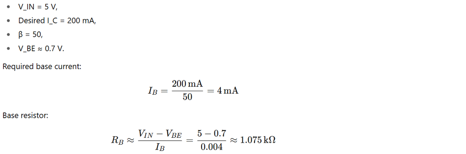
So, choosing the nearest lower standard value (e.g., 1 kΩ) ensures reliable saturation.
Switching Dynamics: Turn-On and Turn-Off Times
Switching speed is influenced by parasitic capacitances and carrier storage effects.
Turn-On Time:

Where,
td (delay time) = time for collector current to rise from 0 to 10 % of Ic (sat)
tr (rise time) = time to rise from 10 % to 90 % of Ic (sat)
Turn-Off Time:

Where:
ts (storage time) = time carriers remain in the base after input is removed
tf (fall time) = time for Ic to fall from 90 % to 10 % of Ic (sat)
The carrier storage in deep saturation increases ts, making the transistor slower to turn off. Engineers reduce storage time by avoiding deep saturation (e.g. using Schottky clamped BJTs) or using MOSFETs. Speed‑up capacitors across the base resistor and negative drive signals at turn‑off can also hasten discharge of the base.
Practical Considerations
Leakage Current in Cut-Off
Even in cut-off, small leakage currents flow due to minority carrier injection:

For most low-voltage digital circuits, this current (μA range) is negligible.
Saturation Voltage Impact
The collector current in saturation is:

The knee voltage is small (tens of millivolts) so the transistor remains efficient in switching mode.
Flyback Diode for Inductive Loads
When switching inductive loads, a flyback diode in reverse bias across the load prevents high-voltage transients from exceeding the transistor’s breakdown voltage. The diode provides a discharge path for stored magnetic energy:

High-Side Switching
For loads connected to ground, an NPN transistor is used as a low-side switch. For high-side switching, a PNP transistor or P-channel MOSFET is preferred. In a PNP transistor, the emitter voltage must be higher than the base voltage by ~0.7 V to conduct.
Mastering BJT switching requires precise biasing, timing control, and protection techniques. With correct design, BJTs deliver reliable, efficient performance in digital and power applications, making them a versatile choice for engineers across industries.
Recommended Reading: Understanding NPN vs PNP Transistors: A Comprehensive Guide
MOSFET Switching in Detail
Biasing for Enhancement-Mode MOSFETs
The enhancement-mode N-channel MOSFET is naturally off when VGS = 0. It turns on when VGS exceeds the threshold voltage (VTH), typically 2–4 V for logic-level devices, and higher for standard-level types.
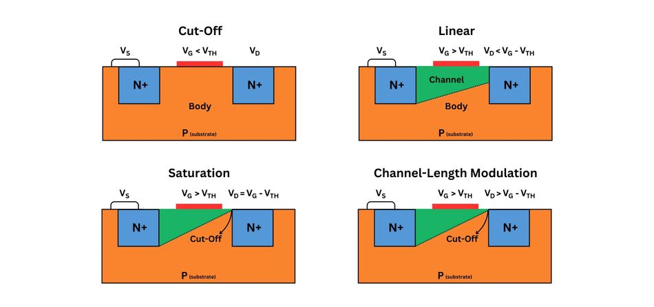
Cut-Off (OFF) – Gate and source are at the same potential , no conduction channel forms, and drain current (ID) is effectively zero. The output voltage at the drain equals VDD.
On-State (Saturation/Linear) – Raising VGS to the supply voltage (VDD) enhances the channel, drastically reducing on-resistance (RDS(on)). For power MOSFETs, RDS(on) can be just a few milliohms; for small-signal MOSFETs, it may be several ohms. A low RDS(on) minimizes voltage drop and conduction losses:

The device selection focuses on ensuring RDS(on) is low enough for the required load current while keeping dissipation within safe limits.
Gate Drive and Resistor Considerations
Despite no continuous gate current flows, the gate capacitances must be charged and discharged for switching.
The gate resistor limits inrush current and damps oscillations caused by parasitic inductances.
Larger gate resistor values slow transitions, reducing EMI but increasing switching losses.
For high-frequency or large-gate MOSFETs, dedicated gate driver ICs deliver several amps of peak current to rapidly overcome gate charge.
The approximate gate charging time can be estimated as:

Inductive Load Protection
Like BJTs, MOSFETs require flyback diodes or snubber networks when switching inductive loads (motors, relays, solenoids).
The flyback diode placed across the load, reverse-biased in normal operation, safely dissipates stored energy when the MOSFET turns off.
For high-speed switching, a Schottky diode is often preferred due to its low forward voltage and fast recovery.
High-Side Switching Strategies
P-Channel MOSFETs: Naturally suited for high-side switching; they turn on when VGS < 0 (gate pulled below source). They are simpler to drive but have higher RDS(on) and thus greater conduction losses.
N-Channel MOSFETs: Preferred for efficiency; require a bootstrap or charge-pump driver to generate a gate voltage higher than the source (VGS > VTH) when the source is near VDD.
MOSFET Characteristics and Switching Behavior
Cut-Off Characteristics:
VGS < VTH, no channel formed, ID ≈ 0, VDS ≈ VDD.
On-State Characteristics:
VGS ≫ VTH, RDS(on) minimal, VDS ≈ 0, maximum load current flows.
Switching Table Summary:
| Device Type | OFF Condition | ON Condition | Typical Use |
| N-Channel Enhancement | VGS < VTH | VGS > VTH | Low Side Switching |
| P-Channel Enhancement | VGS > -VTH | VGS < -VTH | High Side Switching |
Switching Speed Advantages
MOSFETs are majority carrier devices, eliminating the minority carrier storage delay seen in BJTs. [3] This results in:
Faster turn-off (no charge tail)
Shorter total switching time
Higher efficiency at high frequencies (DC-DC converters, SMPS)
The switching loss can be approximated as:

Choosing Between N-Channel and P-Channel MOSFETs
N-Channel: Lower cost, lower RDS(on), better efficiency. Ideal for low-side switching and high-side designs with bootstrap drivers.
P-Channel: Easier high-side implementation without special drivers, but higher RDS(on) and conduction losses make them less efficient for high-current loads.
MOSFET switching mastery demands careful device selection, precise gate drive design, and effective protection for varying loads. With optimized biasing and layout, MOSFETs deliver unmatched speed and efficiency in modern high-frequency power and digital applications.
Recommended Reading: How Do MOSFETs Work: Comprehensive Technical Guide for Engineers (2025)
Practical Design Guidelines
Step‑By‑Step BJT Switching Design
Determine Load Current and Supply Voltage: For example, if a microcontroller pin must drive a 12 V relay coil drawing 50 mA, the transistor must handle at least 50 mA and withstand VCE equal to the supply voltage.
Select a Transistor with adequate Current Rating and β: Choose a general‑purpose NPN (e.g. 2N2222 or BC337) for currents up to a few hundred milliamps. For higher currents use a Darlington transistor or a power BJT.
Compute Base Resistor. Use RB ≈ (VIN – VBE) / (Ic/β): Include a margin by driving the base with twice the minimum required current to guarantee saturation. For microcontrollers with limited output current (e.g. 20 mA per pin) use an intermediate driver transistor or MOSFET.
Add a Flyback Diode across Inductive Loads: Connect the diode in reverse across the load so that when the transistor turns off, the induced voltage circulates current through the diode instead of the transistor.
Verify Power Dissipation: Ensure that P = Ic² × RCE(sat) remains within the transistor’s power rating. Use a heatsink if necessary.
Step‑By‑Step MOSFET Switching Design
Determine Gate Drive Voltage: Verify that the available logic level is sufficient to fully enhance the MOSFET. For 5 V logic, choose a MOSFET with VTH ≤ 2–3 V and RDS(on) specified at VGS = 4.5 V.
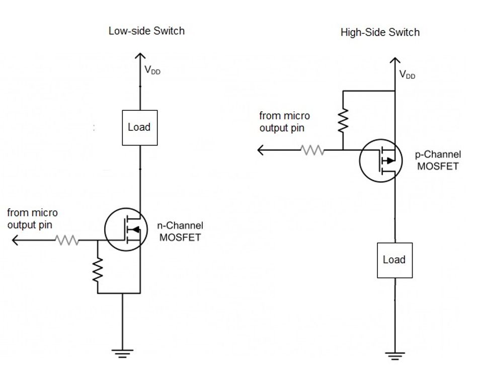
Select appropriate N‑channel or P‑channel Device: For low‑side switching choose an N‑channel MOSFET; for high‑side choose a P‑channel or use a high‑side driver for an N‑channel MOSFET.
Calculate the Gate Resistor: Start with values between 50 Ω and 200 Ω to limit current spikes and ringing. Adjust based on the desired rise/fall times and driver capability. If switching large MOSFETs, consider using a gate driver IC.
Add a Flyback Diode or Snubber across Inductive Loads: For high‑frequency switching, add a snubber RC network or a transient voltage suppressor to reduce voltage spikes.
Ensure Thermal Limits: Calculate conduction loss (ID² × RDS(on)) and switching loss (½ × CGD × VDD² × fsw). Ensure that the total power dissipation stays within the thermal rating of a MOSFET. Use proper PCB copper area or heatsinking for power devices.
High‑Side vs Low‑Side Switching
Low‑side switching uses an NPN BJT or N‑channel MOSFET with the load connected to the supply and the transistor to ground. This configuration is simple and cost‑effective, but leaves the load connected to VCC when off. High‑side switching places the transistor between the supply and the load so that the load is truly isolated when off. PNP BJTs or P‑channel MOSFETs are used for high‑side switching; the base or gate is driven lower than the emitter or source to turn on. High‑side N‑channel MOSFETs require gate voltages above the supply, achieved using charge pumps or bootstrap circuits.
Darlington and Compound Transistor Switches
If a single BJT’s current gain is insufficient, two BJTs can be cascaded in a Darlington pair. The first transistor’s emitter drives the base of the second, resulting in an overall current gain equal to the product of individual gains. Darlington transistors allow small base currents to switch large collector currents but at the cost of higher V_CE(sat) and slower switching due to increased storage charge.
Similarly, transistor arrays (e.g. ULN2803A) integrate multiple Darlington NPN transistors with built‑in flyback diodes, simplifying the design of relay and stepper motor drivers.
The effective practical design starts with aligning device parameters, biasing networks, and protection components to the application’s demands. By integrating sound layout practices with precise calculations, engineers can ensure reliable, efficient, and durable switching performance in real-world circuits.
Testing and Optimization of Switching Circuits
The switching theory and design are only effective when validated in real-world conditions. Careful testing, measurement, and optimization ensure that BJTs and MOSFETs meet speed, efficiency, and reliability targets under actual operating loads and environments.
Measuring Switching Waveforms
An oscilloscope is the primary tool for analyzing transistor switching behavior. By observing VCE/ VDS and Ic / Id waveforms simultaneously with a current probe or shunt resistor, engineers can visualize the exact transitions during turn-on and turn-off.
Look for signs of overshoot, ringing, or slow edges, which indicate excessive parasitic inductance, insufficient drive strength, or PCB layout issues. Capturing these waveforms at different loads and supply voltages reveals performance boundaries and highlights where optimizations are needed.
Verifying Timing Parameters
Measure delay time, rise time, storage time, and fall time to verify switching speed. You can compare these to datasheet values at the intended VCC / VDD, load, and temperature. If you’re new to all of this, you may consult tutorials online.
The significant deviations often point to underdriven gates/bases, incorrect bias resistor values, or thermal effects. For MOSFETs, excessive rise/fall times can be corrected by reducing gate resistance or increasing driver current capability. For BJTs, avoiding deep saturation and using Baker clamps can reduce storage time.
Thermal Characterization
Even with correct biasing, thermal performance determines long-term reliability. Use infrared cameras, thermocouples, or integrated thermal sensors to monitor junction temperature under worst-case load and ambient conditions.
If the junction temperature approaches the maximum of the manufacturer, improve heat dissipation by increasing copper pour area, adding heatsinks, or reducing switching/conduction losses through device selection or gate/base drive tuning. Thermal runaway in BJTs and excessive RDS(on) rise in MOSFETs can be prevented through proactive thermal management.
Efficiency Optimization
Total losses are the sum of conduction loss and switching loss:

Optimize gate/base drive, reduce unnecessary capacitance, and fine-tune component placement to minimize these losses. Layout improvements, such as minimizing drain/collector trace length and using low-inductance paths, can further reduce parasitics and improve switching efficiency.
Reliability and Stress Testing
Accelerated life tests — operating the circuit at elevated temperatures, voltages, or currents reveal weaknesses in design margins. For inductive loads, confirm that flyback diodes, snubbers, or TVS suppressors effectively clamp voltage spikes under all switching conditions.
High-duty-cycle and thermal cycling tests ensure that solder joints, PCB traces, and connectors can withstand repeated stress without failure. Reliability testing is critical in automotive, aerospace, and industrial control applications where downtime is costly.
Testing and optimization bridgethe gap between theoretical design and dependable performance. By validating timing, thermal behavior, and efficiency under real conditions, engineers can fine-tune switching circuits for maximum reliability, longevity, and operational excellence.
Recommended Reading: Vcc vs Vdd: Differences, Usage, and Best Practices in Modern Electronics
Applications and Examples
Digital Logic Interfaces
Logic gates and microcontrollers often can source or sink only a few milliamps. Transistors provide the interface to drive larger loads while preserving logic levels. In transistor‑transistor logic (TTL), BJTs operate in saturation and cut‑off to represent logic “0” and “1”. Each NAND or NOR gate uses multiple transistors configured to saturate and cut off quickly. Modern CMOS logic uses complementary MOSFET pairs, where an N‑channel device pulls the output low and a P‑channel device pulls the output high. Because MOSFETs switch faster and consume less static power, CMOS has supplanted TTL in most digital applications.
Driving LEDs and Lamps
For small loads such as LEDs, a BJT or MOSFET switch allows a microcontroller to control the light without overstressing the pin. For example, a 20 mA LED connected to 12 V can be driven via an NPN transistor with a 560 Ω collector resistor and a base resistor sized to provide ~2 mA base current. In MOSFET applications, logic‑level N‑channel MOSFETs (e.g., BS170) can switch LED strings with negligible voltage drop. [4]
Controlling Relays and Solenoids
Relays and solenoids have inductive coils requiring tens to hundreds of milliamps at voltages up to 24 V. A transistor as a switch is used to sink the coil current; a flyback diode protects the transistor from voltage spikes. Because relays switch slowly, BJT storage time is less critical. For higher power loads or PWM control, MOSFETs are preferred.
Motor Drivers and PWM Control
DC motors draw significant current and exhibit inductance. MOSFETs are typically employed due to their low on‑resistance and fast switching. In H‑bridge configurations, four MOSFETs provide bidirectional control. Gate drivers ensure rapid transitions to minimise switching losses and electromagnetic interference.
Power Conversion and Switching Regulators
Switch‑mode power supplies (SMPS) rely on fast transistors switching tens or hundreds of kilohertz. MOSFETs dominate because their switching losses are lower, and they can handle high currents with low conduction loss. For example, a 24 W lamp controlled by a MOSFET with RDS(on) = 0.1 Ω dissipates only 0.4 W (I²R) plus switching losses. BJTs are rarely used in modern SMPS due to their slower switching and higher losses.
From simple LED drivers to complex motor controllers, switching devices enable precise, efficient control across countless systems. By studying real-world examples, engineers can translate theory into practical, high-performance designs tailored to diverse applications.
Recommended Reading: Extending the Battery Life of Hearables and Wearables with Single-Inductor Multiple-Output Switching Architecture
Advanced Techniques and Considerations
Speed‑Up Methods for BJTs
To mitigate the storage time penalty, designers use several techniques:
Baker Clamp (Schottky Diode): A diode between base and collector prevents the base–collector junction from saturating deeply, thereby reducing stored charge.
Speed‑Up Capacitors: A small capacitor in parallel with the base resistor provides an initial surge of base current to overcome capacitances quickly during turn‑on, and discharges during turn‑off via resistors to remove charge faster.
Active Pull‑Down: Using a complementary transistor or MOSFET to actively pull the base low during turn‑off reduces tail current and speeds up switching.
Dealing with Parasitic Capacitances in MOSFETs
Although MOSFETs lack minority carrier storage, the gate–source and gate–drain capacitances can slow switching if not driven properly. Gate driver ICs deliver large currents (ampere level) to charge/discharge the gate quickly. Snubber networks (RC or RCD) across the MOSFET reduce voltage overshoot and ringing when switching inductive loads.
High‑Side and Half‑Bridge Drivers
In half‑bridge or full‑bridge topologies, N‑channel MOSFETs provide efficient high‑side switching when used with gate drivers that generate gate voltages above the supply. Bootstrap circuits charge a capacitor during the low‑side on period and use it to drive the high‑side gate. Isolated gate drivers or charge‑pump controllers are necessary in isolated supplies and when the duty cycle approaches 100%.
These advanced techniques in switching design focus on pushing performance limits while maintaining reliability and efficiency. They include methods like active gate control, adaptive dead-time insertion, and snubber optimization to minimize switching losses and EMI.
Engineers also consider thermal management, PCB layout for reduced parasitic inductance, and advanced protection schemes such as overcurrent sensing and transient voltage suppression. By integrating simulation tools with real-world testing, these considerations ensure that designs meet constant speed, efficiency, and durability requirements in demanding applications.
Recommended Reading: Power Management for Tomorrow’s Innovations
Conclusion
Using a transistor as a switch transforms a continuous control element into a digital actuator. By driving a BJT between cutoff and saturation, or a MOSFET between cutoff and conduction, engineers implement logic functions, interface microcontrollers to loads, and build efficient power converters. Understanding the operating regions, biasing calculations, switching times, and device characteristics allows designers to choose the appropriate transistor type for a given application. BJTs are cost-effective and suitable for moderate currents, but they suffer from storage delay. MOSFETs offer faster switching, lower conduction losses and high input impedance, making them the default choice for modern digital and power electronics. Careful gate/base drive design, protective devices and thermal management ensure reliable and efficient switching in real‑world systems.
Frequently Asked Questions (FAQ)
1. Why use a transistor as a switch instead of a mechanical relay?
A. Semiconductor switches provide silent operation, faster switching times, smaller size and lower power consumption. Relays are still useful for isolating high voltages and currents, but switch much slower and wear out mechanically. They also lack the precise saturation region control seen in how transistors work.
2. How do I choose between a BJT and a MOSFET for switching?
A. Consider load current, required switching speed, and available gate/base drive. BJTs offer cost-effective amplification and provide good current gain, but have slower turn-off due to their storage time. MOSFETs are voltage controlled, switch faster and have lower on‑resistance but can be more expensive and require careful handling to avoid static damage.
3. Do I always need a resistor on the input of a transistor?
A. Yes. BJTs require a base resistor to limit current into the base terminal and prevent damage. MOSFETs use a gate resistor to control capacitance charging, suppress ringing, and improve stability in inverter, transistor amplifiers or switching circuits. Without these resistors, the driving source may be overstressed or the transistor may oscillate.
4. What is the purpose of the flyback diode?
A. Inductive loads store energy in the-ir magnetic fields. When the switching transistor turns off, the collapsing field generates a voltage spike that can exceed the rating of the transistor. A diode connected across the load provides a safe path for the current, protecting the base of the transistor.
5. How fast can BJTs and MOSFETs switch?
A. Small‑signal BJTs can switch at tens of megahertz but suffer from storage time; power BJTs switch at lower frequencies (tens of kilohertz). MOSFETs, free from this, switch into the MHz range, ideal for Arduino PWM control or inverter circuits needing fast transitions.
6. Can I connect multiple transistors in parallel to handle more current?
A. Parallel BJTs tend to share current unevenly due to variations in β and temperature. MOSFETs, with their positive temperature coefficient, can share current better and are often paralleled in power applications. Nevertheless, balancing resistors and careful layout are recommended.
References
[1] BYJUS. Using Transistor as a Switch [Cited 2024 August 12] Available at: Link
[2] Wevolver. PMOS vs NMOS: Unraveling the Differences in Transistor Technology [Cited 2024 August 12] Available at: Link
[3] AZOM. MOSFETs and Their Advantages Over Other Transistors [Cited 2024 August 12] Available at: Link
[4] Infineon. Hardened Small Signal Logic Level MOSFETs [Cited 2024 August 12] Available at: Link
in this article
1. Introduction2. Fundamental Switching Theory3. BJT Switching in Detail4. MOSFET Switching in Detail5. Practical Design Guidelines6. Testing and Optimization of Switching Circuits7. Applications and Examples8. Advanced Techniques and Considerations9. Conclusion10. Frequently Asked Questions (FAQ)11. References