Zener Diode: A Comprehensive Guide to Its Principles and Applications
Unlocking the Potential of Zener Diodes: A Deep Dive into Principles and Practical Applications

10 Jan, 2024. 14 minutes read
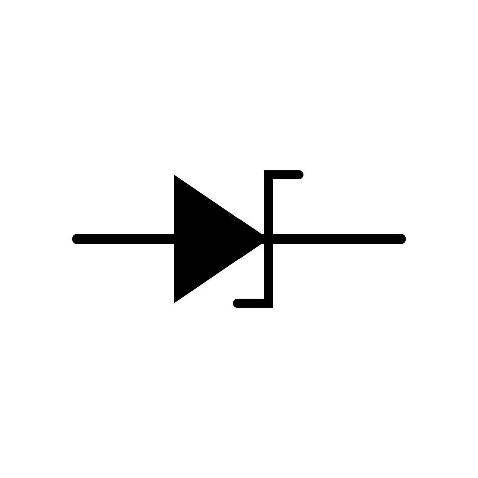
A Zener diode is a semiconductor device that allows current to flow forward like a regular diode but also in the reverse direction if the voltage is larger than the breakdown voltage, known as "Zener knee voltage" or "Zener voltage". This dual-directional functionality is the defining characteristic of Zener diodes and sets them apart from other diodes.
Zener diodes consist of a heavily doped P-N junction to reduce the breakdown voltage, which results in a thin depletion layer. The reduced breakdown voltage allows the diode to operate reliably in the reverse breakdown region without damaging the diode. This is a crucial characteristic of Zener diodes. It is a significant factor in their widespread use in various applications, particularly in voltage regulation tasks.
The name "Zener Diode" is derived from the Zener effect, named after Clarence Melvin Zener, who discovered this electrical phenomenon and led to the development and recognition of the Zener diode as an essential electronic component. However, it's worth noting that the operation of Zener diodes relies not only on the Zener effect but also on another phenomenon known as avalanche breakdown. Both these effects co-occur in a Zener diode but at different voltage levels. A Zener diode is a robust electronic component that can reliably operate in the reverse breakdown region, making it a valuable tool in many electronic circuits and systems. [1]
The Working Principle of Zener Diodes
The fundamental operation of a Zener diode hinges on a principle known as the Zener effect, which is a type of electrical breakdown. The Zener effect occurs in heavily doped diodes with a thin depletion layer. When a reverse voltage is applied to the diode and increased, a point is reached where the electric field enables the tunneling of electrons from the valence band to the conduction band, leading to a sudden increase in electric current. This voltage point is known as the Zener voltage, or Zener breakdown voltage.
The Zener diode is designed to have a reduced breakdown voltage, which means it can operate safely in the reverse breakdown region. When the applied reverse voltage reaches the Zener voltage, the diode allows a significant current to flow. However, even with an increase in current, the voltage across the diode remains stable at the Zener voltage, making it an excellent voltage regulator.
The Zener impedance is the equivalent series resistance of a Zener diode when conducting current. Ideally, it should be zero, but it has some impedance. Thus, a Zener diode acts as such only in a limited current range.
It's important to note that the Zener diode can also operate in the forward bias like a regular diode. In this mode, the diode allows current to flow when the forward voltage exceeds the forward voltage drop. However, the unique characteristic of the Zener diode is its ability to conduct in the reverse bias once the applied voltage reaches the Zener voltage, even though a small leakage current flows through the diode. [2]
Zener Breakdown: A Deep Dive
Unlike ordinary rectifier diodes, which are never intended to be operated at or near breakdown, a Zener diode is designed to operate in the breakdown region. Zener breakdown is a phenomenon that occurs in a Zener diode when the reverse bias voltage applied across it exceeds the Zener voltage. This breakdown is due to the intense electric field in the thin depletion region of the diode’s heavily doped P-N junction. The electric field is strong enough to pull electrons from their atomic orbits and add them to the free electron pool, leading to a significant increase in current.
The Zener or the reverse breakdown voltage is a critical parameter of a Zener diode. It is set during manufacturing by controlling the doping level. It typically ranges from 2.4 to about 200 volts for commercially available diodes. Once the breakdown occurs, the voltage across the diode remains almost constant, regardless of the change in current. This characteristic is the basis for using Zener diodes in voltage regulation applications.
The Zener breakdown is a quantum mechanical effect and is temperature-independent. However, in real-world applications, the Zener diode operates with a combination of Zener breakdown and another phenomenon known as avalanche breakdown. The avalanche breakdown is a thermally induced breakdown mechanism that dominates at higher breakdown voltages. [2]
Avalanche Breakdown vs Zener Breakdown
Avalanche breakdown and Zener breakdown are two distinct mechanisms that lead to the breakdown of a diode in reverse bias. Both phenomena result in a sharp increase in current. Still, they occur under different conditions and are driven by different physical principles.
Avalanche breakdown occurs in lightly doped diodes that have a thick depletion layer. When the reverse-bias voltage increases, the electric field becomes strong enough to accelerate free electrons to energies sufficient to ionize other atoms when they collide, creating more free electrons and holes. This process leads to an avalanche of charge carriers and a sudden increase in current. The avalanche breakdown is a thermally induced process and is temperature-dependent. The breakdown voltage increases with increasing temperature.
On the other hand, Zener breakdown occurs in heavily doped diodes with a thin depletion layer. The intense electric field in the depletion region pulls electrons from the valence band to the conduction band, leading to a significant increase in current. The Zener breakdown is a quantum mechanical effect and is mainly temperature-independent. The breakdown voltage decreases slightly with increasing temperature.
In practice, avalanche and Zener breakdown can occur in a Zener diode. For Zener diodes with a breakdown voltage below 5V, the Zener effect is dominant. In contrast, for those with a breakdown voltage above 5V, the avalanche effect becomes significant.
Avalanche breakdown and Zener breakdown are two distinct mechanisms that lead to the breakdown of a diode in reverse bias. Both phenomena result in a sharp increase in current. Still, they occur under different conditions and are driven by different physical principles.
Avalanche breakdown occurs in lightly doped diodes that have a thick depletion layer. When the reverse-bias voltage increases, the electric field becomes strong enough to accelerate free electrons to energies sufficient to ionize other atoms when they collide, creating more free electrons and holes. This process leads to an avalanche of charge carriers and a sudden increase in current. The avalanche breakdown is a thermally induced process and is temperature-dependent. The breakdown voltage increases with increasing temperature.
On the other hand, Zener breakdown occurs in heavily doped diodes with a thin depletion layer. The intense electric field in the depletion region pulls electrons from the valence band to the conduction band, leading to a significant increase in current. The Zener breakdown is a quantum mechanical effect and is mainly temperature-independent. The breakdown voltage decreases slightly with increasing temperature.
In practice, avalanche and Zener breakdown can occur in a Zener diode. For Zener diodes with a breakdown voltage below 5V, the Zener effect is dominant. In contrast, for those with a breakdown voltage above 5V, the avalanche effect becomes significant. [3]
Reading Recommendation: Optimizing Diode Functionality: Forward and Reverse Bias.
Zener Diode Characteristics
Zener diodes have several key characteristics that define their operation and application. One of the most important is the Zener voltage (Vz), the reverse voltage at which the Zener breakdown occurs. This voltage is set during manufacturing by controlling the doping level. It typically ranges from 2.4 to about 200 volts for commercially available diodes. The Zener voltage is a critical parameter for the diode's application in voltage regulation.
Another essential characteristic is the Zener test current (Iz), which is the current through the diode when the applied reverse voltage equals the Zener voltage. The test current validates the Zener voltage during manufacturing. Depending on the diode's power rating and intended application, it can vary.
Zener diodes also have a maximum power dissipation rating (Pz), the maximum power the diode can dissipate without exceeding its maximum junction temperature. Exceeding this rating can lead to thermal runaway. In this condition, the diode's temperature and current increase exponentially, destroying the diode.
The Zener resistance (Rz) is another crucial characteristic. It is the dynamic resistance of the diode in the breakdown region. It is calculated as the slight change in voltage (∆Vz) divided by the corresponding small change in current (∆Iz). The Zener resistance is typically low for Zener diodes with a higher breakdown voltage and higher for those with a lower breakdown voltage.
The maximum current (reverse) that a Zener diode can allow to flow through it when it is reverse-biased and operating in the Zener breakdown region. It is essential to consider it, especially in applications where the diode may be exposed to transient overvoltage conditions. [4]
Voltage-Current Characteristics
The voltage-current characteristics of a Zener diode are represented graphically by a curve known as the V-I characteristic curve. This curve shows the relationship between the voltage across the diode (V) and the current through the diode (I).
The Zener diode behaves like a regular diode in the forward bias region. The current increases exponentially with the voltage once the voltage exceeds the forward voltage drop (typically around 0.7V for silicon diodes).
The current in the reverse bias region remains almost zero until the applied voltage reaches the Zener voltage. The diode enters the breakdown region at this point, and the current increases dramatically. At the same time, the voltage remains nearly constant at the Zener voltage. This region is where the Zener diode operates in most of its applications.
The knee of the curve represents the Zener voltage, and the curve's steepness in the breakdown region represents the Zener resistance. The flatter the curve, the lower the Zener resistance, and the better the diode maintains a constant voltage.
Temperature Coefficient
The temperature coefficient of a Zener diode is a measure of how the Zener voltage changes with temperature. It is typically expressed in millivolts per degree Celsius (mV/°C) or as a percentage change per degree Celsius (%/°C). The temperature coefficient is an important parameter to consider when designing electronic circuits that involve Zener diodes, as it can affect the stability of the voltage regulation.
The temperature coefficient is usually harmful for Zener diodes with a breakdown voltage below 5V, meaning that the Zener voltage decreases as the temperature increases. This is due to the dominance of the Zener effect in these diodes, a quantum mechanical process that is mainly temperature-independent. However, the overall temperature coefficient is influenced by other factors, such as the diode's doping concentration and the presence of impurities.
In contrast, Zener diodes with a breakdown voltage above 5V typically have a positive temperature coefficient, meaning that the Zener voltage increases as the temperature increases. This is because the avalanche effect becomes dominant at higher breakdown voltages, and this effect is thermally induced and temperature dependent.
The temperature coefficient can vary significantly between Zener diodes, even those with similar breakdown voltages. Therefore, it is essential to consult the manufacturer's datasheet to obtain accurate temperature coefficient values for a specific diode. In some applications, it may be necessary to use temperature-compensated Zener diodes or other techniques to maintain a stable voltage regulation over a wide temperature range.
Reading Recommendation: Forward Bias, Reverse Bias and their effects on Diodes.
Zener Diode Models
Zener diode models are mathematical representations that describe the behavior of a Zener diode in a circuit. These models are used in circuit analysis and design to predict the performance of circuits that include Zener diodes. There are several models for Zener diodes, each with varying levels of complexity and accuracy.
The simplest model is the ideal Zener diode model, which assumes that the diode is either in the on-state or the off-state. In the on state, the diode is assumed to have zero resistance. In contrast, it is assumed to have infinite resistance in the off state. This model is helpful for basic circuit analysis but does not accurately represent the real-world behavior of a Zener diode.
More complex models consider the non-ideal characteristics of a Zener diode, such as its forward voltage drop, Zener resistance, and temperature coefficient. These models use mathematical equations to describe the voltage-current relationship of the diode. They can provide a more accurate prediction of the diode's behavior in a circuit. However, they are also more complex and require more computational resources. [3]
Ideal Zener Diode Model
The ideal Zener diode model is a simplified representation that assumes the diode has only two states: on and off. In the on state, the diode is assumed to have zero resistance, allowing current to flow freely. This state corresponds to the forward bias condition when the applied voltage is greater than the forward voltage drop and the reverse bias condition when the applied voltage is greater than the Zener voltage.
In the off state, the diode is assumed to have infinite resistance, blocking all current flow. This state corresponds to the reverse bias condition when the applied voltage exceeds the Zener voltage.
The ideal Zener diode model is helpful for basic circuit analysis and design, as it simplifies the behavior of the diode into two distinct states. However, it does not accurately represent the real-world behavior of a Zener diode, as it ignores several important characteristics, such as the forward voltage drop, Zener resistance, and temperature effects. Despite its limitations, the ideal Zener diode model provides a valuable starting point for understanding the operation of Zener diodes and their application in electronic circuits.
Practical Zener Diode Model
The practical Zener diode model is a more accurate representation of a Zener diode's real-world behavior than the ideal model. This model considers several non-ideal characteristics of the diode, such as the forward voltage drop, Zener resistance, and temperature effects.
The practical model considers the forward voltage drop when the diode is in the forward bias condition. This voltage drop is typically around 0.7V for silicon diodes and is not negligible, as assumed in the ideal model. Accounting for the forward voltage drop provides a more accurate prediction of the diode's behavior in a circuit.
Zener resistance is another essential factor to consider in the practical model. The diode in the reverse breakdown region does not maintain a perfectly constant voltage as assumed in the ideal model. Instead, the voltage across the diode varies slightly with changes in current due to the Zener resistance. The practical model uses the Zener resistance to describe this variation, providing a more accurate representation of the diode's behavior in the breakdown region.
Temperature effects are also considered in the practical Zener diode model. The Zener voltage and other parameters of the diode can change with temperature, affecting the performance of the diode in a circuit. The practical model considers the diode's temperature coefficient, allowing for a more accurate prediction of the diode's behavior over a range of temperatures.
The practical Zener diode model is more complex than the ideal model. Still, it provides a more accurate representation of the diode's behavior in real-world applications. By considering the non-ideal characteristics of the diode, the practical model allows engineers to design and analyze electronic circuits with greater precision and confidence.
Applications of Zener Diodes
Zener diodes are versatile electronic components with a wide range of applications due to their unique characteristics, such as maintaining a constant voltage in the reverse breakdown region. Zener diodes' most common applications include voltage regulation, waveform clipping, and transient voltage suppression.
Zener diodes can trigger specific actions in switching applications when a certain voltage level is reached. For example, they can be used as a voltage reference to turn on or off a transistor or an electronic switch at a predetermined voltage threshold. Moreover, in applications such as converters, zener diodes may occasionally produce electrical noise on the DC voltage supply as they work to steady the voltage. This is fine in most applications, but adding a high-value decoupling capacitor to the output of the diode can rectify the problem by providing extra smoothing. [4]
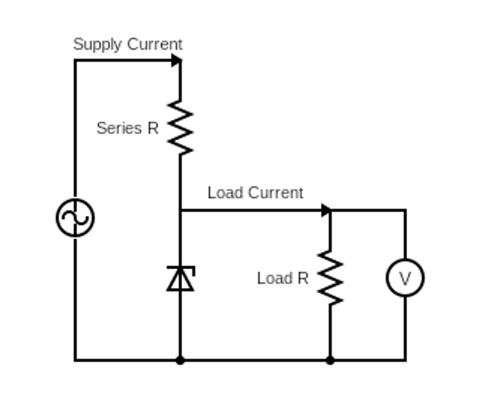
Voltage Regulation
One of the primary applications of Zener diodes is voltage regulation. In this application, the Zener diode is connected in parallel with the load, and it maintains a constant output voltage across the load, regardless of variations in the input voltage or load current. This is possible due to the diode's ability to maintain a stable voltage across its terminals in the reverse breakdown region.
When the input voltage is below the Zener voltage, the diode remains in the off state, and the output voltage is equal to the input voltage. However, when the input voltage exceeds the Zener voltage, the diode enters the breakdown region, and the voltage across the diode remains constant at the Zener voltage. This constant voltage is applied to the load, ensuring a stable output voltage.
To design a voltage regulator using a Zener diode, selecting a diode with the appropriate Zener voltage and power rating for the desired output voltage and load current is essential. Additionally, a series resistor is often used to limit the diode's current and ensure that it operates within its specified power dissipation limits.
Voltage regulation using Zener diodes is a simple and cost-effective solution for maintaining a stable output voltage in electronic circuits. However, it is essential to note that this method may not be suitable for applications requiring high precision or efficiency, as the Zener diode's characteristics can be influenced by factors such as temperature and manufacturing variations.
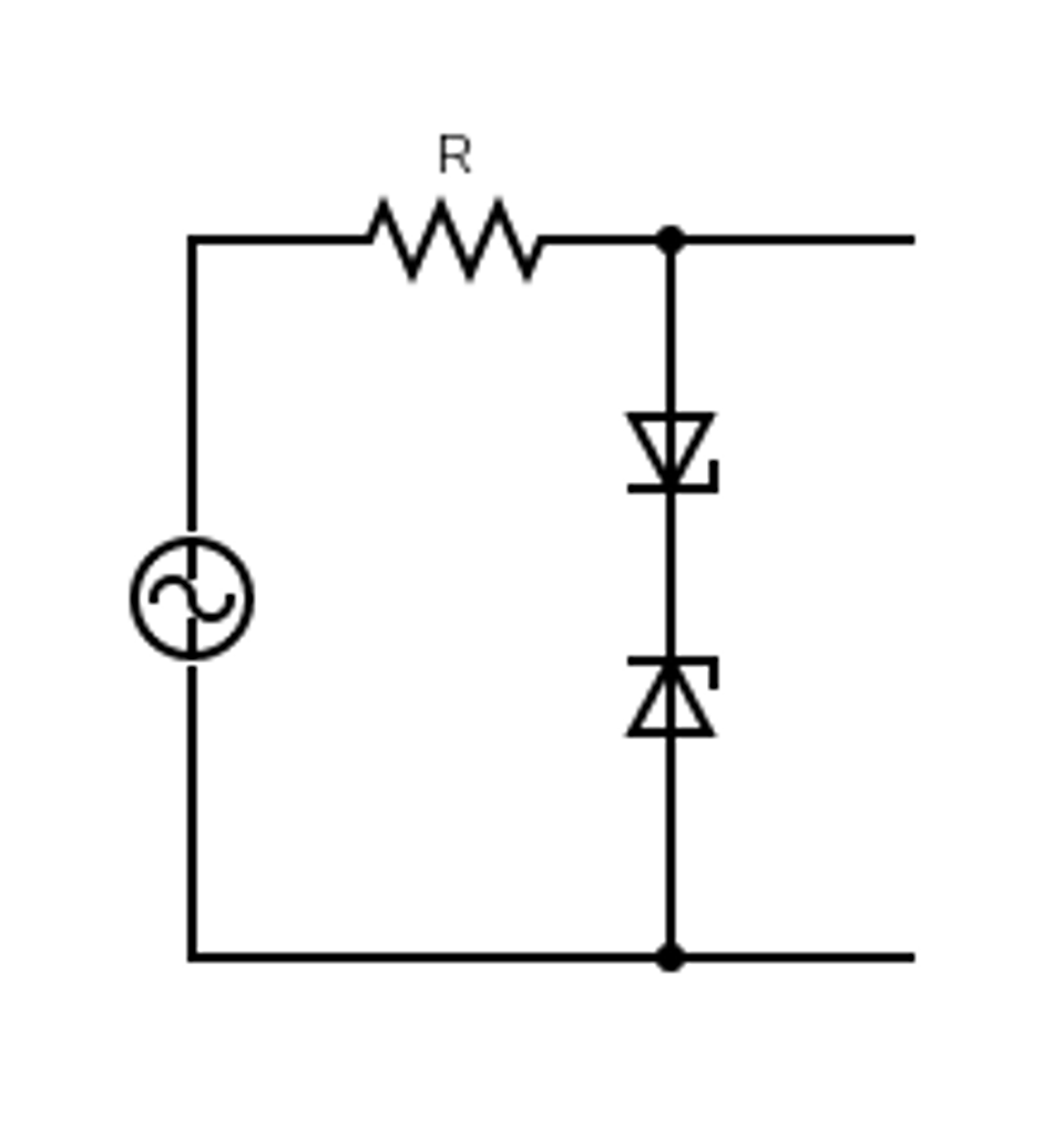
Waveform Clipping
Waveform clipping is another common application of Zener diodes. In this application, the diode shapes or modifies an input signal waveform by limiting its amplitude to a specific level. This can be useful in various scenarios, such as protecting sensitive electronic components from voltage spikes or generating specific waveform shapes for signal processing tasks.
The Zener diode is connected in series in a clipper circuit with the input signal and a load resistor. When the input signal voltage is below the Zener voltage, the diode remains in the off state, and the output waveform follows the input waveform. However, when the input signal voltage exceeds the Zener voltage, the diode enters the breakdown region, and the voltage across the diode remains constant at the Zener voltage. This limits the output waveform amplitude to the Zener voltage, resulting in a clipped waveform.
There are two types of clipping circuits: positive and negative. In a positive clipping circuit, the Zener diode is connected in reverse bias, and the output waveform is clipped at the Zener voltage level. In a negative clipping circuit, the diode is connected in forward bias, and the output waveform is clipped at the forward voltage drop level (typically around 0.7V for silicon diodes).
Selecting a Zener diode with the appropriate Zener voltage and connecting it in the desired configuration makes it possible to design waveform clipping circuits that meet specific requirements for amplitude limitation and waveform shaping. This versatile application of Zener diodes is widely used in various electronic systems, such as audio processing, communication systems, and power supply protection.
In the example below, the circuit can clip the waveform between a positive value of +8.2V and a negative value of -8.2V for a 7.5V zener diode. This type of clipper configuration is common for protecting an electronic circuit from overvoltage.
Reading Recommendation: Revolutionizing Drone Production with 3D Printing.
Conclusion
Zener diodes are a fundamental component in many electronic circuits, offering unique characteristics such as a stable voltage in the reverse breakdown region. This property is leveraged in various applications, including voltage regulation and waveform clipping. Understanding the behavior of Zener diodes in ideal and practical models is crucial for designing and analyzing electronic circuits. While the ideal model offers a simplified view of the diode's operation, the practical model provides:
A more accurate representation.
Accounting for real-world factors such as forward voltage drop.
Zener resistance.
Temperature effects.
Despite their simplicity, Zener diodes play a critical role in the functionality and reliability of many electronic systems.
Frequently Asked Questions (FAQs)
What is a Zener diode?
A Zener diode is a type of diode that allows current to flow not only from its anode to its cathode, but also in the reverse direction when the Zener voltage is reached.
What is the Zener voltage?
The Zener voltage is the voltage at which the diode breaks down and allows current to flow in the reverse direction. This is a characteristic property of the diode and is determined during manufacturing.
What is the temperature coefficient of a Zener diode?
The temperature coefficient of a Zener diode is a measure of how the Zener voltage changes with temperature. It is typically expressed in millivolts per degree Celsius (mV/°C) or as a percentage change per degree Celsius (%/°C).
What is the difference between the ideal and practical Zener diode models?
The ideal Zener diode model simplifies the diode's behavior into two states: on and off. The practical model, on the other hand, takes into account several non-ideal characteristics of the diode, such as the forward voltage drop, Zener resistance, and temperature effects.
What are some applications of Zener diodes?
Zener diodes are commonly used in voltage regulation, waveform clipping, and transient voltage suppression. In voltage regulation, the diode maintains a constant output voltage across a load. In waveform clipping, the diode limits the amplitude of an input signal to a specific level. In transient voltage suppression, the diode protects sensitive components from voltage spikes.
References
Electronic Notes. “Zener Diode Invention & History”
TTI Inc. “What is a Zener Diode?”
RS Components Ltd. “A Complete Guide to Zener Diodes”
Electronics Tutorial. “The Zener Diode”