Enhancement vs Depletion MOSFETs: Design, Applications & Future Trends
Enhancement-mode and depletion-mode MOSFETs are types of field-effect transistors with opposite default states—normally off vs. normally on. This guide breaks down their behavior, biases, equations, real-world uses, and 2025 tech trends.

23 Jul, 2025. 26 minutes read

Introduction
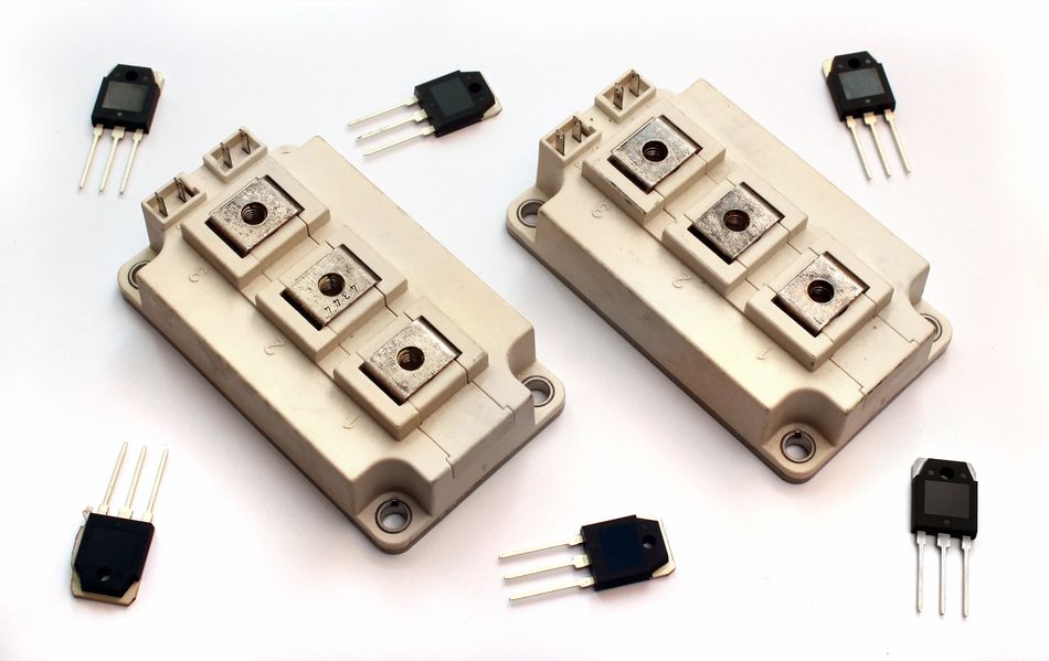
In the world of modern electronics, MOSFETs—short for Metal-Oxide Semiconductor Field Effect Transistors—are essential building blocks. Among them, two major types stand out: enhancement-mode and depletion-mode MOSFETs. These devices differ fundamentally in their default behavior. An enhancement-mode MOSFET remains off until a gate-source voltage (VGS) exceeds its threshold voltage (VTH), creating a conductive channel. In contrast, a depletion-mode MOSFET conducts when VGS is zero and requires reverse bias to switch off, functioning much like a JFET.
Understanding these operational modes helps engineers design better circuits across various applications—from switching regulators and inverters to amplifiers, current regulators, and analog signal paths. Whether you're working with n-channel enhancement-mode MOSFETs for high-speed switching or leveraging p-channel depletion devices for fail-safe biasing, knowing the right device and how to bias it properly can dramatically improve reliability, efficiency, and safety. Choosing the correct gate voltage, anticipating leakage current, and accounting for conduction losses all start with understanding the MOSFET's mode of operation.
Theoretical foundations reveal enhancement vs depletion MOSFET differences
In 2025, high-efficiency power and signal electronics rely heavily on selecting the right type of MOSFET. Understanding the theoretical foundation behind enhancement-mode and depletion-mode MOSFETs reveals why one is normally off and the other normally on. At the core, both devices are field effect transistors (FETs), using an electric field at the gate terminal to control the conductivity of a semiconductor channel between the source terminal and the drain.
In an enhancement-mode MOSFET, the channel doesn’t exist at rest. When VGS (gate-source voltage) is zero, there is no conduction, especially in n-channel enhancement types like NMOS, which require a positive gate voltage above the threshold voltage (VTH) to create a conductive path for electrons. The result is a transistor that behaves like a normally open switch, conducting only when deliberately turned on. This makes enhancement-mode MOSFETs ideal for logic circuits and fail-safe power systems. Their behavior can be modeled by the quadratic relation:
ID ≈ k(VGS – VTH)²,
where ID is the drain current and k is the device constant.
By contrast, a depletion-mode MOSFET—often compared to a JFET or a depletion-mode device—has a pre-formed channel that conducts when VGS = 0. These devices are normally on, and to turn them off, the gate must be driven below the cut-off point. For an n-channel depletion-mode MOSFET, a negative gate voltage reduces the number of free electrons in the channel, pushing the device toward non-conduction. This behavior is modeled by:
ID = IDSS(1 – VGS / VGS(off )²,
where IDSS is the saturation drain current at zero bias and VGS(off) is the cutoff voltage.
P-channel MOSFETs, both enhancement and depletion types, behave similarly but with reversed polarities. A PMOS enhancement device turns on with a negative VGS, while a p-channel depletion MOSFET requires a positive gate voltage to turn off. Though less common in depletion form, they remain useful in analog or current-limiting roles. Whether n-type or p-type, the distinction between enhancement and depletion modes ultimately lies in the default conduction state and how gate voltage modulates the channel's charge carriers.
Recommended reading: How Do MOSFETs Work: Comprehensive Technical Guide for Engineers (2025)
Analysis techniques leverage biasing and threshold characterization
To design effective circuits using MOSFETs, engineers must go beyond mode classification and dive into the core of how these devices operate under varying voltage conditions. Three key analysis techniques dominate modern electronic design: identifying MOSFET type from datasheets, applying appropriate biasing strategies for enhancement-mode devices, and managing current flow in depletion-mode devices through reverse gate biasing.
1. Identifying the MOSFET Type from Datasheet Characteristics
The first step in any MOSFET-based design is determining whether the device is enhancement-mode or depletion-mode, and this begins with the datasheet. For enhancement-mode devices, the threshold voltage (VTH) is positive for n-channel MOSFETs (NMOS) and negative for p-channel MOSFETs (PMOS). This threshold indicates the minimum gate-source voltage (VGS) required to turn the device on. In contrast, depletion-mode MOSFETs specify a cut-off voltage often labeled as VGS(off). For n-channel depletion-mode MOSFETs, this value is typically between –2 V and –5 V, indicating that the device conducts at VGS = 0 and must be reverse-biased to stop conduction.
To verify this from the datasheet, engineers examine transfer characteristic curves (ID vs. VGS), which show how drain current behaves across gate voltages. A depletion-mode MOSFET will display significant current at VGS = 0, while an enhancement-mode device remains non-conductive below its threshold. Moreover, simulation libraries like SPICE models often include parameters such as VTO (threshold voltage) and IDSS (saturation current at VGS = 0), which further clarify a MOSFET's behavior. Recognizing these identifiers early on prevents misapplication and ensures proper circuit function.
2. Biasing Enhancement-Mode MOSFETs for Accurate Turn-On Behavior
Once an enhancement-mode device is identified, proper biasing becomes essential. These MOSFETs are normally off and require a gate-source voltage (VGS) greater than VTH to conduct. The relationship between gate voltage and drain current (ID) in the saturation region is given by the equation:
ID = ½ × k × (VGS – VTH)²,
where k is a device-specific transconductance constant derived from the channel length, mobility, and oxide capacitance.
In practical terms, if a designer wants a drain current of 50 mA and the MOSFET’s VTH is 2 V with k = 0.02 A/V², the required VGS becomes approximately 4.24 V. Biasing circuits may use a resistive divider, a gate driver IC, or a regulated power rail to achieve this voltage. It's crucial to remember that VGS = VG – VS, so in high-side switching, special attention must be given to the source terminal potential. Engineers often place a resistor (10–100 Ω) at the gate terminal to limit inrush current during switching and prevent high-frequency oscillation. Biasing is especially important in CMOS logic applications, where n-channel and p-channel enhancement-mode MOSFETs form the basis of digital inverters and logic gates.
3. Biasing Depletion-Mode MOSFETs for Controlled Conduction
In contrast to enhancement-mode devices, depletion-mode MOSFETs are normally on, and engineers must use reverse bias to limit or stop conduction. These devices follow a different current equation:
ID = IDSS × (1 – VGS / VGS(off))²,
where IDSS is the drain current at VGS = 0 and VGS(off) is the voltage at which the MOSFET ceases to conduct. For example, if IDSS is 5 mA and VGS(off) is –3 V, setting VGS to –1.5 V yields a controlled ID of 1.25 mA. This predictable relationship allows designers to treat the device like a JFET or use it in analog biasing roles.
One effective method is self-biasing using a source resistor. If 2 mA flows through a 1 kΩ resistor at the source, a –2 V gate-to-source drop is created, reducing current. In simpler designs, engineers tie the gate terminal directly to the drain, forming a two-terminal current regulator that stabilizes current flow automatically. These configurations are popular in LED drivers, startup biasing for power supplies, and low-noise analog circuits. Unlike enhancement-mode devices, depletion-mode MOSFETs offer constant current control with minimal external components. However, engineers must always account for leakage current, thermal drift, and impedance variations that may shift the actual cut-off point over time or temperature.
Recommended reading: How to Test a MOSFET: Theoretical Basics and Practical Step-by-Step Guide
Bold Key Metrics: Enhancement vs Depletion Biasing
Metric / Term | Enhancement-Mode MOSFET | Depletion-Mode MOSFET |
Default State (VGS = 0) | OFF (No conduction) | ON (Full conduction) |
Turn-On Requirement | VGS > VTH | VGS < VGS(off) |
Threshold Voltage (VTH) | Positive (NMOS), Negative (PMOS) | Defined by VGS(off), typically –2 V to –5 V |
Biasing Strategy | Apply forward VGS (gate above source) | Apply reverse VGS (gate below source) |
Conduction Equation | ID = ½ × k × (VGS – VTH)² | ID = IDSS(1 – VGS / VGS(off))² |
Typical Applications | Logic gates, switches, and amplifiers | Current regulators, startup bias, and analog loads |
Common Devices | IRF540N, 2N7000, BS170 | DN2540, J176, BSS100 |
Simulation Flags | Check for VTO or LEVEL 3 model | Ensure IDSS and VGS(off) are specified |
Common Applications Span from Power Converters to Analog Circuits
From low-power logic circuits to high-efficiency power systems, the use of MOSFETs—both enhancement-mode and depletion-mode—spans nearly every domain of modern electronics. Below are four major application areas that highlight how different types of MOSFETs, including n-channel, p-channel, and depletion-type devices, are used for performance, safety, and control.
1. Power Converters and High-Frequency Switching
Enhancement-mode n-channel MOSFETs dominate in switch-mode power supplies (SMPS), DC-DC converters, and motor controllers due to their low RDS(on) and high-speed switching capabilities. These devices are typically used in buck, boost, or synchronous rectifier topologies, where they rapidly toggle between cut-off and saturation to modulate output voltage and current flow. Controlled by dedicated gate drivers, they operate efficiently at high frequencies, minimizing power loss and heat. The threshold voltage (VTH) must be carefully selected to match the system’s gate drive voltage, ensuring full enhancement with minimal conduction resistance.
P-channel MOSFETs, though less common in high-current switching, serve a niche in high-side switching applications. Their ability to turn on with a negative VGS simplifies the drive circuitry when using a single power rail. However, their higher on-resistance, due to lower hole mobility in the p-type substrate, limits their use in high-power designs. They remain valuable where PCB layout simplicity or fault isolation is prioritized.
2. Analog Circuits and Precision Amplifiers
In analog signal paths, MOSFETs offer excellent performance due to their high input impedance, low gate leakage current, and precise biasing capability. Enhancement-mode MOSFETs are used in voltage amplifiers, active loads, and source followers. Their voltage-controlled behavior allows for linear operation with minimal distortion. A well-designed bias network, often involving resistors and sometimes capacitors, positions the gate voltage above VTH, ensuring the device operates in the desired region (saturation or triode).
Depletion-mode MOSFETs, functioning like JFETs, are ideal for analog constant-current sources, bias stabilization, and low-noise amplifier stages. Their ability to conduct at VGS = 0 makes them useful as self-biasing current sinks. In analog filters or differential pairs, this consistent current improves gain and signal linearity. Their inclusion in discrete op-amp designs or instrumentation-grade front-ends shows their value in precision electronics.
3. Digital Logic and CMOS Integration
CMOS (Complementary MOSFET) technology combines n-channel enhancement-mode MOSFETs (NMOS) and p-channel enhancement-mode MOSFETs (PMOS) in a push-pull configuration. This pairing allows digital gates like inverters, NANDs, and NORs to achieve near-zero static power consumption, since one device is always off when the other is on. In this arrangement, precise threshold voltages, carefully controlled substrate doping, and minimal leakage current are critical to ensure reliable switching, especially at nanometer scales in VLSI.
Because CMOS circuits rely on the rapid alternation between conduction and cut-off, MOSFETs are chosen for their fast switching characteristics and low gate capacitance. Logic-level devices often have lower VTH values to accommodate 3.3V or 1.8V logic levels, as found in microcontrollers, memory arrays, and integrated systems-on-chip. Here, small parasitics, including gate-to-source capacitance, can affect timing and are often modeled in SPICE simulations.
4. Startup Circuits, Current Regulators, and Passive Controls
In power supply startup and current-regulation applications, depletion-mode MOSFETs excel. Their normally-on behavior allows them to supply an initial bias current to controllers or regulators during power-up sequences. Once downstream control circuitry is active, these MOSFETs can be turned off by pulling the gate voltage negative relative to the source terminal, avoiding the need for high-wattage startup resistors.
They also serve as two-terminal current regulators by simply connecting the gate terminal to the drain, allowing a self-limiting drain current set by a source resistor. This is ideal for LED drivers, biasing RF amplifiers, or forming passive current sources in analog loops. The simplicity of these configurations reduces part count while improving reliability in space-constrained designs like IoT sensors or industrial controllers.
In these applications, careful consideration of leakage current, VGS(off), and thermal drift is essential, as misjudging the cut-off behavior can lead to circuit instability or component stress. Nonetheless, depletion-mode devices remain unmatched for passive, low-power current control with minimal complexity.
Recommended reading: JFET vs MOSFET: A Comprehensive Engineering Analysis and Selection Guide
Integration with GaN technology enables high-speed, high-efficiency power systems
As the demand for higher power density and faster switching increases across industries, Gallium Nitride (GaN) has emerged as a transformative material in semiconductor technology. When paired with traditional MOSFET architecture, particularly enhancement-mode n-channel MOSFETs, GaN enables the creation of ultra-efficient, high-frequency power systems capable of outperforming silicon-based devices in nearly every metric.
1. Why GaN Outperforms Traditional Silicon MOSFETs
GaN devices offer several advantages over conventional silicon MOSFETs: higher electron mobility, wider bandgap, and greater breakdown voltage. These characteristics translate to faster switching speeds, reduced gate charge, and significantly lower conduction and switching losses. In practice, this allows GaN-based enhancement-mode MOSFETs to operate at switching frequencies above 1 MHz, which reduces the size of external passive components like capacitors and inductors in power converter designs.
Unlike traditional depletion-mode GaN FETs, modern systems use enhancement-mode GaN HEMTs (High Electron Mobility Transistors) that behave much like n-channel MOSFETs. These devices are normally off, requiring a positive gate-source voltage (VGS) to turn on, making them safer and easier to control in high-speed digital and analog circuits. Engineers can apply the same biasing techniques used in silicon enhancement-mode MOSFETs, though special attention must be given to gate voltage overshoot, impedance matching, and thermal design due to GaN's unique characteristics.
2. Gate Drive and Biasing Challenges with GaN
One of the critical considerations when integrating GaN devices is gate drive design. GaN transistors typically operate with lower threshold voltages (e.g., 1.5 V to 2.5 V), and are highly sensitive to gate voltage overshoot or noise. Even brief excursions beyond their rated VGS(max)—often just ±6 V—can lead to leakage current, degradation, or failure.
Designers use specialized gate drivers with precise rise and fall time control, tight voltage regulation, and often include active gate clamp circuitry to protect the gate terminal. Unlike traditional MOSFETs, where a simple resistor may suffice, GaN gate drive circuits often require matched impedance and low-inductance PCB traces to avoid ringing and parasitic conduction. Gate-source capacitance, while low, must still be accounted for during high-speed transitions.
In many circuits, GaN-based n-channel enhancement-mode devices are replacing silicon MOSFETs in half-bridge, totem-pole PFC, and isolated DC-DC topologies. Some systems still use depletion-mode GaN FETs in auxiliary functions like startup biasing, but these are gradually being phased out due to control complexity.
3. Real-World Applications and Performance Gains
The integration of GaN-based enhancement-type MOSFETs has dramatically improved the efficiency and form factor of modern electronics. In power supply units for laptops, electric vehicles, telecom base stations, and data centers, GaN circuits deliver faster transient response, higher power density, and lower thermal losses. A traditional 500 kHz buck converter using silicon can often be replaced with a 2 MHz GaN converter, cutting down capacitor and inductor sizes by more than half.
For applications like wireless charging, Class D audio amplifiers, or fast USB-C PD chargers, GaN-based field effect transistors enable sleeker, lighter, and more efficient designs. When combined with advanced biasing and threshold control, these devices outperform BJTs, JFETs, and standard MOSFETs, redefining what’s possible in compact power systems.
Designers must still be mindful of integration details, including thermal impedance, substrate layout, and electromagnetic interference (EMI). But with the right approach, GaN is not just a replacement for silicon—it’s a leap forward.
Modern software tools revolutionize MOSFET mode implementation
Designing and implementing circuits with enhancement-mode or depletion-mode MOSFETs has been transformed by powerful modern software tools. In 2025, engineers will benefit from advanced simulation environments, AI-assisted design workflows, and intelligent PCB platforms that streamline everything from component selection to full-system optimization. These tools not only simulate MOSFET behavior with incredible accuracy but also help engineers visualize the impact of threshold voltage, VGS, and drain current across both analog and digital circuits. Here, we explore three key categories of tools and how they specifically address MOSFET mode implementation.
1. SPICE Simulation Tools for Circuit-Level Behavior
Traditional SPICE-based simulators remain the cornerstone of MOSFET circuit design, especially for switched-mode power supplies, analog amplifiers, and logic-level switching. Tools like LTspice (Analog Devices, 2023) and QSPICE (Qorvo, 2024) offer extensive model libraries that include both enhancement-mode and depletion-mode MOSFETs. These simulators allow users to run time-domain, DC sweep, and parametric simulations, making it possible to observe effects like the ID–VGS curve, threshold shifts, and conduction behavior at different temperatures or gate voltages.
Designers can directly compare how a +4 V vs –2 V VTH affects circuit operation, or simulate how leakage current, RDS(on), and gate capacitance behave under thermal stress. LTspice is widely used for power circuits due to its robust convergence and community support, while QSPICE brings optimized models for GaN devices and better support for RF/power integration. Both support advanced modeling of temperature effects, critical for applications where threshold voltage and on-resistance vary with thermal load.
2. TCAD Tools for Semiconductor-Level Analysis
For semiconductor professionals and research engineers, TCAD (Technology Computer-Aided Design) tools like Synopsys Sentaurus (2025) and Silvaco ATLAS (v.2024) enable deep, physics-based simulation of MOSFET structures. These platforms allow users to virtually dope a substrate, apply implant profiles, and simulate resulting band diagrams, enabling precise control over whether a device functions in enhancement or depletion mode.
For example, adding an N-channel implant to a lightly doped region can yield a depletion-mode MOSFET, with a simulated VTH of –1.5 V, whereas a lower doping profile may result in an enhancement-mode MOSFET with a VTH of +0.7 V. These tools are indispensable in ASIC development, novel transistor research, and custom IC design, where standard models don’t apply. While TCAD is rarely used in day-to-day circuit design, its ability to simulate carrier mobility, channel depth, and substrate effects makes it critical for advanced R&D in semiconductor manufacturing.
3. PCB and Circuit Design Tools for Practical Implementation
Design tools like Altium Designer (2025) and Cadence OrCAD (17.4) bring MOSFET mode awareness directly into the schematic and layout environment. These platforms now include rule-checking features and component libraries that alert designers to the unique requirements of certain MOSFET types. For instance, placing a depletion-mode n-channel MOSFET may trigger a warning such as “Requires negative gate bias – ensure gate driver is configured.” This avoids design oversights that could result in unsafe or non-functional systems.
Moreover, these tools integrate with SPICE simulators, allowing users to simulate subcircuits directly from a schematic by selecting a component and launching a transient or AC analysis. Their internal libraries often recognize parts like DN2540, BSS139, and J176, complete with application notes, footprints, and thermal specifications, making component selection and board-level integration faster and more accurate. This synergy between symbol recognition, footprint placement, and biasing awareness is especially valuable when working with rare MOSFET variants, mixed-mode circuits, or custom gate driver setups.
4. Comparison of Top Tools
Below is a comparison of 5 common tools and their capabilities related to MOSFET design:
Tool (Developer, Year) | Primary Use | MOSFET Mode Support | Standout Feature |
LTspice XVII (ADI, 2023) | Circuit simulation (SPICE) | E-mode & some D-mode models | Robust MOSFET library and community examples |
QSPICE (Qorvo, 2024) | Circuit simulation (SPICE) | E-mode & GaN e/d-mode HEMTs | Fast mixed-signal sim, GaN focus |
Synopsys TCAD (Sentaurus 2025) | Device physics simulation | Custom mode (any doping) | Predictive device modeling (design your MOSFET) |
Altium Designer 24 (2024) | PCB design & schematics | Warnings for D-mode parts | Component library with mode notes |
Cadence PSpice/OrCAD 17.4 (2022) | Circuit sim & PCB design | E-mode default (D-mode via lib) | Integrated scheme-to-sim workflow |
Table: Comparison of software tools for designing with MOSFETs, highlighting how each handles enhancement (E-mode) and depletion (D-mode) device modeling. Bold features mark standout capabilities in 2025.
As shown, tools like LTspice and QSPICE excel in providing ready-to-use models and fast simulation for iterative circuit design, while TCAD offers deeper device-level exploration. PCB design suites help ensure nothing is overlooked when incorporating unusual devices like depletion-mode MOSFETs. By leveraging these modern tools, engineers can virtually prototype circuits in minutes, catching pitfalls (such as a depletion device left inadvertently conducting) before hardware build. This revolution in software support means implementing a mix of enhancement and depletion transistors is more accessible and reliable than ever before.
Best Practices Address Common Implementation Pitfalls
When working with enhancement-mode and depletion-mode MOSFETs, even experienced engineers can run into classic mistakes, leading to poor performance, circuit damage, or safety risks. With increasingly compact and high-speed designs, the stakes are higher than ever. Adopting the right MOSFET design practices and applying verification techniques early can prevent failures ranging from unexpected current flow to gate oxide breakdown. Below are five of the most common pitfalls and how to avoid them through smart design, simulation, and standards compliance.
1. Mistake: Using a Depletion MOSFET Without Proper Gate Bias
Problem: A common misconception is to treat a depletion-mode MOSFET like an enhancement device, assuming it's off by default. This often leads to circuits that are always on, because depletion-mode devices conduct when VGS = 0.
Solution: Always remember that depletion-mode MOSFETs are normally on. To turn them off, a proper gate-source bias (typically negative for n-channel) must be applied. For example, if using a DN2540, design a resistor network to apply a startup bias or use a timing circuit to ensure the gate voltage goes negative before applying high voltage across the drain and source. In safety-critical systems (IEC 61508), fail-safe biasing is often mandated when normally-on devices are used.
Verification: Run a SPICE simulation of the power-up sequence to confirm that VGS < VGS(off) within the required timeframe. On hardware, use an oscilloscope to measure VGS immediately after power-up to ensure the device is off when it should be.
2. Mistake: Misreading the Symbol and Assuming the Wrong Mode or Orientation
Problem: The MOSFET symbol varies subtly between enhancement and depletion modes. Designers sometimes misinterpret the solid line (used for depletion mode) as just a styling difference or forget to check the source/drain orientation.
Solution: Learn to read the symbols accurately. A solid channel line indicates a depletion-mode device, while a broken line is for enhancement mode. When unsure, always check the datasheet and confirm the threshold voltage (VTH) or VGS(off) value. Clearly label the mode in the schematic (e.g., “DN2540 (depletion)”) to avoid confusion.
Verification: Use a design checklist that includes verifying MOSFET mode and orientation. Simulation must also use the correct model type—an enhancement-mode SPICE model applied to a depletion part yields invalid results
3. Mistake: Driving the Gate with Inappropriate Voltage Levels
Problem: Applying incorrect gate voltage (VGS) can result in either incomplete turn-on, excessive RDS(on), or even gate oxide failure.
Solution: Match your gate driver to the MOSFET’s requirements. If the device needs 10 V for full turn-on but you’re using a 3.3 V signal, conduction will be poor and heating will occur. Conversely, applying –15 V to a depletion-mode gate rated for –5 V will rupture the gate oxide. Use level shifters or gate driver ICs rated for your device. In some cases, cascode configurations can allow indirect control of depletion-mode FETs with standard logic.
Verification: Bench-test VGS sweeps while monitoring drain current (ID) to ensure you're within safe limits. Check for ringing or overshoot with an oscilloscope—adding a small gate resistor can tame fast edges.
4. Mistake: Overlooking the Fail-Safe Risks of Normally-On Devices
Problem: If a depletion-mode MOSFET fails or loses its gate bias, it defaults to full conduction, which can lead to hazardous conditions, especially in power supplies or linear regulators.
Solution: Account for failure modes in design. Add a crowbar circuit, output clamp, or hardware interlock to prevent unsafe voltages. Alternatively, avoid depletion devices in systems where a default-on condition is unacceptable. Safety standards such as UL/IEC 60950 require that no single failure leads to a hazardous state.
Verification: Simulate loss-of-gate-drive scenarios. Use FMEA documentation to show how risks are mitigated, and include interlocks in your schematics where appropriate.
5. Mistake: Confusing Drain and Source in Depletion Applications
Problem: While enhancement-mode MOSFETs are often symmetrical, body diode direction and biasing assumptions make source/drain roles more critical in depletion-mode applications, especially in analog loads or current regulators.
Solution: Always follow the datasheet-recommended orientation. In topologies like high-side loads, the source terminal might be at a higher potential than the drain, depending on the function. Remember that body diodes conduct when reverse-biased incorrectly. For n-channel depletion-mode parts acting as loads, keeping the drain at a lower potential than the source ensures the diode does not conduct unintentionally.
Verification: Simulate DC bias points to ensure proper current direction and diode blocking. During layout reviews, verify the polarity of body diodes using part datasheets or SPICE models.
Engineers unlock the full potential of both enhancement and depletion-mode MOSFETs by addressing common mistakes early through simulation, documentation, and schematic clarity. Today’s precision requirements and tighter safety margins mean even small oversights become critical. In 2025, engineers don't just pick the right field-effect transistor; they implement it with discipline, foresight, and the help of robust tools and standards.
Recent Developments Push Boundaries of Transistor Technology
The world of transistors is advancing rapidly, and the lines between enhancement-mode and depletion-mode MOSFETs are beginning to blur. Breakthroughs from 2022 through 2025 are redefining what's possible—making exotic materials practical, designing transistors with switchable modes, and forming new industry standards to support innovation. These developments are shaping the future of power electronics, adaptive circuits, and semiconductor fabrication, while targeting key concerns like efficiency, safety, and threshold voltage control.
1. GaN and Wide-Bandgap Advances (2024–2025)
A major trend has been the transformation of normally-on GaN FETs into enhancement-mode devices to make them more suitable for commercial adoption. In early 2024, Cambridge GaN Devices introduced their H2 series GaN ICs that use standard-like gate drives, simplifying integration into existing control architectures. By late 2024, Transphorm released second-gen GaN FETs with gate injection transistors, allowing inherently normally-on structures to behave as enhancement-mode, while Efficient Power Conversion (EPC) launched e-mode GaN FETs capable of operating at high junction temperatures, a key milestone for EV and aerospace applications.
The Applied Power Electronics Conference (APEC) 2025 dedicated multiple sessions to gate driver techniques for enhancement-mode GaN devices. A key industry focus now is on reliability, ensuring these transistors remain off even under voltage spikes and transient events. Some are now qualified to sustain >700 V spikes without reverting to conduction, a critical benchmark for compliance in harsh environments.
2. Dual-Mode and Reconfigurable Transistors (2022–2025)
Research labs are pushing the boundaries with transistors that can toggle between enhancement and depletion mode based on bias or control input. In 2022, Nguyen-Dang et al. from UC Santa Barbara introduced an organic electrochemical transistor that could be set to either mode dynamically using conjugated polymers. These dual-mode devices represent a major step toward reconfigurable electronics—circuits that adapt their behavior in real time. Imagine a MOSFET that operates as normally-off in one moment and normally-on the next, depending on software input or system conditions.
By 2025, prototype logic gates and adaptive sensors are being built using this concept, with early applications in neuromorphic computing and space-grade electronics. The IEDM 2024 conference featured papers on polymorphic transistors, including an MIT study demonstrating silicon FinFETs with dynamically adjustable threshold voltage, allowing partial post-fabrication mode tuning.
3. Advanced Materials and New Device Structures (2023–2025)
Material innovation is driving the evolution of MOSFET characteristics. Researchers at Stanford in 2023 demonstrated a 2D material FET using MoS₂ with ambipolar conduction, capable of behaving near threshold neutrality (i.e., VTH ≈ 0 V). These devices blur the enhancement–depletion boundary, as they are “slightly on” at rest but become fully conductive with minor VGS changes, similar to depletion-mode behavior with enhancement-level control.
Another advancement is the rise of negative capacitance FETs (NC-FETs), which leverage ferroelectric materials to achieve subthreshold slopes below 60 mV/decade. Though these are technically enhancement-mode, their ultra-low turn-on requirements offer near-depletion functionality. TSMC and Intel are rumored to be evaluating NC-FETs for advanced nodes (targeting ~2027), but research activity in 2025 is already indicating that these may bring near-zero gate drive designs to CPUs and high-performance computing.
4. Industry Standards and Collaborative Innovation
To support these cutting-edge devices, the industry is adapting fast. In 2024, the JEDEC committee began drafting formal test procedures for depletion-mode power MOSFETs, especially focused on behavior when VGS = 0 or when the gate is tied to the source—cases previously underexplored in standard specs.
Simultaneously, the IEEE Power Electronics Society (2025) launched a working group on cascode GaN topologies, where depletion-mode and enhancement-mode MOSFETs are used together in hybrid packages. This move reflects increasing adoption of complex devices that combine the best of both worlds.
On the industry side, STMicroelectronics partnered with Exagan in 2023 to co-develop GaN-on-silicon enhancement-mode devices for compact power adapters. In 2024, ON Semiconductor introduced a family of “combo” FETs that package a depletion-mode startup FET and an enhancement-mode switching FET into one module, ideal for offline converters and industrial power supplies.
5. Looking Ahead: From Dichotomy to Design Spectrum
The era of viewing enhancement and depletion as binary modes is evolving. Between reconfigurable transistors, adaptive materials, and hybrid packaging strategies, the future is shifting toward a spectrum of tunable behaviors. Whether it's a MOSFET that nearly conducts at 0 V, or a transistor that changes mode based on software input, engineers in 2025 must think beyond static modes and embrace configurable architectures.
As this landscape continues to shift, the ability to understand and adapt to device-level behavior, gate biasing requirements, and threshold voltage engineering will be key. Designers must stay agile, leaning on simulation, standards, and collaboration to make the most of the new tools and technologies that challenge the old rules of FET design.
Recommended reading: Next-generation MOSFET technology Meets Demand for Strong Thermal Performance in Automotive Applications.
Advanced Techniques Reveal Sophisticated Applications
Beyond textbook applications, advanced engineers are using enhancement-mode and depletion-mode MOSFETs in highly innovative ways to solve complex challenges. These implementations often surface in cutting-edge research, aerospace, quantum computing, or high-performance analog and power electronics. Understanding the nuances of MOSFET operational modes unlocks a toolbox of strategies—some of which blur the boundaries between enhancement and depletion behavior. Below are four high-end examples showing how device-level mastery becomes a pathway to disruptive design.
Multi-Threshold CMOS and Adaptive Biasing
In modern IC design, the use of multi-threshold voltage (multi-Vt) transistors is a performance-power balancing act. Although all devices are typically enhancement-mode, designers intentionally vary threshold voltage (VTH) across the chip. “Low-Vt” transistors behave almost partially on at VGS = 0 (leakier, but faster), while “high-Vt” transistors ensure minimal leakage, staying truly off at rest.
By combining both, processors achieve speed on critical paths and power savings elsewhere—mimicking a mix of enhancement and quasi-depletion behavior. Adaptive body biasing further refines this balance: by adjusting the substrate voltage, designers can dynamically raise or lower VTH. For instance, when idle, raising VTH minimizes leakage; when performance is needed, lowering VTH enables faster conduction. This dynamic shift allows an enhancement-mode transistor to act depletion-like in some cases, conducting small amounts of drain current even at VGS ≈ 0. It’s not just clever; it’s fundamental to today’s energy-efficient chips.
Analog Signal Processing with Depletion FETs
Depletion-mode MOSFETs and JFETs are prized in high-end analog systems for their low noise and resistive linearity. In low-noise amplifiers (LNAs) for radio telescopes or scientific sensors, JFETs are used at the input stage to minimize thermal and flicker noise. They’re often cascaded with enhancement-mode MOSFETs, which serve as active loads or buffers, blending the strengths of both modes in one circuit.
Another niche but elegant use is in voltage-controlled oscillators (VCOs). Some designs insert a depletion-mode FET into the oscillator's feedback loop as a variable resistor. By tuning VGS, designers finely control channel resistance, altering oscillation frequency with low distortion and stable phase noise. A notable example from ETH Zurich (2023) used a GaN depletion-mode HEMT in a 5 GHz VCO. The result? A wide tuning range and phase noise of –120 dBc/Hz at 1 MHz offset—outperforming traditional varactor-based designs thanks to the linear bias-response of the depletion FET.
Power Electronics: Synchronous Rectifiers and Hybrid Modules
In advanced power systems, engineers sometimes pair enhancement and depletion-mode MOSFETs within the same circuit to achieve functionality that one device type alone can’t offer. In synchronous rectifiers or high-voltage DC-DC converters, a depletion-mode MOSFET may be connected in parallel with an enhancement-mode switch. The depletion device conducts immediately at power-up, offering transient snubbing or fail-safe conduction, while the enhancement device takes over when properly biased, reducing overall losses and improving switching efficiency.
This is especially useful in ultra-fast converters, where the propagation delay of a gate driver might otherwise allow harmful voltage spikes. In 2025, Fuji Electric demonstrated hybrid inverter modules for EV applications combining SiC enhancement-mode MOSFETs with normally-on silicon components, such as IGBTs or depletion transistors, to ensure voltage balance and protect against shoot-through. Such designs require a deep understanding of gate-source bias, body diode orientation, and thermal behavior to prevent parasitic conduction or oscillation.
4. Research-Level Applications: Cryo-CMOS and Quantum Control
Even in quantum computing, transistor modes are proving essential—not as qubits themselves, but in control circuits surrounding them. In cryo-CMOS designs operating at 4 K or below, threshold voltages shift dramatically. Devices that are normally enhancement-mode at room temperature may behave closer to depletion-mode at cryogenic levels.
To mitigate this, engineers pre-design transistors with very low or even negative VTH at room temperature so they remain operational at cryo temperatures. This allows qubit reset circuits or bias loops to behave reliably across temperature extremes. Some designs even use body biasing to fine-tune behavior on-chip, effectively turning an enhancement-mode transistor into a near-zero-VTH switch under cryogenic conditions. These principles are being actively explored by teams in cryo-CMOS labs at MIT, Delft, and Google Quantum AI.
While Josephson junctions or quantum dots form the actual qubits, the transistor support structure must behave predictably across vast operating conditions. Knowing when a device is "truly off" or just "mostly off" becomes a design-critical decision.
Recommended reading: High-Performance MOSFETs Driving Excellence and Innovations in Automotive Electronics
Quantitative Comparison: Choosing Between Enhancement and Depletion MOSFETs
When engineers select between enhancement-mode and depletion-mode MOSFETs, the decision is rarely arbitrary. Instead, it's based on quantitative metrics, system priorities, and return on investment. Metrics like threshold voltage, on-resistance, leakage current, switching speed, and drive simplicity guide device selection, especially in power, analog, and embedded designs.
1. Threshold Voltage (VTH) and Operational Margins
The core distinction starts with the threshold voltage (VTH). Enhancement-mode MOSFETs require positive gate-source voltage (VGS) to conduct, with typical VTH values around 2–4 V for power devices and as low as 0.7–1.5 V for logic-level types. This makes them naturally off at VGS = 0—ideal for fail-safe systems.
In contrast, depletion-mode MOSFETs conduct when VGS = 0 and only turn off when a negative bias (VGS < VGS(off)) is applied. Their VGS(off) values typically range from –1 V to –5 V, depending on whether the device is small-signal or power-class.
Decision Tip:
For fail-safe default-off behavior, choose enhancement-mode [✓ Safety].
For default-on or passive biasing, depletion-mode is preferred [✓ Simplicity].
For high-speed logic, lower-VTH enhancement or depletion FETs may offer switching benefits [✓ Speed].
2. On-Resistance (RDS(on)) and Conductive Efficiency
RDS(on) is a critical figure in power applications. Enhancement-mode MOSFETs have been heavily optimized—modern 60 V parts offer RDS(on) < 2 mΩ, ideal for switching several amps with minimal voltage drop.
By contrast, depletion-mode MOSFETs are rarely optimized for low resistance. For example, the IXYS CPC3701 (60 V) has an RDS(on) near 1 Ω, which is acceptable in low-current analog roles but unworkable in high-power switching. High RDS(on) also means higher heat at the same current.
Decision Tip:
Use enhancement-mode for power switches, where losses scale with current [✓ Efficiency].
In analog current-limiters or biasing networks, a depletion-mode FET’s higher RDS(on) may be beneficial [✓ Simplicity].
Example Calculation:
At 100 mA: 1 Ω = 0.1 V drop → negligible
At 10 A: 1 Ω = 10 V drop → 100 W dissipation → impractical
3. Leakage and Off-State Current Performance
One strength of enhancement-mode MOSFETs is very low leakage in the off state. Devices may leak in the pA to µA range at room temperature, even under high drain voltages. This is crucial in battery-operated or standby-sensitive designs.
Depletion-mode MOSFETs, however, conduct by default at VGS = 0. If a system fails to provide the proper negative bias, the device leaks or conducts heavily, even in what should be the off state. At elevated temperatures (e.g., 150 °C), depletion FETs can conduct tens of mA in this state, making them unsuitable where bias cannot be guaranteed.
Decision Tip:
Choose enhancement-mode where standby power and bias safety are priorities [✓ Low leakage].
Avoid depletion-mode in conditions where VGS = 0 could occur without supervision [✗ Risk].
4. Switching Speed, Gate Charge, and Capacitance
Though mode type doesn’t inherently determine speed, enhancement-mode MOSFETs dominate the high-speed space due to years of development. These devices often feature low gate charge (Qg) and minimal capacitance, enabling switching in <100 ns.
Traditional depletion-mode parts (like JFETs) can have higher capacitance and slower transitions, unless specially optimized. That said, GaN-based depletion-mode HEMTs are blazingly fast, but typically require cascode structures or mode conversions to ensure safe default-off behavior.
Decision Tip:
For mainstream fast switching (e.g., SMPS, motor drivers), enhancement-mode wins [✓ Speed].
For exotic applications (RF, VCOs), depletion-mode devices may offer linear analog switching [✓ Precision].
5. ROI, Simplicity, and System Cost
From a system-level ROI perspective, the value of depletion-mode devices lies in their simplicity. They can function as two-terminal current sources, startup paths, or passive elements—sometimes replacing multiple components. However, they often require negative bias supplies, which adds complexity and cost.
Meanwhile, enhancement-mode MOSFETs are mass-produced, widely available, and typically cost less per performance. For example:
DN2540 (depletion-mode): ~$2 USD/unit
IRLZ44N (enhancement-mode): <$0.50 USD/unit
Decision Tip:
If using a depletion device eliminates a controller, op-amp, or extra regulator, the ROI might justify its cost.
If a bias supply must be added solely for the FET, an enhancement part may be more economical.
Summary Decision Matrix
Requirement | Prefer Enhancement (E) | Prefer Depletion (D) |
Default-off safety | ✓ No bias needed for OFF | ✗ Requires bias to turn off |
Always-on/startup simplicity | ✗ Requires an active drive | ✓ Conducts by default |
Lowest conduction loss | ✓ RDS(on) in milliohms | ✗ Often 1 Ω+ (only suitable for low-current use) |
Standby power / leakage | ✓ Extremely low off current | ✗ Leaks heavily at VGS = 0 |
High-speed switching | ✓ Optimized (Si, SiC, GaN e-mode) | ✗ Often slower unless using specialized d-mode GaN or RF parts |
Simple gate drive | ✓ Just 0–10 V drive | ✗ May need negative bias or cascode |
Cost and availability | ✓ Abundant, cheap | ✗ Less common, more expensive |
Analog linearity or resistor role | ✗ Only conducts above VTH | ✓ Linear region usable near VGS = 0 |
Recommended reading: The Designer's Guide to MOSFET and GaN FET Applications
Conclusion: What’s in the Future
As we look toward the next 2–5 years, the future of enhancement-mode and depletion-mode MOSFETs will be shaped by the intersection of AI-powered design tools, emerging transistor architectures, and cross-domain integration between analog and digital systems. Already in 2025, leading EDA platforms are incorporating AI/ML capabilities that assist in circuit synthesis, optimization, and part selection. These tools can now recommend where a depletion-mode device could simplify a startup circuit, or auto-calculate biasing resistors to ensure safe turn-on behavior for enhancement-mode FETs.
As these platforms mature, we anticipate that by 2027, AI-based engines will routinely co-optimize entire systems, treating enhancement vs depletion as design parameters, not categorical choices. AI may discover uses for depletion-mode devices in noise-sensitive analog stages, or recommend dynamic threshold tuning via body biasing to shift MOSFET behavior on the fly. As a result, transistor “modes” will evolve from rigid classifications into adaptive characteristics that are tuned based on system conditions, operating temperature, or power modes. For design engineers, this evolution means mastering not just device physics but also learning how to collaborate with AI-driven tools to stay competitive in a fast-moving design ecosystem.
Concurrently, emerging transistor technologies are set to extend the boundaries of what we mean by "enhancement" or "depletion." Devices like Tunnel FETs (TFETs), negative capacitance FETs (NC-FETs), and spintronic switches challenge conventional definitions of threshold and conduction. Some may exhibit quantum-level control, operating with sub-60 mV/decade switching slopes or toggling between on/off states through stimuli like light or magnetism. By 2028, advanced SoCs will likely include multi-modal transistors, including reconfigurable oxide semiconductors, or phase-change switches whose conductive state shifts based on thermal or electrical triggers. Standards bodies are preparing for this shift: we expect updates to IEC 60747 and AEC-Q101 to account for mode-specific behavior in GaN, SiC, and emerging depletion-mode power FETs.
Additionally, the convergence of power and logic is accelerating, with GaN-on-CMOS and mixed-mode packages combining digital control with embedded depletion-mode startup FETs or analog biasing elements. By 2030, we may see chips that contain FETs which start up in depletion-mode, then reconfigure into enhancement-mode during runtime, maximizing efficiency and resilience. As environmental goals align with energy innovation, hybrid-mode transistors may become the cornerstone of smart, ultra-efficient systems. To stay ahead, engineers must continuously engage with IEEE conferences, monitor material science breakthroughs, and embrace design workflows that incorporate both mode-aware simulations and multi-domain integration.
References
NextPCB, “PCB Assembly: A Comprehensive Guide,” NextPCB, https://www.nextpcb.com/blog/pcb-assembly--a-comprehensive-guide (accessed Jul. 4, 2025).
Electronics-Tutorials, “The MOSFET and Metal Oxide Semiconductor Tutorial,” accessed Jul. 4, 2025. [Online]. Available: https://www.electronics-tutorials.ws/transistor/tran_6.html
IXYS Integrated Circuits Division, “Application Note AN-500: Depletion-Mode Power MOSFETs and Applications,” Rev. 3, Oct. 2014. [Online]. Available: https://www.littelfuse.com/~/media/ixys/documents/an-500.pdf
J. Morra, “A New Generation of GaN Power ICs Mimic Silicon MOSFETs,” Electronic Design, May 23, 2024. [Online]. Available: https://www.electronicdesign.com/technologies/power/article/55042261
Wikipedia, “Depletion and enhancement modes,” last edited May 25, 2025. [Online]. Available: https://en.wikipedia.org/wiki/Depletion_and_enhancement_modes
T. Nguyen-Dang et al., “Dual-mode organic electrochemical transistors based on self-doped conjugated polyelectrolytes for reconfigurable electronics,” Adv. Materials, May 2022, Art. no. 2200274. DOI: 10.1002/adma.. 202200274
Sonu Daryanani, “Advantages of D-Mode GaN HEMTs in Power Conversion,” Power Electronics News, Oct. 18, 2023. [Online]. Available: https://www.powerelectronicsnews.com/advantages-of-d-mode-gan-hemts-in-power-conversion/
Y. Li et al., "Review of Enhancement-Mode GaN HEMTs for Power Applications," IEEE Trans. Power Electron., vol. 33, no. 8, pp. 6351-6364, Aug. 2018. [Online]. Available: https://ieeexplore.ieee.org/document/8126868. Accessed: July 5, 2025.
J. W. Palmour and A. D. Millán, "Silicon Carbide Power MOSFETs: The Next Generation of Power Switches," Proc. IEEE, vol. 102, no. 8, pp. 1230-1238, Aug. 2014. [Online]. Available: https://ieeexplore.ieee.org/document/6863073. Accessed: July 6, 2025.
X. Huang, W. Li, S. Mao, and W. Wu, GaN Transistors for Efficient Power Conversion. Springer, 2015.
B. J. Baliga, "Gallium Nitride and Silicon Carbide Power Semiconductor Devices," World Scientific, 2019.
Transphorm, "Understanding Normally-Off GaN Power Devices: A Comprehensive Guide." [Online]. Available: https://www.transphormusa.com/wp-content/uploads/2016/10/AN0001_Understanding_Normally-Off_GaN_Power_Devices.pdf. Accessed: July 11, 2025.
in this article
1. Introduction2. Theoretical foundations reveal enhancement vs depletion MOSFET differences3. Analysis techniques leverage biasing and threshold characterization4. Common Applications Span from Power Converters to Analog Circuits5. Integration with GaN technology enables high-speed, high-efficiency power systems6. Modern software tools revolutionize MOSFET mode implementation7. Best Practices Address Common Implementation Pitfalls8. Recent Developments Push Boundaries of Transistor Technology9. Advanced Techniques Reveal Sophisticated Applications10. Quantitative Comparison: Choosing Between Enhancement and Depletion MOSFETs11. Conclusion: What’s in the Future12. References