Inverting vs Non Inverting Op Amp: Complete Design Guide & Best Practices 2025
Master inverting vs non inverting op amp with a rigorous, engineer-friendly guide covering gain, bandwidth, noise, stability, and layout. Learn closed-loop design and verification used by TI/ADI application engineers. Build quieter, faster, stable amplifiers. Start designing confidently today.

06 Oct, 2025. 11 minutes read
Key Takeaways
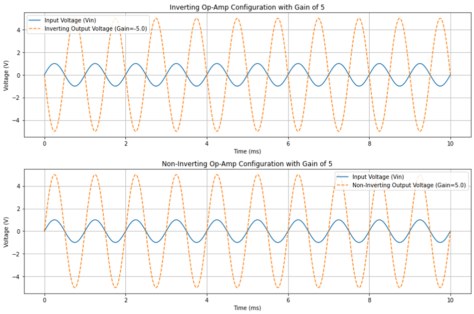
Inverting op-amps apply the input signal to the inverting terminal, resulting in output voltage inversion (180° phase shift). Non-inverting op-amps apply the input to the non-inverting terminal, preserving the signal phase.
The gain of an inverting op-amp is determined by the ratio of feedback to input resistors with a negative sign, while the non-inverting op-amp gain equals one plus the feedback-to-input resistor ratio, always positive and greater than or equal to one.
Inverting op-amps have input impedance defined by the input resistor, which can be controlled, whereas non-inverting op-amps offer very high input impedance, minimizing loading on the source. Both provide low output impedance for driving loads effectively.
Non-inverting configurations typically exhibit a higher common-mode rejection ratio (CMRR) and lower noise due to their feedback configuration compared to inverting op-amps, which may be more susceptible to noise and have a lower CMRR.
Inverting op-amps are preferred for signal inversion, summing amplifiers, and differential amplification applications, while non-inverting op-amps are favored for buffering, voltage followers, and applications requiring phase consistency and high input impedance.
Introduction
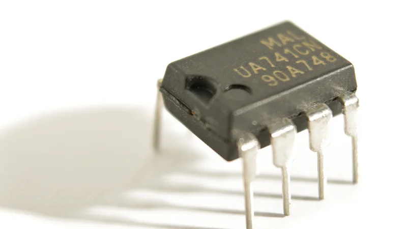
Operational amplifiers (op-amps) are fundamental building blocks in analog electronics, renowned for their high gain and versatility in signal amplification. Featuring two input terminals—one inverting and one non-inverting—and a single output, op-amps amplify the voltage difference between their inputs with remarkable precision. These devices serve critical roles in countless electronics applications, including filtering, oscillation, voltage regulation, and signal conditioning.
The inverting and non-inverting configurations offer distinct operational characteristics that affect gain, phase, input and output impedances, and noise performance.
Inverting op-amps provide output signals with 180-degree phase inversion relative to the input, making them well-suited for applications such as summing amplifiers and signal inversion. Conversely, non-inverting op-amps preserve the input signal phase and offer high input impedance, advantageous for buffer and voltage follower applications.
This article delves into the theoretical underpinnings of both configurations, explores their quantitative performance metrics, common applications, and offers insight into practical design and analysis techniques that optimize their use in modern electronic systems.
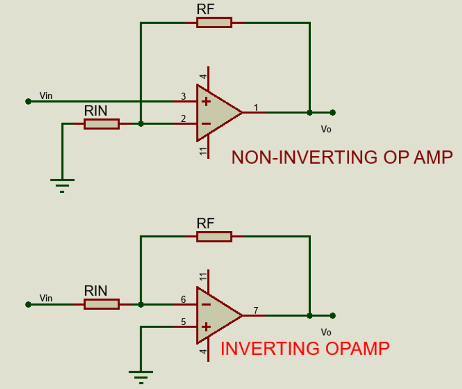
Theoretical Foundations - Inverting vs Non-Inverting Op Amps Modern op-amps achieve closed-loop linearity by applying negative feedback around a high-gain differential core.
In inverting mode, the input drives the “–” node through a resistor network (phase inversion of 180°),
Non-inverting mode drives the “+” node directly (0° phase shift).
Assuming an ideal op-amp with infinite open-loop gain and input impedance, the canonical gains are:

Input-Output Phase Relation
The inverting amplifier takes the input through a resistor into the inverting node, producing an output 180° out of phase with a gain.
The non-inverting amplifier drives the non-inverting node, yielding an in-phase output with the gain. Due to the input-output phase relations, the non-inverting configuration is suited for high input impedance, while the inverting configuration is best for accurate summing/scaling applications.
Noise Gain
Noise gain is the amplification factor applied to the internal noise sources of the op-amp, which appear at the input and are consequently amplified along with the input signal. It differs from the signal gain in how noise components get amplified and directly influences the noise performance and stability of the amplifier circuit.
For both configurations, the noise gain NG is given by:

Even though the signal gain in inverting mode is -Rf/Rin, the noise gain includes the additional 1, representing the contribution of the non-inverting input to overall noise amplification.
For the non-inverting op-amp configuration, the noise gain equals the signal gain since the input signal is applied to the non-inverting terminal.
Design and Analysis Considerations
Below is a repeatable, quantitative approach you can apply in 2025 designs.
Choose Topology from System Needs
Selecting the appropriate operational amplifier (op-amp) configuration depends primarily on the system requirements:
Input Impedance | If a very high input impedance (in the megaohm range) is required, the non-inverting configuration is preferred because it offers extremely high input impedance. The inverting configuration input impedance approximately equals the input resistor, which is generally lower. |
Gain Under Unity | The inverting configuration allows a gain of less than one (attenuation). The non-inverting configuration’s gain has a minimum of 1 V/V, meaning it cannot attenuate signals. |
Multiple Input Processing | The inverting input node simplifies the summation of multiple inputs with precise weights, thanks to its virtual ground characteristic. |
Phase Considerations | If non-inverted polarity is required in output, choose the non-inverting topology. Otherwise, phase inversion by an inverting amplifier can be compensated digitally or by adding another amplifier stage. |
Check Bandwidth from Gain-Bandwidth Product and Loop Gain
For voltage-feedback, unity-gain stable op-amps, the closed-loop bandwidth approximately equals

where GBW is the gain-bandwidth product.
Increasing noise gain results in lower bandwidth.
This is consistent with loop-gain analysis: the 0 dB crossover frequency occurs when

Suggested Reading: Low Pass Filter vs High Pass Filter – Theory, Design, and Applications
3. Verify Slew Rate and Large-Signal Behavior
Ensure the required slew rate exceeds the minimum:
- It is best to provide at least a twofold margin over this minimum to prevent distortion at full-scale output.

4. Noise Budgeting
The output noise voltage density

where ;
en is input voltage noise,
in is input current noise, and
4kTR terms are thermal noise components
The non-inverting amplifier always amplifies the input voltage noise by the noise gain NG
5. Stability at Low Gains
At low closed-loop gains, non-inverting amplifiers can have lower noise gain compared to inverting amplifiers.
Some op-amps are decompensated and not unity-gain stable, requiring a minimum noise gain for stable operation.
Meeting the minimum stable gain is crucial; it is often easier to achieve the required stability margin with inverting configurations by choosing appropriate resistor values to control noise gain.
Common Applications - From Sensing to Signal Conditioning
Precision Sensors (Bridge, RTD, Strain)
Non-inverting op-amps are ideal front ends for precision sensors because they maintain very high input impedance (≥ 1 MΩ), which prevents loading and signal distortion. Their configuration also simplifies managing the common-mode rejection ratio (CMRR), essential for accurately measuring small sensor signals in noisy environments.
Typical designs use gains around 11 with resistor ladders, balancing bandwidth and noise. Pairing them with low-frequency noise op-amps reduces drift below 10 Hz, improving measurement stability and fidelity.
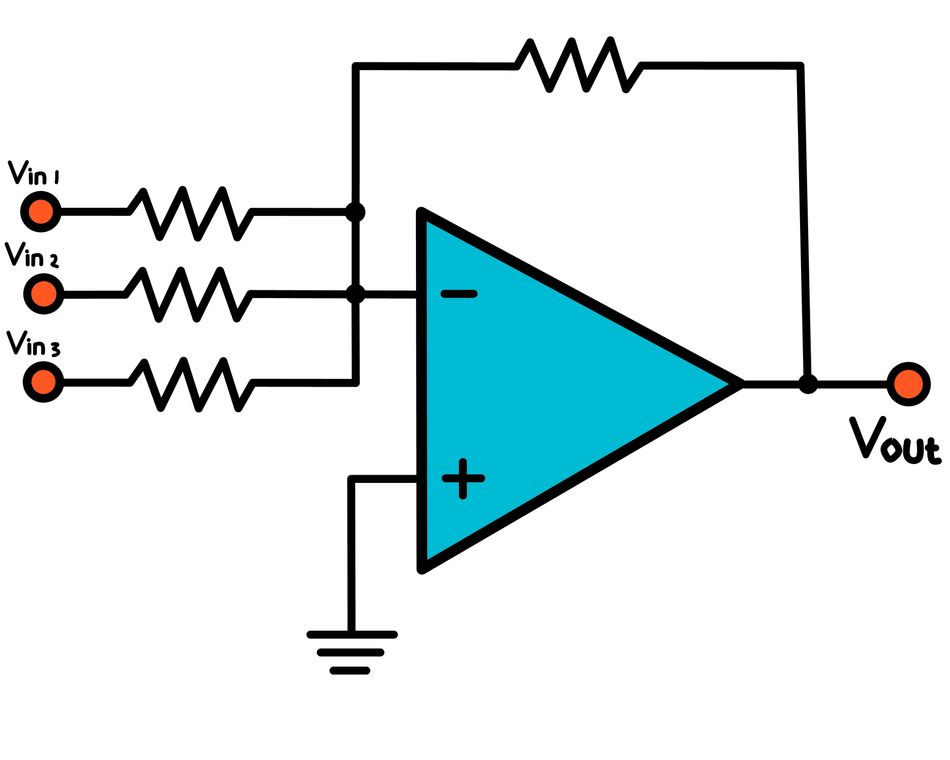
Active Summing for Audio and Data Acquisition (DAQ)
Inverting op-amps excel at summing multiple input signals with precise weighting due to their virtual ground input node. This makes them highly suitable for audio mixers and DAQ systems requiring linear addition of signals.
With precise resistor selection, signal mixing achieves high stability and accuracy, supporting resistor tolerances as tight as ±0.1%, which guarantees predictable and low-distortion summing.
Feature | Benefit |
Summing Capability | Multiple weighted inputs summed |
Resistor Tolerance | ±0.1% yields a predictable mix |
Level Shifting for ADC Range
Non-inverting amplifiers combined with a voltage reference are used to shift bipolar sensor outputs to fit unipolar ADC input ranges. This is crucial when sensor outputs span negative to positive voltages and must be linearly mapped within the ADC’s input limits.
Designs prioritize rail-to-rail input/output op-amps to minimize headroom losses, maximum dynamic range, and measurement accuracy.
Suggested Reading: Accurate Measurements using Shunt Resistors and Current Sense Modules in High-Energy Storage Applications
Unity-Gain Buffers
Non-inverting buffers configured for unity gain provide isolation without gain, preserving signal integrity while preventing source loading. They require unity-gain-stable, high-performance op-amps to handle fast signals with minimal noise.
Characteristics include bandwidths in hundreds of MHz, high slew rates, and ultra-low voltage noise densities, making them well-suited for sensitive sensor outputs.
Integration with ADC drivers and Filters
Driving SAR ADCs
Fully-differential amplifiers (FDAs) are often analyzed like inverting VFAs. Stability depends on noise gain and loop-gain crossover—compensation networks (RC snubbers at the ADC input) shape NG to restore ≥45–60° phase margin.
Anti-alias Filters
Inverting Sallen-Key and multiple-feedback (MFB) topologies exploit the inverting node’s virtual ground for stable, precise Q. Verify stopband noise-gain ≥ 1 to avoid unexpected peaking.
Reference shifting
The non-inverting with reference design centers signals in the ADC window without adding extra stages—reducing noise accumulation and cost.
Suggested Reading: Difference between Active and Passive Filters?
Modern Software Tools Revolutionize Implementation
Simulation software tools have significantly evolved in 2024 and 2025, offering powerful platforms that simplify and optimize analog design, especially for operational amplifier circuits.
LTspice (Analog Devices, 2024) - Recognized for its fast transient simulation and extensive vendor model libraries, LTspice excels in simulating analog circuits quickly and accurately. It includes rich op-amp models with flags indicating minimum stable gain for stability assessments. Designers leverage LTspice to reliably analyze loop gain and phase margin before hardware layout.
TINA-TI / PSpice for TI (Texas Instruments, 2024) - These simulators provide application-note-accurate models, including specialized drivers for analog-to-digital converters (ADC) and noise-gain shaping techniques applicable to fully differential amplifiers (FDAs). This makes them highly useful for mixed-signal system design.
QSPICE (Qorvo, 2024) - Offering SPICE core simulation enhanced by C++-based device modeling flexibility, QSPICE supports custom loop and compensation routines favored in advanced industry use.
Multisim (National Instruments, 2024) - Primarily used in education and rapid prototyping, Multisim integrates graphical measurement tools with vendor-accurate macromodels and robust AC noise analysis, facilitating noise and stability evaluations in a user-friendly interface.
Best Practices Address Common Implementation Pitfalls
To ensure robust and stable designs, several practical guidelines help address frequent challenges in op-amp circuits:
Capacitive Loads & Long Traces - Adding a series output resistor (typically 10–50 Ω) or snubber circuit is effective in controlling peaking caused by capacitive loads and long cable runs. Always validate a phase margin ≥45° to maintain stability.
Input Bias Currents - Minimize input offset by carefully matching impedance at both inputs, particularly critical for bipolar input stages. Maintain DC balance by mirroring feedback and gain resistors seen by the non-inverting input.
Resistor Values - Avoid excessively high feedback resistor values (>100 kΩ) on high-speed voltage feedback amplifiers (VFAs), as thermal noise (4kTR and input bias current offsets becomes significant. Typical resistor selections are within 1–10 kΩ for balanced noise and offset performance.
Suggested Reading: Resistor Chart: Comprehensive Guide to Resistor Values, E-Series, and Color Codes
Minimum Stable Gain - Decompensated op-amps require noise gain (NG) to meet or exceed a minimum stable value to avoid oscillations. Unity-gain stable devices are recommended for buffer stages.
Layout & Grounding - Critical nodes, especially the inverting input, should be kept physically compact and treated as “virtual grounds.” Analog and digital grounds should be separated, loop areas minimized, and sensitive nodes shielded, following manufacturer guidelines from TI and ADI.
Advanced Techniques Reveal Sophisticated Applications
Emerging approaches provide design flexibility with optimal performance:
Gain-Range Agility with Fixed Noise Gain
Precision systems maintain a constant noise gain for stable bandwidth and phase margin, varying signal gain by switching input resistor banks in inverting configurations. This approach keeps bandwidth effectively constant while adjusting gain.
Noise-Optimized Attenuators (Gain < 1)
Even with attenuation, noise gain remains ≥1. Employ low-noise input voltage amplified op-amps and minimize resistor values to reduce Johnson noise. Chopper or auto-zero amplifiers can be beneficial in suppressing 1/f drift—an important factor in low-frequency precision measurement.
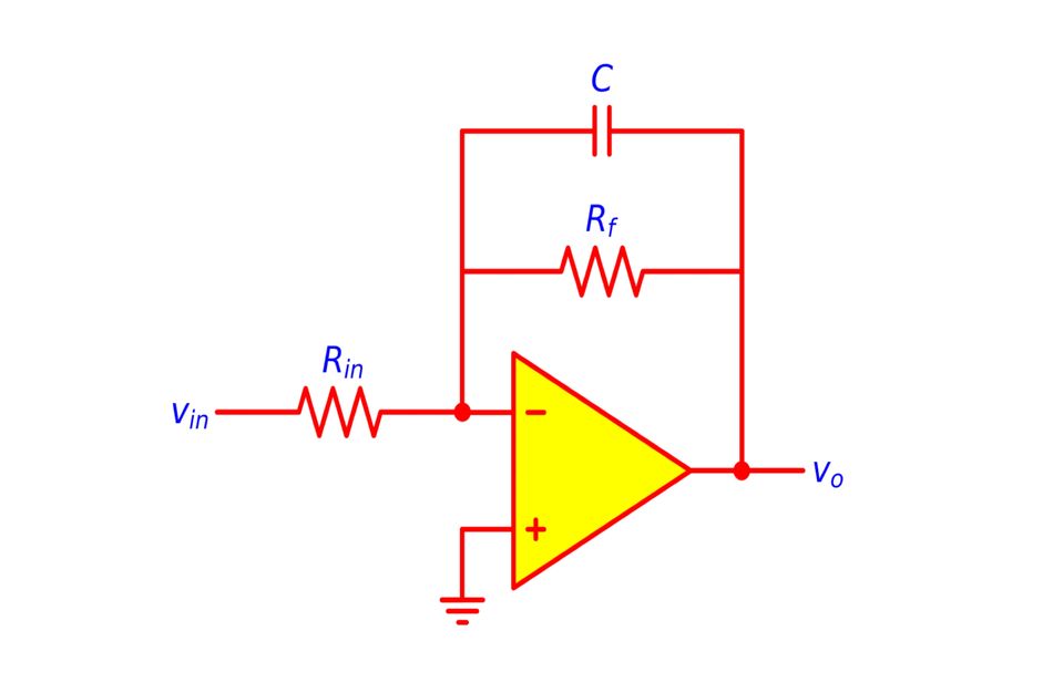
Compensating Capacitors Across Feedback Resistors
Adding small capacitors across feedback resistors helps shape noise gain frequency response, rolling off high-frequency gain and enhancing stability margins. Simulation validation via AC and transient analysis ensures passband flatness and required stability.
Design Examples for Inverting and Non-Inverting Amplifiers
Example 1 — Non-Inverting Sensor Amplifier (Gain = 11 V/V)
The non-inverting amplifier circuit takes the input signal from a sensor and outputs an amplified signal without inverting its polarity. This configuration is preferred when preserving the original phase and ensuring a very high input impedance to avoid loading the sensor signal source. It uses a feedback resistor and a gain resistor arranged to set the closed-loop gain.
Design and Parameters:
The target is to amplify a 100 mV peak sensor signal to approximately 1.1 V peak output, corresponding to a gain of 11. An op-amp with a gain-bandwidth product (GBW) of about 50 MHz and unity-gain stability is chosen to ensure sufficient bandwidth and stable operation.
The resistors selected are:
Gain resistor Rg=1 kΩ
Feedback resistor Rf=10 kΩ
These set the gain to 11, because noise gain equals the signal gain in this configuration, the estimated closed-loop bandwidth is roughly
50 MHz / 11 ≈ 4.5 MHz
The slew rate requirement for a maximum 100 kHz signal is calculated as approximately 0.69 V/µs, so the chosen op-amp should exceed 2 V/µs to provide adequate margin against distortion at full-scale.
Example 2 — Inverting Audio Mixer Stage
The inverting amplifier configuration is used here to sum multiple audio source signals with precise weighting. Each input signal passes through its own input resistor into the summing node (virtual ground) of the op-amp, allowing linear addition of weighted inputs. The inverted output contains the sum of these signals multiplied by their respective gains.
Design and Parameters:
The aim is to mix two audio inputs, each amplified with an individual gain of –2.
Resistor values chosen are:
Feedback resistor Rf=20 kΩ
Input resistors Rin1=Rin2=10 kΩ
These define each input gain as −Rf/ Rin=−2
Noise gain for each path is 3, resulting in an estimated bandwidth around 10 MHz if the op-amp has a GBW of 30 MHz.
An additional 22 Ω output resistor is included to stabilize loads such as cables or capacitive elements typically found in audio environments.
Recommended Reading: The Audio Revolution at the Edge
Conclusion
Understanding the differences and appropriate applications of inverting and non-inverting operational amplifier configurations is vital for designing effective analog circuits. The inverting configuration, characterized by its phase inversion, precise linear summing capability, and controllable input impedance, is ideal for applications such as audio mixers, signal processing, and weighted summation tasks. Despite introducing a 180-degree phase shift, it offers flexibility in gain adjustments and simple input impedance control through resistors. Conversely, the non-inverting configuration provides high input impedance and preserves signal phase, making it preferable for buffering sensor outputs, level shifting to interface with ADCs, and applications where signal integrity and minimal loading are crucial.
Modern design frameworks integrate detailed gain and noise gain calculations, bandwidth and slew rate considerations, and robust stability analysis. Coupled with advanced software simulation tools and best layout practices, designers can optimize amplifier circuits to meet demanding precision, speed, and noise requirements. Ultimately, the choice between inverting and non-inverting amplifiers hinges on system needs such as input impedance, gain range, phase constraints, and noise performance, enabling tailored solutions across diverse electronics applications.
FAQs
Which op-amp is better to use in 2025: inverting or non-inverting?
There is no one-size-fits-all answer. The choice depends on what your circuit needs. Use a non-inverting op-amp when you want very high input impedance or need to buffer signals without loading the source. Choose an inverting op-amp when you want to sum multiple signals accurately or need gains less than one (attenuation). Regardless of topology, always design with noise gain and phase margin in mind for stability and best performance.
Why does the gain formula for non-inverting op-amps always include a “plus one”?
This happens because part of the output voltage is fed back into the amplifier’s inverting input to balance the inputs. This feedback creates a minimum gain of one, meaning the output is at least as big as the input, even without any additional gain from the resistors.
Can an inverting op-amp have gain less than one?
Yes, by choosing appropriate resistor values, an inverting amplifier can reduce the signal size (attenuate it). On the other hand, non-inverting op-amps cannot have gains less than one; their minimum gain is unity.
Which configuration is quieter?
It depends on your specific setup. Both amplify the internal voltage noise by their noise gain. Inverting amplifiers also add some noise from the input current flowing through resistors. To minimize noise, choose resistor values and op-amps carefully based on your desired frequency range.
Why does my buffer circuit oscillate when set to unity gain?
Your op-amp might not be stable at unity gain if it’s not designed for it, or if the load (like a cable or capacitor) causes instability. To fix this, either use an op-amp that is unity-gain stable or add a small resistor or snubber circuit at the output, and ensure the stability margin (phase margin) is sufficient.
Does a non-inverting configuration have higher bandwidth than an inverting one?
For the same noise gain, their bandwidths are similar. In practice, non-inverting circuits often show slightly higher bandwidth at the same signal gain, but this should be verified for each design by analyzing the loop gain.
References
Cadence Design Systems, "Inverting vs Non-Inverting Op-Amp: A Comparison," Cadence PCB Resources. [Online]. Available: https://resources.pcb.cadence.com/blog/2024-inverting-vs-non-inverting-op-amp-a-comparison
Texas Instruments, "Using noise-gain shaping to stabilize fully-differential amplifiers," Application Report SLYT733. [Online]. Available: https://www.ti.com/lit/pdf/slyt733
Texas Instruments, "Op Amp Noise and Noise Gain," Application Report SBOA263. [Online]. Available: https://www.ti.com/lit/pdf/sboa263
Analog Devices, "Op Amp Issues: Noise Gain," Analog Dialogue. [Online]. Available: https://www.analog.com/en/resources/analog-dialogue/articles/op-amp-issues-noise-gain.html
All About Circuits, "Understanding Operational Amplifier Slew Rate," AllAboutCircuits.com. [Online]. Available: https://www.allaboutcircuits.com/technical-articles/understanding-operational-amplifier-slew-rate/
Texas Instruments, "Undistorted Slew Rate Measurements on Operational Amplifiers," Application Report SLOA011. [Online]. Available: https://www.ti.com/lit/pdf/sloa011
Toshiba Semiconductor, Toshiba Semiconductor Storage Site. [Online]. Available: http://toshiba-semicon-storage.com/
Analog Devices, "FAQ: Op Amp Applications," Analog Dialogue RAQ Issue 91. [Online]. Available: https://www.analog.com/en/resources/analog-dialogue/raqs/raq-issue-91.html
Texas Instruments, "Op Amp Gain Bandwidth Product," Application Note SBOA092B. [Online]. Available: https://www.ti.com/lit/an/sboa092b/sboa092b.pdf
Electronics Tutorials, "Op-Amp Tutorial 3," Electronics-Tutorials.ws. [Online]. Available: https://www.electronics-tutorials.ws/opamp/opamp_3.html
Electronics Tutorials, "Op-Amp Tutorial 2," Electronics-Tutorials.ws. [Online]. Available: https://www.electronics-tutorials.ws/opamp/opamp_2.html
Wikipedia, "Operational Amplifier Applications," Wikipedia.org. [Online]. Available: https://en.wikipedia.org/wiki/Operational_amplifier_applications
Electrical Engineering Stack Exchange, "Bandwidth of inverting and non-inverting op-amps," Electronics Stack Exchange. [Online]. Available: https://electronics.stackexchange.com/questions/200665/bandwidth-of-inverting-and-non-inverting-op-amps
in this article
1. Key Takeaways2. Introduction3. Design and Analysis Considerations 4. Common Applications - From Sensing to Signal Conditioning5. Integration with ADC drivers and Filters 6. Modern Software Tools Revolutionize Implementation7. Best Practices Address Common Implementation Pitfalls8. Advanced Techniques Reveal Sophisticated Applications9. Design Examples for Inverting and Non-Inverting Amplifiers10. Conclusion11. References