Are GaN semiconductor power components ready for automotive?
Offering high power performance and high-frequency switching, GaN semiconductors present huge potential.

Last updated on 29 Jun, 2020. 7 minutes read
What is GaN Technology?
Gallium Nitride (GaN) is a material with high heat capacity and thermal conductivity used in the production of semiconductor power devices such as GaN FET (field-effect transistor).
GaN semiconductors are poised to replace silicon as the semiconductor of choice for high voltage power devices as they can operate at higher frequencies, with increased efficiency and higher power density - providing the basis to create smaller, more efficient, and more robust power devices.
These attributes are largely thanks to GaN’s wide band gap. Band gap is an energy range between a semiconductor’s valence band and conduction band where electron states are forbidden. A wide band gap allows devices to operate at much higher voltages, frequencies, and temperatures than conventional semiconductors. GaN has a band gap of 3.2 eV, in comparison, silicon has a bandgap of just 1.1 eV.
GaN is successfully applied in RF (Radio Frequency) components, and light-emitting diodes (LEDs). The blue light in your old BluRay player is created using a GaN-based violet laser diode. It’s also present in solar cells for photovoltaic systems and is an essential component of energy-efficient LED globes. GaN is used in radiation-hardened transistors for satellites and is quickly replacing silicon in this area due to its small physical die size. GaN microwave transistors will be onboard The Earth Explorer Biomass satellite set to launch 2021 which will provide global maps of the amount of carbon stored in the world's forests. GaN is also showing up in consumer power devices such as lightning-fast mobile and laptop chargers.
The automotive industry is the next challenge for GaN to tackle. Although proven to outperform reliable silicon, the question remains if GaN can deliver the quality, reliability, and scalability in manufacturing required by the demanding automotive market.
But Wait, What’s Wrong With Silicon?
It is widely accepted that silicon is reaching its physical limit. While continuing to be a highly reliable semiconductor material in many applications, silicon is limited when it comes to high-frequency switching and power density. Some incremental improvements in silicon increase some parameters but these improvements generally result in a loss in other parameters. This means new silicon uses will become more application-specific where these losses have less of an impact. Even with incremental gains, it is clear, there is a near-future limit on power density and frequency available from silicon.
The limitations of silicon in high-frequency and high power applications were seen early by the industry and investigations into other materials have been progressing in the background for decades. One of the leading contenders is GaN - outperforming silicon for higher voltage applications in most comparisons even when it's in early maturity stages.
GaN’s significantly wider bandgap means current can travel faster through GaN semiconductors, ensuring greater efficiency and fewer switching losses when they are used in hard switching applications. They also lose less power when devices are charged and discharged thanks to having less capacitance than silicon metal-oxide semiconductor field-effect transistors (MOSFETs). Finally, they also take up much less space on circuit boards pushing open the opportunity for smaller and smaller appliances.
Silicon most likely will continue to remain king in lower power and lower frequency devices as well as processing applications but with the electrification of rapidly advancing industries such as automotive, space, and the military more robust alternatives such as Gallium Nitride are required.
GaN: the good, the bad, and the better
GaN was first explored in the 1990s but its maturation has been slow due to some key challenges. Developing a reliable and consistent manufacturing process for GaN has been difficult in comparison to the reliability of silicon.
Gallium Nitride contains a massive number of crystal defects over a small area compared to silicon which contains as low as 100 defects per square centimeter. Only very recently have researchers been able to manufacture GaN effectively with fewer than one billion defects/cm. This problem has been largely overcome but the cost to produce the same amount of GaN wafers compared to silicon is still notably higher.
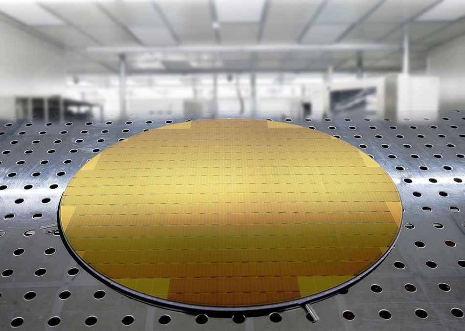
A successful strategy for GaN development while maintaining the large-production ability of silicon is GaN-on-Si. Thick GaN epitaxial layers are grown on large silicon substrates in standard 150 mm (6 inch) fabs. GaN-on-Si offers true scalability with manufacturing confidence.
GaN in the Automotive Industry
The automotive industry is quickly electrifying with a global number of electric passenger cars passing 5 million in 2018, an increase of 63% from the previous year. Positive forecasts suggest electric vehicle (EV) sales will reach 44 million vehicles per year by 2030.
For this growth to continue, electric cars are being pushed to be both more efficient and lower cost.
Despite headway being made towards more efficient, lighter, and smaller batteries - this core feature of EVs remains the number one obstacle to overcome before the introduction of the next generation of cheaper and more efficient vehicles.
While battery development grinds away, innovation is driving major powertrain improvements. Efficiency increases in each component of an EV powertrain can have a significant impact on the overall efficiency of the vehicle through a reduction in weight and overall smaller physical size allowing for alternative design layouts.
GaN Powertrain Components
GaN delivers on smaller, more efficient, and lower-cost power systems thanks to its ability to offer lower switching loss, faster-switching speeds, increased power density, and improved thermal budgets. The power density and efficiency of GaN will have the biggest impact in three areas of electric vehicle and hybrid vehicle design.
Onboard Charger
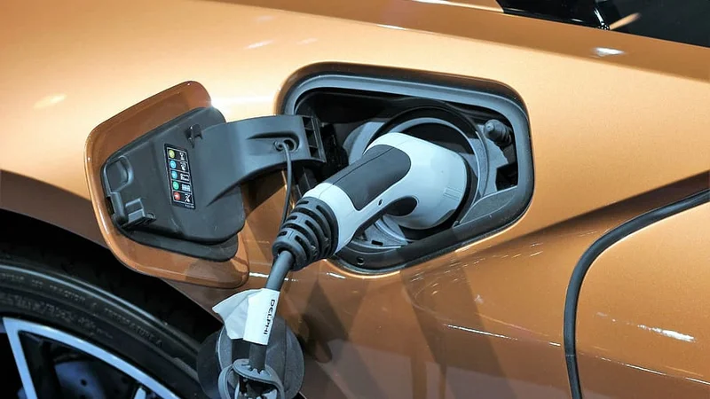
An on-board charger (OBC) in an EV or hybrid electric vehicle (HEV) is used to charge the traction battery. The On-Board charger system converts the AC power from the grid to a DC input which charges the battery. Using GaN semiconductors can result in OBC’s that are lighter and smaller than their current physical size. This decrease in size and weight indirectly provides the vehicle with a longer driving range via an overall decrease in vehicle weight.
Improved OBC efficiency will also reduce car charging times. Currently, a full charge at a 50 kW charging station takes about 50 minutes and gives a driving range of about 200 Km (125 miles). Fine for commuters, but a huge deterrent for people looking to make longer trips. The goal for the industry is to reach 35 kW charging stations that would drop the charging time down to less than ten minutes, the perfect restroom or coffee break time - and a comparable time to what we now experience stopping for petrol for a combustion engine vehicle.DC-DC Converter
DC-DC converter bridges the high-voltage battery pack with the vehicle’s low voltage auxiliary circuits. The use of GaN semiconductors in DC-DC converters result in devices that are highly efficient, reducing loss and wasted power to heat, and featuring best in class power density. This one efficient design change contributes significantly to the overall weight decrease of the car resulting in better range.Traction Inverter
Within an electric vehicle’s drivetrain, the traction inverter converts DC current from the battery to AC current used by the motor to power the vehicle’s propulsion system. The most common three-phase AC motors used in today’s EVs run at voltages up to 1,000 V and switching frequencies up to 20 kHz. This configuration bumps close to the current operational limits of the silicon-based MOSFETs and insulated-gate bipolar transistors (IGBTs) currently used in traction inverters.
GaN technology pushes past these limits. A highly efficient traction inverter with GaN components provides longer range, fewer charging cycles, and extended battery life with similar battery costs. Operating at 30 kHz it provides the opportunity to use smaller, more efficient, and powerful electric motors and consequently smaller, cheaper, and lighter batteries to achieve the same driving range. These improvements would help enable manufacturers to get closer to price parity with internal combustion engine vehicles and thus extending the market reach of Evs

Conclusion
GaN semiconductor power devices will usher in a new era of electric vehicle powertrain components that will deliver more efficient vehicles. Innovative collaborations between semiconductor manufacturers and automotive companies will drive innovation and speed up the technology adoption. The full potential of GaN semiconductor power components is likely to be fully realized within the next decade, paving the way to a greener and more efficient future.
About the sponsor: Nexperia
Power GaN FET solutions
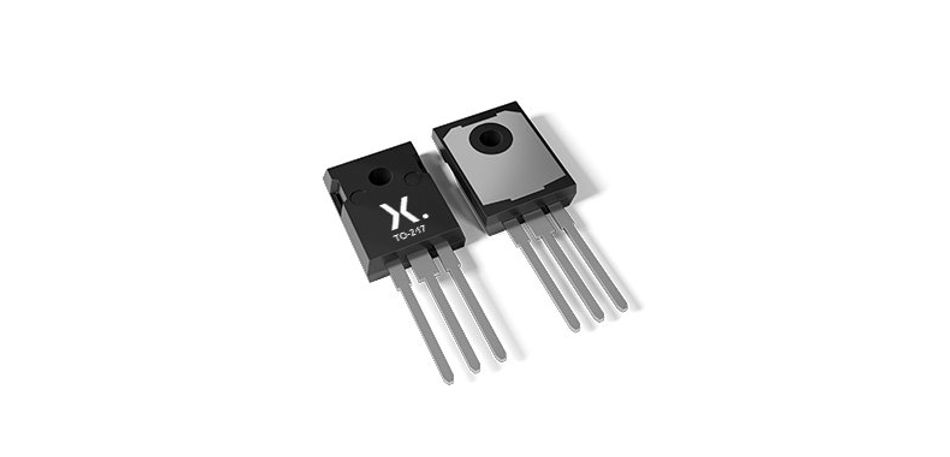
Semiconductor manufacturer Nexperia is tackling the manufacturing issues of GaN by developing processes that utilize existing Si-based technology and infrastructure ready for large volume mass production. While the technology is still in early maturity stages it has proven its robustness for commercial application and the best is yet to come. Nexperia Power GaN products such as the GAN063-650WSA are primed for use in the automotive industry and already perform to AEC-Q101 standard qualification standards.
Research and development show promising results for GaN’s success in EV traction inverters. To close the gap between the lab and an applied tested product, Nexperia, has teamed up with Ricardo, an automotive engineering consulting company, to put its GaN devices into a 50 kW EV traction inverter for extensive testing. The collaboration is rigorously testing the GaN components to look for any possible weaknesses or failure points in an applied EV setting.
The project also works to demonstrate to the wider automotive industry the huge potential of GaN. The results of the project, which we expect to see later in 2020 and early 2021 will be of interest to a lot of automotive designers and provide real value to the industry as a whole.
Curious about GaN and its applications in the automotive industry?
2-3 July 2020, Nexperia is hosting an online event called 'Power Live' to share knowledge about their work on power semiconductors. One of the event's 4 tracks is completely dedicated to GaN, and the 'automotive' and 'packages' tracks also cover GaN.
Engineers of Nexperia and their partner Ricardo will share share their insights: From tackling common application issues with GaN FETs to a deep dive into the development of their GaN based traction inverter.
You can read more and register for Nexperia’s Power Live Event here.