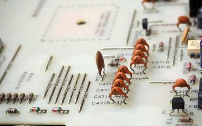
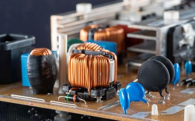
Capacitors in parallel are ubiquitous in digital and analog hardware. When used properly, they increase capacitance, reduce unwanted impedance and noise, and improve power integrity across a broad frequency range.
Be the first to know.
Get our pcb weekly email digest.
Tagged with
PCB
ORGANIZATIONS. SHAPING THE INDUSTRY.


HQ NextPCB
Appliances, Electrical, and Electronics Manufacturing
HQ NextPCB specializes in reliable multilayer PCB manufacture and assembly ...
1 Post

AllSpice
Software Development
Hardware collaboration platform 🤖 Inspired by software development princip...

Latest Posts
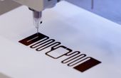
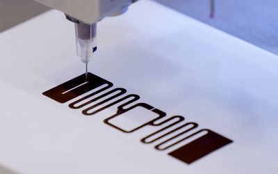
Trying to keep up with the ever-shrinking requirements of consumer electronics? Looking to cut every milligram of fuel-wasting weight in automotive and aerospace? The design options printed electronics offer go far beyond what can be achieved with the rigid PCBs of the past.
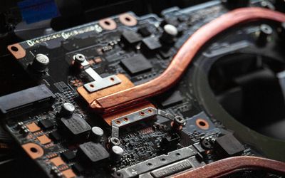
This blog post dives deep into the essentials of thermal management in PCB design, covering key techniques like PCB thermal vias design, PCB heatsink selection, thermal simulation for PCBs, PCB material thermal conductivity, and high power PCB thermal design.
Enhancement-mode and depletion-mode MOSFETs are types of field-effect transistors with opposite default states—normally off vs. normally on. This guide breaks down their behavior, biases, equations, real-world uses, and 2025 tech trends.

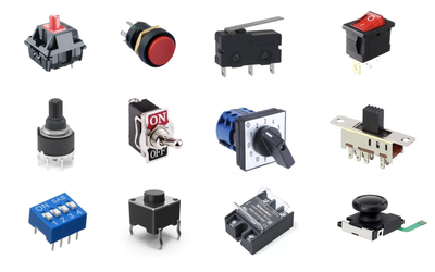
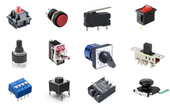
This technical guide details various types of switches, highlighting their configurations, functionality, emerging technologies, and selection criteria for choosing a right one for your application!
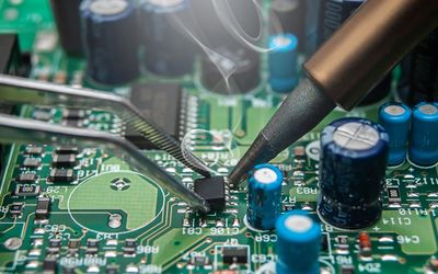
Desoldering is the process of removing solder to detach components from a PCB. Whether you're repairing hardware, modifying a design, or salvaging parts, this hands-on guide walks you through the tools, techniques, and safety tips every electronics pro needs.
PCB etching is a chemical process that removes copper to form circuits. This guide covers fast etchants, FeCl₃ reactions, AI-driven optimization, aerospace standards, and sustainable methods for high-density PCBs in 5G and medical applications.
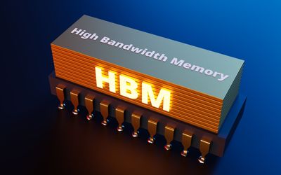
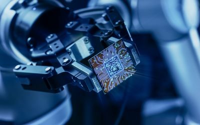
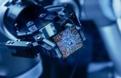
What is High Bandwidth Memory 3 (HBM3)? This comprehensive engineering guide covers architecture, applications, and performance, along with some advanced techniques used by leading AI companies and best implementation strategies!

event | OCT 31 - NOV 02, 2025

Hackaday Supercon is returning for an exciting weekend filled with technical talks, badge hacking, and hands-on workshops

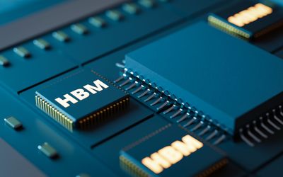
Master HBM memory technology with our comprehensive engineering guide covering 3D stacking architecture, bandwidth calculations, and design optimization techniques. Discover implementation strategies for AI and HPC applications!
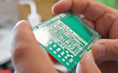
This technical guide explores the various types, material properties, manufacturing processes, and key design considerations associated with blank PCB technology!

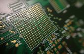
Ball Grid Array (BGA) is a high-density packaging technology using solder balls for connections. This guide covers BGA design principles, performance advantages, modern applications (2000+ pins in 45mm), and cutting-edge implementation techniques for engineers.

This article presents rigid-flex circuit board design guidelines for the development of a core body temperature (CBT) sensor device.

OEM means the client designs and the manufacturer builds. ODM means the manufacturer handles both design and production. This guide helps engineers compare IP control, customization, cost, and time to market to decide which model fits their product best.
Watch the webinar on sustainable PCB manufacturing hosted by Voltera and Jiva Materials.