PCB Etching: Complete Process Guide & Best Practices
PCB etching is a chemical process that removes copper to form circuits. This guide covers fast etchants, FeCl₃ reactions, AI-driven optimization, aerospace standards, and sustainable methods for high-density PCBs in 5G and medical applications.

01 Jul, 2025. 15 minutes read
Introduction to PCB Etching
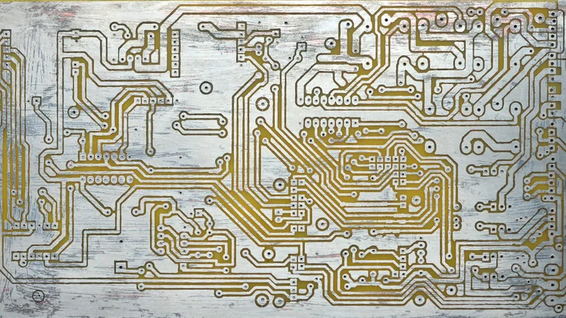
PCB etching is a critical step in the PCB manufacturing process, transforming a plain copper board into a functional printed circuit board by chemically removing unwanted copper to define precise copper traces. This selective material removal relies on the use of specialized etchants like ferric chloride, cupric chloride, or hydrogen peroxide blends to dissolve exposed copper areas, while protected regions remain intact, thanks to materials like photoresist, toner, or etch resist.
As the demand for high-density interconnects grows in fields like 5G, medical electronics, and automotive systems, mastering the etching process is more important than ever. Modern techniques can achieve etch rates of over 10 µm/min and feature resolutions under 25 µm, enabling the fabrication of complex PCB designs with ultra-fine vias, through holes, and multilayer structures on various laminates.
Engineers and designers must understand both the fundamentals and cutting-edge aspects of PCB etching. This includes mastering core chemical reactions and masking techniques, while also exploring innovations like AI-optimized etching parameters and sustainable process alternatives. As the industry evolves, integration with digital twin technologies is reshaping how prototypes are tested and refined, enabling smarter, faster design cycles. Whether you're a DIY hobbyist using a laser printer for toner transfer or a professional aiming for aerospace-grade tolerances, adapting to these trends is essential.
Theoretical Foundations Reveal PCB Etching's Chemical Precision
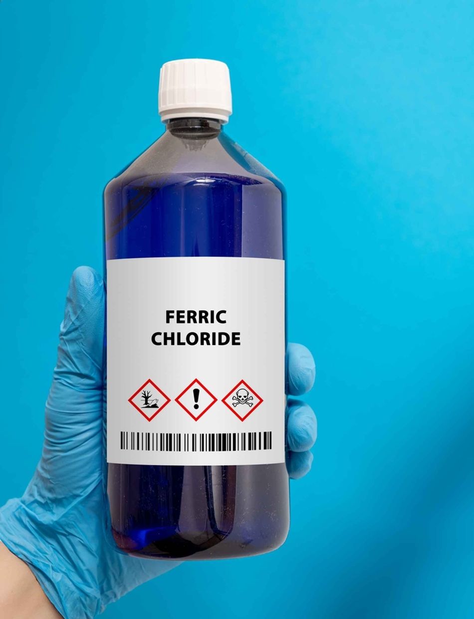
At the heart of the PCB etching process lies a controlled chemical reaction designed to selectively dissolve copper from a printed circuit board. The most commonly used etchant in both industrial and DIY applications is ferric chloride, which reacts with metallic copper to produce soluble copper chloride:
Cu + 2FeCl₃ → CuCl₂ + 2FeCl₂
This reaction showcases why ferric chloride remains a popular choice—it offers a high copper removal efficiency of up to 99.8% when properly maintained. Alternatives like cupric chloride or hydrogen peroxide/hydrochloric acid mixtures are also used in modern PCB manufacturing, especially where tighter control of the etch rate and waste management is required.
Selectivity in the etching process is achieved by applying a photoresist, toner, or etch resist pattern on the copper board, protecting the intended copper traces and exposing only the unwanted areas to the etchant. This masking ensures dimensional accuracy, which is critical in advanced PCB design, particularly in double-sided, high-frequency, or prototyping applications with sub-100 µm features.
Temperature plays a significant role in reaction kinetics. As governed by the Arrhenius equation, a 10°C increase can double the etch rate, making thermal control crucial in both manual and automated setups. Most industrial systems maintain temperatures between 45–55°C to balance speed with precision.
Understanding the oxidation-reduction dynamics in chemical etching not only helps in choosing the right etching solution but also informs best practices in substrate preparation, agitation using an agitator, and even etchant regeneration, especially important for sustainable, high-quality production.
Recommended reading: Blank PCB Technology: Technical Guide for Engineers and Designers
Process Techniques Leverage Advanced Chemical Control
Modern PCB etching is no longer a trial-and-error craft—it’s a tightly regulated etching process that leverages both chemical precision and digital oversight to ensure reliable, high-quality results in PCB manufacturing.
The typical sequence for transforming a copper board into a printed circuit board includes five core stages:
Surface Preparation
Before introducing any etchant, it’s essential to clean the laminate surface thoroughly. This removes oxidation, oils, and other contaminants that might interfere with uniform etching. Plasma treatment or a simple abrasive scrub ensures the copper layer on the substrate is fully exposed and ready for patterning.Photoresist or Toner Application
Next, a protective photoresist or toner layer is applied to define the desired copper traces. This etch resist shields certain areas during chemical exposure. Whether you're using a dry film resist, UV-curable photoresist, or a toner transfer method from a laser printer, this step is crucial for pattern fidelity, especially when working on double-sided or through-hole boards.Etchant Exposure
In this critical phase, exposed copper areas are dissolved by the chosen etchant, such as ferric chloride, cupric chloride, or a mix of hydrochloric acid and hydrogen peroxide. The etch rate depends on several factors, including temperature, etching solution concentration, and agitation. Using an agitator ensures turbulent flow over the copper surface, minimizing undercuts and promoting uniform material removal across the entire PCB board.Resist Stripping
Once etching is complete, the remaining etch resist is stripped away, revealing the final copper traces. At this stage, even slight resistance to adhesion issues can cause defects or misaligned vias, so careful removal using acetone or alkaline solutions is recommended.Final Inspection and Cleaning
The etched PCB is cleaned, inspected for defects, and prepped for additional processes like solder mask application, drill hole creation using a drill press or CNC, and optional tin plating to prevent further oxidation.
Recommended reading: PCB Manufacturing Process: A Comprehensive Guide to Understanding and Mastering the Techniques
By mastering each step and monitoring key parameters, especially etchant concentration and etch rate, manufacturers and DIY engineers alike can produce high-quality prototyping boards or production-ready layouts with precision and repeatability.
Common Applications Span from Consumer Electronics to Aerospace
The versatility of the PCB etching process makes it indispensable across a wide spectrum of industries. By selectively removing copper from the substrate, manufacturers create tailored printed circuit boards that power everything from wearable devices to spacecraft systems.
Here’s a closer look at how different sectors apply PCB manufacturing and why etching precision matters:
1. Consumer Electronics
Smartphones, tablets, laptops, and IoT devices are built on densely packed PCB boards. These products demand high-quality etching to achieve miniaturized copper traces and vias, ensuring signal integrity in compact spaces. With billions of square feet of laminate processed annually, the consumer market drives demand for cost-efficient, rapid-turnaround etching solutions.
2. Automotive Electronics
Modern vehicles contain up to 200 electronic control units (ECUs), each powered by printed circuit boards that must endure vibration, heat, and extreme climate shifts. Automotive-grade PCB etching maintains dimensional tolerances within ±10 µm, ensuring the reliability of safety-critical systems like ABS and airbags.
3. Telecommunications Infrastructure
5G base stations, fiber-optic routers, and satellite transceivers require PCB layouts with ultra-fine copper traces and low-loss materials. Here, etchants must work with exceptional selectivity to support trace widths below 25 µm while preserving surface integrity on large-format PCB boards.
4. Medical Devices
From portable diagnostics to implantable monitors, medical electronics rely on PCB fabrication methods that meet stringent standards like IPC-6012 Class 3. The etching process must be exceptionally clean and controlled to ensure biocompatibility and zero-defect yields.
5. Aerospace & Defense Systems
In satellites, avionics, and military gear, PCB manufacturing demands the utmost accuracy and durability. Etchant performance is critical for ensuring consistent copper thickness and trace geometry, factors that affect performance in radiation, pressure, and thermal extremes. These mission-critical applications often use specialized etching solutions and multilayer substrates designed for resilience.
Across these industries, advancements in chemical etching, automation, and AI-driven control are redefining what’s possible in PCB design and manufacturing. Whether for diy hobby projects or space-grade electronics, the same core principles of etchant control and etch rate optimization apply.
Integration with Automation Technologies Enables Smart Manufacturing
The evolution of PCB manufacturing is increasingly defined by smart automation, where intelligent systems optimize every stage of the etching process, from resist application to final inspection. In this new era, integrating advanced control systems with real-time data analytics has redefined how engineers approach both prototyping and mass production.
1. IoT-Enabled Equipment and Etchant Monitoring
Modern etching machines now feature integrated IoT sensors that continuously track parameters such as etchant concentration, temperature, and flow rate. These sensors provide real-time insight into etch rate performance, reducing the margin for error in large-panel PCB production.
2. Machine Learning and Predictive Control
AI-driven software analyzes historical process data to predict and adjust variables like agitation speed and chemical replenishment. This enables optimal removal of copper from the substrate, minimizes undercuts, and ensures consistent results in high-quality PCB boards, especially when using aggressive etchants like ferric chloride or cupric chloride.
3. Digital Twin Technology
Virtual models of the PCB etching process—known as digital twins—allow engineers to simulate chemical reactions, equipment performance, and material behavior before production begins. This innovation is beneficial for refining complex PCB design layouts or experimenting with new etching solution chemistries during diy or research-level prototyping.
4. Automated Pick-and-Place & Inspection Systems
After etching, robotic handling systems move the PCB boards through rinsing, drying, and optical inspection phases. High-resolution vision systems detect trace-level defects, ensuring that vias, copper traces, and drill holes meet design tolerances with micron-level accuracy.
5. Closed-Loop Feedback for Etchant Regeneration
Advanced lines now include automated etchant regeneration units. These maintain optimal chemical activity, especially for hydrochloric acid or hydrogen peroxide blends, ensuring steady etch rates while minimizing chemical waste and environmental impact.
Embracing these technologies allows manufacturers to streamline operations while unlocking greater consistency, sustainability, and scalability in PCB fabrication. Whether you're producing single-sided boards or developing complex double-sided RF systems, automation now drives the excellence at the core of modern PCB etching.
Modern Software Tools Revolutionize PCB Etching Implementation
As PCB design becomes more complex and miniaturized, modern software tools have evolved to address the unique challenges of the etching process. Today’s platforms not only help engineers draft circuit layouts—they also simulate etch rate, predict etchant behavior, and ensure substrate compatibility before a single drop of chemical touches copper.
1. Etching-Aware PCB Design Software
Top-tier programs, such as Altium Designer, OrCAD X, and KiCad, now feature PCB etching simulation modules. These help designers factor in etchant undercut behavior, photoresist shrinkage, and copper trace compensation. Built-in etch resist profiles ensure your design translates accurately from screen to copper board, especially for high-quality applications in medical and aerospace electronics.
2. Etch Rate Optimization and DFM Analysis
Software-integrated Design for Manufacturability (DFM) tools now consider chemical behavior directly within the PCB layout process. By simulating the interaction of ferric chloride, cupric chloride, or hydrogen peroxide mixtures with the laminate, designers can fine-tune line widths, vias, and spacing, resulting in cleaner prototyping with fewer costly revisions.
3. Digital Libraries and Etchant Profiles
CAD platforms often include libraries of etching solution types and process presets. Whether you're working with a toner transfer approach using a laser printer or preparing a multilayer PCB board with fine features, these libraries help you match your etchant and substrate to the desired resolution and tolerance.
4. AI-Powered Design Suggestions
Some tools go a step further by using AI to suggest layout adjustments that improve etching outcomes, such as widening traces in high-density zones or altering drill hole locations to reduce undercuts and thermal stress.
5. Seamless Integration with Fabrication Workflows
Modern platforms output Gerber files, drill files, and chemical process instructions that sync directly with CAM software in PCB manufacturing facilities. This reduces design-to-production turnaround time and enhances yield, especially in double-sided, through-hole, or complex RF board applications.
The combination of intelligent PCB design tools and real-world chemical modeling marks a turning point in PCB etching. From diy hobby projects to industrial fabrication, software is now an essential ally in producing cleaner, more reliable, and cost-effective circuit boards.
Recommended reading: PCB Design: A Comprehensive Guide to Printed Circuit Board Design - Part 1
Best Practices Address Common Implementation Pitfalls
The precision of the PCB etching process depends not only on chemistry but also on rigorous process control. Whether you’re doing diy prototyping or overseeing industrial PCB manufacturing, avoiding critical mistakes ensures high-quality outcomes and longer-lasting printed circuit boards.
Here are five of the most common pitfalls—and how to prevent them:
1. Poor Etchant Management
Overused or saturated etchants, such as ferric chloride or cupric chloride, lose effectiveness and create uneven copper removal. In professional settings, real-time monitoring of etching solution concentration and copper loading is vital. DIY users should avoid letting the etchant exceed recommended exposure time, and always filter out copper sludge between uses to preserve etch rate and avoid patchy results on the substrate.
2. Inconsistent Temperature Control
The etch rate doubles with every 10°C increase, but temperatures that swing ±3°C can produce uneven etching and misaligned copper traces. Use heaters with stable PID controls or thermostatic baths for small-scale setups. For industrial lines, thermal mapping across the PCB panel ensures uniform chemical action and minimal undercuts.
3. Inadequate Agitation
Static etching leads to poor contact between the etchant and the copper surface. Whether using a sponge, pump, or mechanical agitator, maintaining turbulent flow (Reynolds number >2000) prevents boundary layer buildup and promotes even material removal. This is especially important for large-format PCB boards or complex double-sided layouts.
4. Weak Etch Resist Adhesion
If etch resist or photoresist doesn’t bond well to the copper board, the etchant may seep underneath, causing distorted edges and broken traces. Proper surface prep—like scuffing, degreasing, or using acetone—improves adhesion. Some PCB fabrication setups also apply a primer layer or use plasma treatment to enhance resist reliability.
5. Contamination and Cleanroom Protocols
Dust, oils, or metal ions can interfere with etchant selectivity, causing unwanted oxidation or galvanic effects. For high-quality production, cleanroom protocols—including filtered air, ESD-safe surfaces, and chemical filtration—are essential. Even hobbyists should avoid touching cleaned boards with bare hands, as fingerprints alone can compromise etch results.
Implementing these best practices not only improves yield and dimensional accuracy but also extends the life of your etching solution, reduces waste, and ensures that every PCB—from toner transfer prototypes to commercial assemblies—performs as expected.
Recent Developments Push Boundaries of Manufacturing Excellence
As electronics shrink and demands for performance and sustainability grow, innovations in the PCB etching process are reshaping what’s possible in both PCB manufacturing and prototyping. These breakthroughs are not just chemical upgrades—they reflect a complete shift toward smarter, cleaner, and more precise etching techniques.
1. AI-Driven Etching Optimization
Modern etchant systems now use machine learning to automatically predict and adjust parameters like temperature, flow rate, and chemical composition. By analyzing production data in real-time, these systems optimize etch rate, minimize waste, and improve consistency, especially in complex or fine-pitch PCB design applications.
2. Green Chemistry Alternatives
Sustainability is pushing manufacturers to explore safer etchants and solvents. Instead of relying solely on traditional ferric chloride, many are shifting to cupric chloride systems that allow for chemical regeneration, or using hydrogen peroxide and hydrochloric acid mixtures that produce less hazardous waste. Bio-based resists and recyclable substrate materials further enhance eco-conscious PCB fabrication.
3. Plasma and Additive Etching Technologies
Beyond traditional chemical etching, advanced processes like plasma etching, reactive ion etching (RIE), and atomic layer etching (ALE) offer sub-micron control. These techniques are ideal for high-frequency, RF, and semiconductor-grade boards, where even a single layer of copper can affect performance. They’re particularly promising for high-quality, low-defect PCB production in aerospace and medical sectors.
Recommended reading: Dry Etching vs Wet Etching: A Comprehensive Comparison
4. Laser Direct Structuring and 3D Techniques
Additive processes such as laser direct imaging eliminate the need for chemical etchants, enabling selective copper deposition directly on the substrate. Combined with 3D printing methods, this approach simplifies the etching process, reduces chemical usage, and allows more flexibility in layout, especially for irregular or curved surfaces.
5. Supercritical and Dry Etching Methods
Experimental methods like supercritical CO₂ etching solutions and dry vapor phase etching are emerging as solvent-free alternatives. These systems operate at high pressure and temperature to achieve precise material removal without producing liquid waste, making them ideal for cleanroom or environmentally regulated settings.
These developments are redefining the landscape of PCB etching, bringing greater control, cleaner chemistry, and intelligent automation into play. Whether you're a manufacturer scaling up production or a researcher exploring new materials, these technologies enable more efficient, accurate, and responsible PCB fabrication than ever before.
Quantitative Performance Metrics Guide Engineering Decisions
In PCB manufacturing, success isn’t just about completing the etching process—it’s about optimizing every step for precision, yield, and efficiency. That’s why top-tier engineers rely on a set of quantitative metrics to evaluate the effectiveness of PCB etching, especially when working with advanced substrates, dense circuitry, or critical performance standards.
1. Etch Rate and Uniformity
A core performance metric, etch rate (typically 8–15 µm/min), varies based on etchant type, temperature, and agitation. Industrial systems monitor etching process stability by ensuring less than ±5% variance across the PCB panel. Achieving consistent removal over the entire copper board is essential to prevent dimensional errors in copper traces and vias.
2. Etchant Efficiency and Utilization
High-performing systems maximize copper removal per liter of etchant. For instance, optimized ferric chloride or cupric chloride solutions can achieve up to 95% theoretical utilization. This not only lowers chemical costs but also reduces waste in PCB fabrication lines—an especially vital concern in large-scale or eco-conscious operations.
3. Etch Factor and Undercuts
The etch factor (ratio of copper thickness to lateral undercut) is crucial in determining trace geometry accuracy. Advanced chemical etching techniques routinely maintain etch factors above 3:1, supporting tight-tolerance PCB designs with narrow line spacing and minimal undercuts.
4. Defect Rates and Process Yields
In high-reliability sectors like aerospace and medical, Class 2 and 3 PCB standards require defect rates below 100 parts per million. With the help of automated inspection systems and robust etchant control, some manufacturers now report yields exceeding 99.99%—a benchmark for high-quality production.
5. Cost Per Square Inch
Cost efficiency remains a practical concern. Modern automated lines using recyclable etchants and digital monitoring systems can bring total costs down to $0.02–$0.05 per square inch for standard two-layer boards. These numbers factor in substrate cost, labor, waste treatment, and equipment depreciation.
6. Environmental Impact Metrics
Metrics like energy consumption, chemical waste, and copper recovery are now tracked as part of green PCB fabrication. Leading manufacturers report up to 75% waste reduction through closed-loop etching solution recycling and smart chemical dosing.
When engineers ground their decisions in these metrics, they can fine-tune every aspect of the etching process, whether adjusting agitator speed in a DIY lab or managing a high-throughput PCB production line. This leads to better boards, fewer failures, and greater confidence in the final product.
Future Directions: Integrate AI Analytics and Sustainable Manufacturing
The future of PCB etching is being shaped by two powerful forces: artificial intelligence and sustainability. As market demands push for tighter tolerances, lower costs, and reduced environmental impact, next-gen PCB manufacturing is turning to automation, analytics, and chemistry-driven innovation to achieve more with less.
1. Federated AI and Process Learning
Future PCB fabrication environments will use federated learning, allowing factories to share process intelligence without compromising proprietary data. This means etching systems at different locations can learn collectively, optimizing etch rate control, etchant composition, and line performance based on a global knowledge base.
2. Digital Chemistry for Custom Etchants
AI-driven molecular modeling is being used to design custom etchants tailored to specific substrates or environmental targets. These new formulations offer higher selectivity and lower toxicity, outperforming traditional ferric chloride or hydrogen peroxide blends while cutting hazardous waste by over 90%.
3. Autonomous Etching Lines
By 2027, we expect fully autonomous etching process lines capable of operating with minimal human input. These smart lines will self-regulate temperature, flow, chemical dosing, and agitator settings, maximizing throughput and yield while adjusting in real-time to anomalies detected by machine vision systems.
4. Sustainable Manufacturing Initiatives
Circular chemistry and closed-loop PCB etching systems are gaining traction, particularly in regions with strict environmental regulations. These systems recycle etching solutions, recover copper, and reduce overall emissions. Paired with biodegradable etch resist materials and solvent-free rinsing, they mark a shift toward zero-waste PCB production.
5. AI-Enhanced PCB Design and Prototyping
In the design phase, AI tools now anticipate etching challenges—like undercuts, drill hole misalignment, and chemical interactions with advanced laminates—before they occur. This feedback improves PCB design at the earliest stages and is especially valuable in rapid prototyping environments where iteration speed is critical.
From smarter algorithms to greener chemistry, the next frontier in PCB etching is all about balance: achieving high-quality performance while lowering environmental costs. Engineers and hobbyists who embrace these shifts will be at the forefront of a cleaner, more intelligent age of electronics.
Recommended reading: The Impact of AI on PCBA Design: What You Need to Know
Conclusion
The evolution of PCB etching marks a major shift in how we approach technology, moving from hands-on DIY experimentation to fully automated, AI-optimized manufacturing. At the heart of this transformation lies the etching process: a precise, chemistry-driven operation that transforms a plain copper board into a high-performance printed circuit board.
When engineers understand the chemistry behind etchants like ferric chloride and cupric chloride, control key variables such as etch rate, temperature, and agitation, and apply smart design tools, they unlock new levels of accuracy and efficiency. Whether prototyping a single-layer board or fabricating multi-layer industrial substrates, fine-tuning each step—from applying etch resist to aligning drill holes—can make the difference between a failed circuit and a production-ready product.
Today’s focus on sustainability and digital transformation brings both fresh opportunities and greater responsibility. As green chemistry, machine learning, and autonomous systems reshape the etching process, professionals and hobbyists must stay agile, informed, and innovative.
By mastering PCB etching, you’re not just building circuits—you’re laying the groundwork for the future of modern electronics, one trace at a time.
Frequently Asked Questions
What is the optimal etch rate for PCB manufacturing?
Optimal etch rates range from 8-15 μm/min, depending on design requirements, with higher rates suited for prototyping and lower rates for precision applications requiring tight dimensional control.
How does temperature affect PCB etching performance?
Temperature increases etch rate exponentially following Arrhenius kinetics, with each 10°C rise approximately doubling reaction speed. Industrial systems typically operate at 45-55°C for optimal control.
Which etchant provides the best cost-performance balance?
Cupric chloride offers superior cost-performance with 10-15 μm/min etch rates, excellent selectivity, and regeneration capabilities, making it preferred for high-volume production applications.
What are the key environmental considerations for PCB etching?
Modern etching processes focus on closed-loop chemical recycling, waste minimization, and bio-based alternatives, achieving up to 80% reduction in hazardous waste generation.
How does AI improve PCB etching processes?
AI systems optimize etch parameters in real-time, predict equipment maintenance needs, and reduce process variation by 23% compared to manual control methods.
What safety precautions are essential for PCB etching?
Essential safety measures include proper ventilation, chemical-resistant PPE, emergency eyewash stations, and neutralization materials for acid spills, following OSHA guidelines for chemical handling.
How do modern etching systems achieve dimensional accuracy?
Advanced systems maintain ±10 μm tolerance through precise temperature control, optimized agitation, real-time monitoring, and machine vision inspection capabilities.
References
JLCPCB, "Diving Deep in PCB Etching: Techniques and Advancements," JLCPCB Blog, Jan. 2024. [Online]. Available: https://jlcpcb.com/blog/pcb-etching-techniques-advancements [Accessed: Jun. 24, 2025].
ABL Circuits, "PCB Etching 101 – What You Need to Know," ABL Circuits Blog, Jun. 2023. [Online]. Available: https://www.ablcircuits.co.uk/blog/blog-pcb-etching/ [Accessed: Jun. 24, 2025].
Chemcut Corporation, "Cupric Chloride Process Parameters," Technical Bulletin No. 8, Chemcut, 2015. [Online]. Available: http://www.chemcut.net/wp-content/uploads/2015/03/Chemcut_Bulletin_8_Cupri_Chloride_Proces_-Parameters.pdf [Accessed: Jun. 25, 2025].
NextPCB, “PCB Manufacturing,” NextPCB, https://www.nextpcb.com/blog/pcb-manufacturing (accessed Jun. 25, 2025)
NovaEdge USA, "How AI is Transforming PCB Manufacturing and Design," NovaEdge Blog, May 2024. [Online]. Available: https://www.novaedgeusa.com/blog/how-ai-is-transforming-pcb-manufacturing-and-design-in-2024 [Accessed: Jun. 25, 2025].
UltraKeet, "Ferric Chloride vs Ammonium Persulfate – Etchant Comparison," UltraKeet Technical Write-Ups, 2016. [Online]. Available: https://ultrakeet.com.au/write-ups/etchantComparison [Accessed: Jun. 25, 2025].
PCBGogo, "Eco-Friendly High-Quality PCB Manufacturing: What You Need to Know," PCBGogo Blog, Apr. 2025. [Online]. Available: https://www.pcbgogo.com/Article/Eco_Friendly_High_Quality_PCB_Manufacturing__What_to_Know.html [Accessed: Jun. 26, 2025].
R. Giangrandi, "Make Your Own PCBs," giangrandi.org, 2023. [Online]. Available: https://www.giangrandi.org/electronics/pcb/pcb.shtml [Accessed: Jun. 26, 2025].
IPC, "IPC-6012: Qualification and Performance Specification for Rigid Printed Boards," IPC Standards, Rev. D, 2023. [Online]. Available: https://www.ipc.org [Accessed: Jun. 26, 2025].
Siemens Digital Industries Software, "Digital Twin of a PCB Manufacturing Process," Siemens Resources, 2024. [Online]. Available: https://resources.sw.siemens.com/en-US/infographic-improve-yields-with-printed-circuit-board-assembly-digital-twin/ [Accessed: Jun. 27, 2025].
P. R. Kota, "Real-Time Plasma Etch Rate Optimization Using Machine Learning-Based Neural Network Surrogate Models," IEEE Trans. Semicond. Manuf., vol. 38, no. 2, pp. 112–122, May 2025. [Accessed: Jun. 27, 2025].
in this article
1. Introduction to PCB Etching2. Theoretical Foundations Reveal PCB Etching's Chemical Precision3. Process Techniques Leverage Advanced Chemical Control4. Common Applications Span from Consumer Electronics to Aerospace5. Integration with Automation Technologies Enables Smart Manufacturing6. Modern Software Tools Revolutionize PCB Etching Implementation7. Best Practices Address Common Implementation Pitfalls8. Recent Developments Push Boundaries of Manufacturing Excellence9. Quantitative Performance Metrics Guide Engineering Decisions10. Future Directions: Integrate AI Analytics and Sustainable Manufacturing11. Conclusion12. Frequently Asked Questions13. References