On the road to more sustainable printed electronics
Watch the webinar on sustainable PCB manufacturing hosted by Voltera and Jiva Materials.

27 May, 2025. 5 minutes read
As electronic devices continue to evolve and proliferate, at once making our day-to-day lives easier and enhancing capabilities on an industrial level, the question of environmental impact becomes increasingly urgent. That’s because just as electronic devices and products become more ubiquitous, so too does electronic waste. In 2022 alone, a reported 62 million tonnes of e-waste was produced, marking a massive 82% jump from 2010.[1] If that wasn’t concerning enough, this volume of e-waste is rising at a rate of five times faster than documented e-waste recycling.
While these are daunting figures, there are real efforts being made to minimize e-waste and the general ecological footprint of electronic devices as well as to facilitate recycling of components like printed circuit boards (PCBs).
Watch the webinar on-demand
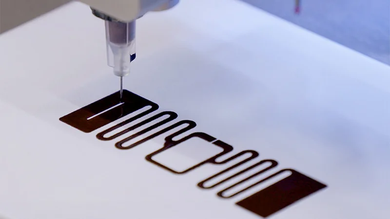
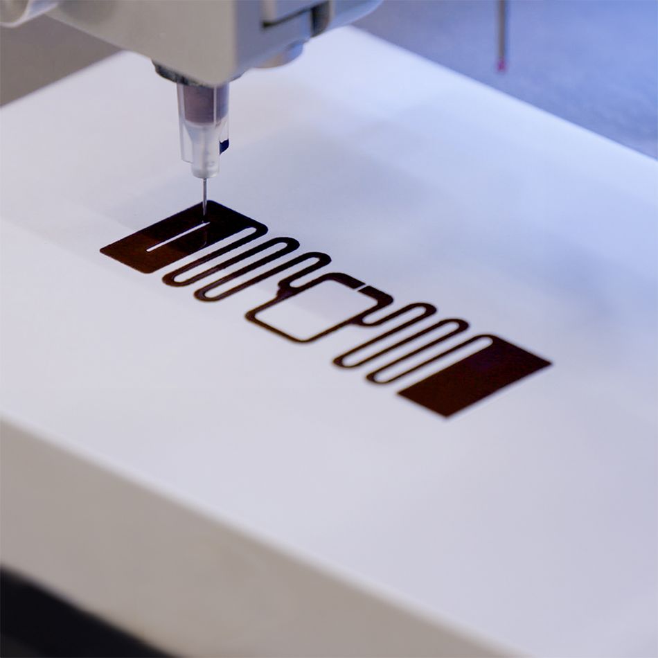
Voltera, together with Jiva Materials, recently hosted a webinar on printing biodegradable PCBs. In the webinar, Chief Product Officer and Founder at Jiva Materials, Jack Herring, presented an overview of Soluboard®, the world’s first fully biodegradable and fully recyclable printed circuit board substrate. Voltera then demonstrated a PCB printed using V-One on Soluboard®. Did you miss it? You can now watch the full webinar on-demand and learn how easy it is to print biodegradable PCBs with Jiva Materials’ Soluboard® and Voltera’s V-One PCB printer:
The environmental cost of traditional PCBs
The environmental impact of the electronics industry has been a significant concern in recent years, as the market for electronic products, including smart devices and IoT appliances, has continued to grow. This ecological impact is both generated by e-waste—one of the fastest growing solid waste streams in the world according to the WHO [2]—as well as through the manufacturing of electronic components, including printed circuit boards.
PCB production specifically has been flagged as an environmental issue for a few reasons. For one, many of the materials currently used in PCBs are non-renewable, including conductive metals like copper, rare earth elements (REE) like neodymium, and epoxy resins. Looking at the life cycle of a PCB, the extraction and mining process for copper ore and REE can’t be ignored: not only are these energy intensive, they result in the pollution of land and water. Moreover, the mass manufacturing of PCBs is also energy intensive, requiring high-temperatures for processes like lamination and the use of industrial equipment that generates harmful emissions.
Perhaps the greatest ecological challenge, however, has come from the disposal and recycling of PCBs. Since the components that make up a PCB—including resin, glass and conductive pathways—are bonded, it is difficult to separate them at the end of the PCB’s life. This has meant that the vast majority of defective or outdated PCBs end up in landfills, making up 42% of e-waste by weight.[3] On top of that, up until very recently, the most viable PCB recycling processes relied on incineration, which not only consumes energy itself, but also generates toxic emissions.
Introducing Soluboard®
Fortunately, there have been recent advances in making PCBs more sustainable. One of these advances comes from UK-based Jiva Materials, which has developed the world’s first fully recyclable PCB substrate, Soluboard®.
Soluboard® is a game-changer in rigid PCB production, offering a carbon footprint reduction of up to 67% compared to more conventional glass-fiber and epoxy substrates. The eco-friendly substrate is made by impregnating natural, degradable fibers within a water-soluble polymer along with a halogen-free flame retardant. This results in a composite material that is formed into copper clad laminate panels, which form the base of PCBs.
The Soluboard® substrate can be used in PCB production workflows, using techniques like water-based etching, electroplating or printing technologies like Voltera’s direct-ink-writing (DIW), as well as curing, drilling, and more. At the end of the PCB’s life, the board can simply be placed in hot water (within a controlled environment), where the substrate will dissolve, making it easier to recover reusable materials, like copper, rare minerals, and the natural fiber. These materials can then be reused in the production of new PCBs.
The Benefits of Soluboard®:
Made from biodegradable non-toxic materials
Facilitates recovery of non-renewable materials, like copper and rare minerals
Compatible with standard processes like water-based etching, electroplating, drilling, routing, and soldering (including low temperature soldering)
Compatible with Plated Through Hole (PTH)
Demonstrates flame retardancy rating equivalent to UL94 V1
Reduces carbon footprint by 67% compared to FR4 substrates
Voltera’s contribution to sustainable printed electronics
Other solutions, like Voltera’s aforementioned DIW printing systems, are also playing a key role in the development of more sustainable PCBs. The company’s flagship novel electronics printing platform, NOVA, uses a precision dispensing system to selectively deposit conductive or dielectric inks onto a wide variety of substrates. This solution not only enables users to rapidly iterate electronic devices—such as sensors and wearables—to accelerate development, but also supports materials research and serves as a key tool in the development of more sustainable PCB materials and devices.
For example, NOVA is a great tool for testing the compatibility between sustainable substrates—such as the rigid Soluboard® or flexible substrates like paper and PET—and printable materials, including those at the cutting-edge of sustainable electronics, like carbon and graphene-based formulations. Researchers can therefore use Voltera’s technology to explore how these materials perform together and to develop new applications that support more sustainable electronics.
A number of Voltera customers are currently investigating the use of self-healing materials to make electronics that can heal themselves when a defect occurs. For instance, a research team at Polytechnique Montreal is using the Voltera’s products to develop self-healing, stretchable and recyclable polyurethane-PEDOT:PSS materials, which could have applications in biosensing and pressure sensing.[4] The Bao Group at Stanford is also working with the V-One PCB printer to develop self-healing robotic skins.[5] The sustainable impact of this capability could be massive down the line, as PCBs and sensors could have longer lifespans, directly minimizing e-waste.

Voltera’s NOVA and V-One platforms offer additional sustainability benefits, including minimized material usage and waste resulting from the additive deposition approach. Since this method deposits material only where needed, there is far less waste than more conventional processes like etching, which is subtractive.
The desktop printing solutions also allow R&D labs and electronic developers to bring their prototyping in-house, eliminating reliance on third-party manufacturing and the emissions associated with shipping. On top of that, by directly printing electronic circuits based on digital designs, Voltera’s solutions eliminate the need for PCB screens and other tooling, further lowering the environmental impact.
References
[1] Global e-Waste Monitor 2024: Electronic Waste Rising Five Times Faster than Documented E-waste Recycling [Internet]. United Nations Institute for Training and Research, 2024. https://unitar.org/about/news-stories/press/global-e-waste-monitor-2024-electronic-waste-rising-five-times-faster-documented-e-waste-recycling
[2] Electronic waste (e-waste) [Internet]. World Health Organization. October 1, 2024. https://www.who.int/news-room/fact-sheets/detail/electronic-waste-(e-waste)
[3] Chakraborty M, Kettle J, Dahiya R. Electronic waste reduction through devices and printed circuit boards designed for circularity. IEEE Journal on Flexible Electronics. 2022 Jan;1(1):4-23.
[4] Kim J, Fan J, Petrossian G, Zhou X, Kateb P, Gagnon-Lafrenais N, Cicoira F. Self-healing, stretchable and recyclable polyurethane-PEDOT: PSS conductive blends. Materials Horizons. 2024;11(15):3548-60.
[5] Next generation electronics with Voltera [Internet]. Voltera, 2025. https://www.voltera.io/use-cases/customer-stories/stanford-university