Blank PCB Technology: Technical Guide for Engineers and Designers
This technical guide explores the various types, material properties, manufacturing processes, and key design considerations associated with blank PCB technology!

17 Jun, 2025. 22 minutes read
Bare Board, Blank PCB Technology
Introduction
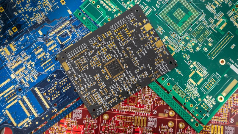
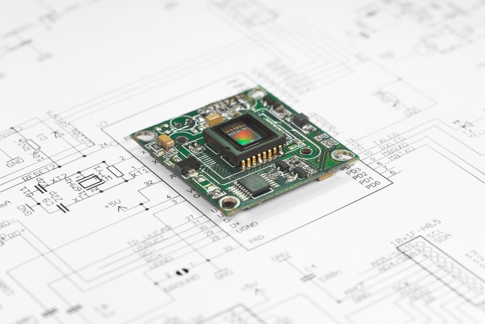
The journey of any electronic device begins with a blank PCB, a seemingly simple yet critical starting material, providing the essential platform for interconnecting components. It is frequently termed as a 'copper-clad' circuit board because it typically consists of a non-conductive substrate material with one or more thin layers of copper foil bonded to its surface(s). This copper layer is the raw material from which conductive traces will later be patterned.
If you’re developing consumer electronics, industrial control systems, or embedded solutions, an adequately designed blank PCB ensures electrical reliability and optimal layout flexibility. This technical guide explores the various types, materials, manufacturing processes, and key design considerations associated with blank PCB technology!
Understanding the Blank PCB: Core Concepts and Terminology
What is a Blank PCB (Bare PCB, Copper-Clad Laminate - CCL)?
A blank PCB, also known as a bare PCB or copper-clad laminate (CCL), represents the unprocessed, foundational stage of any printed circuit board. It consists of a non-conductive substrate, typically FR-4 or similar material, laminated with one or more layers of copper foil. This copper layer is critical for forming the circuit traces that enable electrical connections. The blank PCB provides both mechanical support and the platform for conducting paths, making it essential to any PCB design or fabrication process.
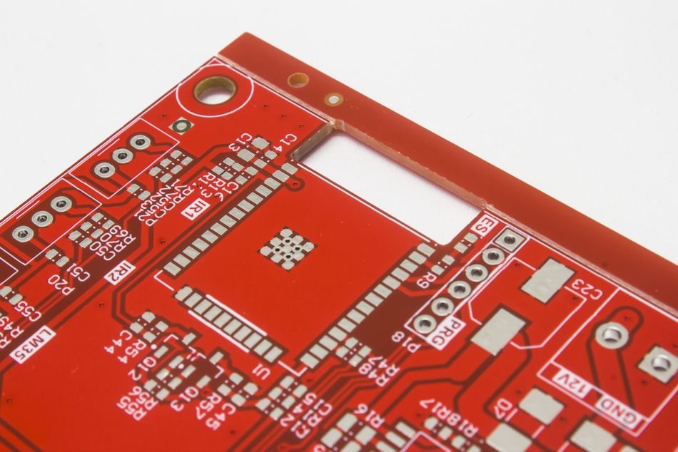
Engineers utilize the blank PCB as the initial platform or "canvas" for creating specific electronic circuits. Through processes like etching, parts of the copper are removed to develop defined routing paths and pads. The type of substrate, copper thickness, and laminate quality directly impact thermal performance, electrical reliability, and PCB manufacturing outcomes. Thus, selecting an appropriate blank PCB is a critical first step in the circuit design and manufacturing workflow.
Brief Historical Perspective on PCB Development
The journey to the modern blank PCB reflects the broader evolution of electronic technology. Early electronics relied on point-to-point wiring, which was bulky and prone to failure. Innovators like Albert Hanson and Charles Ducas introduced multi-layer and conductive ink techniques, paving the way for modern boards. In 1941, Paul Eisler developed the first practical blank printed circuit board using copper-clad material and the etching process. This method experienced rapid adoption during World War II, particularly for compact and rugged military electronics. [1]
Post-war, blank PCB technology gained momentum with the introduction of consumer devices, such as transistor radios. The advancements in soldering, laminate processing, and mass production techniques supported the rise of single-sided, double-sided, and eventually multilayer PCBs. Today, the blank PCB remains a cornerstone in electronics, powering everything from DIY projects to aerospace systems.
Recommended Reading: Bare Board Technology: Everything You Need to Know
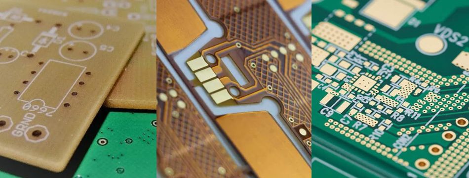
The Anatomy of a Blank PCB: Key Materials and Their Properties
Substrate Materials: The Insulating Backbone
The substrate is the dielectric material that forms the core of the blank PCB, separating the conductive copper layers and providing the necessary mechanical rigidity or flexibility. Its properties are critical as they influence not only the structural integrity of the board but also its electrical performance, particularly how signals propagate. Its dielectric constant, dissipation factor, thermal conductivity, and CTE affect signal integrity, EMI, and heat management.
Substrate selection is a crucial step in PCB design, as it involves balancing electrical, mechanical, and cost factors.
FR-4
FR-4 (Flame Retardant Level 4) is the most widely used substrate material for blank PCBs, due to its excellent balance of cost-effectiveness, mechanical strength, and electrical insulation properties.
Composition: It is a composite material made from woven fibreglass cloth impregnated with an epoxy resin binder that includes flame-retardant additives.
Properties: FR-4 exhibits good mechanical robustness, with typical tensile strength ranging from 310 to 440 MPa and flexural strength around 480 MPa. Its electrical properties are suitable for many general-purpose applications, with a dielectric constant typically ranging from 4.0 to 4.8 and a dissipation factor of around 0.015 to 0.025. However, its thermal conductivity is relatively low, typically ranging from 0.3 to 0.4 W/mK, which can be a limitation in high-power applications. [2]
Applications: FR-4 is the workhorse material for a vast array of electronic devices, including consumer electronics (smartphones, laptops), industrial control systems, power supplies, and automotive electronics.
Limitations: While versatile, standard FR-4 is generally not suitable for very high-frequency applications (typically above 1 GHz) due to its relatively high dielectric frequency-dependent dissipation factor loss, which leads to significant signal loss.
High-Frequency Laminates
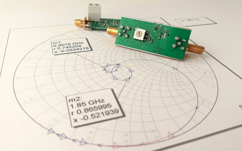
For applications operating in the radio frequency (RF) and microwave spectrum, or those involving very high-speed digital signals, specialized laminate materials are necessary to maintain signal integrity and minimize losses.
1. Rogers Materials (e.g., RO4350B, RO3000 series)
Composition: These materials are often hydrocarbon-ceramic laminates or Polytetrafluoroethylene (PTFE)-based composites. For instance, RO4350B is a glass-reinforced hydrocarbon/ceramic thermoset material.
Properties: Rogers materials are characterized by excellent high-frequency performance, primarily due to their low dielectric constant that remains stable across a wide range of frequencies, and a very low dissipation factor. They also offer superior temperature stability (RO4350B has a Tg greater than 280°C), low moisture absorption, and often better thermal conductivity compared to FR-4 (RO4350B thermal conductivity is around 0.69 W/mK).
Applications: These materials are indispensable for RF and microwave circuits, antennas, satellite communication systems, automotive radar, and high-speed digital designs where signal integrity is paramount.
2. PTFE (Teflon) Substrates
Composition: Based on Polytetrafluoroethylene, often reinforced with woven glass or ceramic fillers to improve mechanical stability.
Properties: PTFE substrates boast an extremely low dielectric constant (typically around 2.1 to 2.5) and a very low dissipation factor, making them ideal for minimizing signal loss at very high frequencies. They also exhibit excellent thermal stability over a wide temperature range (from cryogenic temperatures up to +260°C), high chemical resistance, and very low moisture absorption. However, PTFE is mechanically softer than FR-4 and can present challenges during fabrication, such as drilling and plating adhesion.
Applications: Widely used in high-frequency RF circuits, microwave communication systems, satellite electronics, 5G and beyond communication technologies, aerospace, and military applications where minimal signal attenuation and high performance are critical.
Polyimides
Polyimide materials are a class of polymers known for their exceptional thermal stability and mechanical properties, making them suitable for demanding applications, including flexible circuits.
Composition: These are aromatic heterocyclic polymers.
Properties: Polyimides offer excellent thermal stability, with glass transition temperatures (Tg) often exceeding 250°C to 300°C, and maximum operating temperatures above 260°C. They possess good mechanical strength (tensile strength of 200-300 MPa) and are inherently flexible, which is crucial for dynamic applications and flex PCBs. However, they tend to absorb more moisture than FR-4, which may necessitate pre-baking before assembly.
Applications: Polyimides are the primary material for flexible PCBs (FPCs) and rigid-flex PCBs. They are also used in rigid PCBs for high-temperature environments found in aerospace, military, medical implantable devices, and particular automotive applications.
CEM (CEM-1, CEM-3)
Composite Epoxy Materials (CEM) offer alternatives to FR-4, particularly in cost-sensitive applications.
Composition:
CEM-1: Features a cellulose paper core sandwiched between layers of woven glass fabric, all impregnated with a flame-resistant epoxy resin.
CEM-3: Consists of a chopped glass fibre core with woven glass fabric surfaces, also using an epoxy resin. It is often described as being similar to FR-4 but utilizes 'flies' (short glass fibres) in the core instead of continuous woven glass.
Properties:
CEM-1: Generally cheaper than FR-4, especially for single-layer blank PCBs. It has weaker flexural strength and a higher CTE compared to FR-4 but offers good punchability, making it suitable for high-volume, low-cost single-layer board manufacturing. It is limited to single-layer applications because its paper core is not ideal for plated-through holes.
CEM-3: Presents a milky white, smooth appearance and is flame-retardant. It can serve as a cost-effective alternative to FR-4 for double-sided and some multilayer PCBs, offering better electrical properties than older paper-based materials, such as FR-2.
Applications:
CEM-1: Commonly found in single-sided PCBs for consumer electronics like toys, remote controllers, household appliances, and some LED lighting applications.
CEM-3: Used in double-sided and less demanding multilayer PCBs where cost is a significant driver, such as in some white goods and automotive electronics.
Metal Core PCBs (MCPCBs/IMS)
Metal Core Printed Circuit Boards (MCPCBs), also known as Insulated Metal Substrates (IMS), are specifically designed for applications that require efficient heat dissipation.
Composition: An MCPCB typically comprises a metal base plate (most commonly aluminium, but copper can also be used), a thin layer of thermally conductive but electrically insulating dielectric material, and a copper circuit layer on top.
Properties: The primary advantage of MCPCBs is their excellent thermal management capability. The metal core acts as a heat sink, efficiently dissipating the heat generated by electronic components. Aluminium offers a good balance of thermal conductivity, light weight, and cost-effectiveness. Copper core MCPCBs provide even better thermal performance (copper conductivity ~400 W/mK) but are heavier and more expensive. MCPCBs also offer good mechanical stability and can reduce the need for separate heat sinks.
Applications: MCPCBs are widely used in LED lighting, power supply modules, automotive electronics, motor drives, and solid-state relays, where efficient thermal dissipation is crucial for optimal performance and longevity.
Recommended Reading: Metal Core PCB (MCPCB): Revolutionizing Thermal Management in Electronics
Ceramic Substrates (Alumina, AlN)
Ceramic substrates are employed in applications demanding very high thermal conductivity, excellent electrical insulation at high temperatures, and stability in harsh environments.
Composition:
Alumina (Aluminium Oxide, Al2O3): A commonly used ceramic material.
Aluminium Nitride (AlN): A higher-performance ceramic known for its exceptional thermal conductivity.
Properties:
Alumina: Offers good thermal conductivity (typically 20-30 W/mK), high dielectric strength, high rigidity (though it can be brittle), and a dielectric constant around 9-10. It is more cost-effective than AlN.
Aluminium Nitride (AlN): Provides superior thermal conductivity (ranging from 170 W/mK to over 230 W/mK), making it excellent for very high-power applications. It also features a strong dielectric strength, a low CTE that closely matches silicon, high operating temperature capability, and a dielectric constant around 8.8-9.0. AlN is generally more expensive than alumina.
Applications: Ceramic blank PCBs are used in high-power LED modules, RF power amplifiers, high-temperature sensors, automotive electronics, aerospace, and military systems where robust thermal management and environmental stability are crucial.
The wide variety of substrate materials reflects the evolving demands of PCB circuit board technology. FR-4 dominates due to its general-purpose versatility; however, high-frequency, metal-core, and ceramic substrates are essential for specialised needs. Selecting the right blank PCB material impacts everything—from soldering methods to PCB assembly, performance, and system longevity.
Recommended Reading: PCB Materials: A Comprehensive Guide to Understanding and Choosing the Right Materials
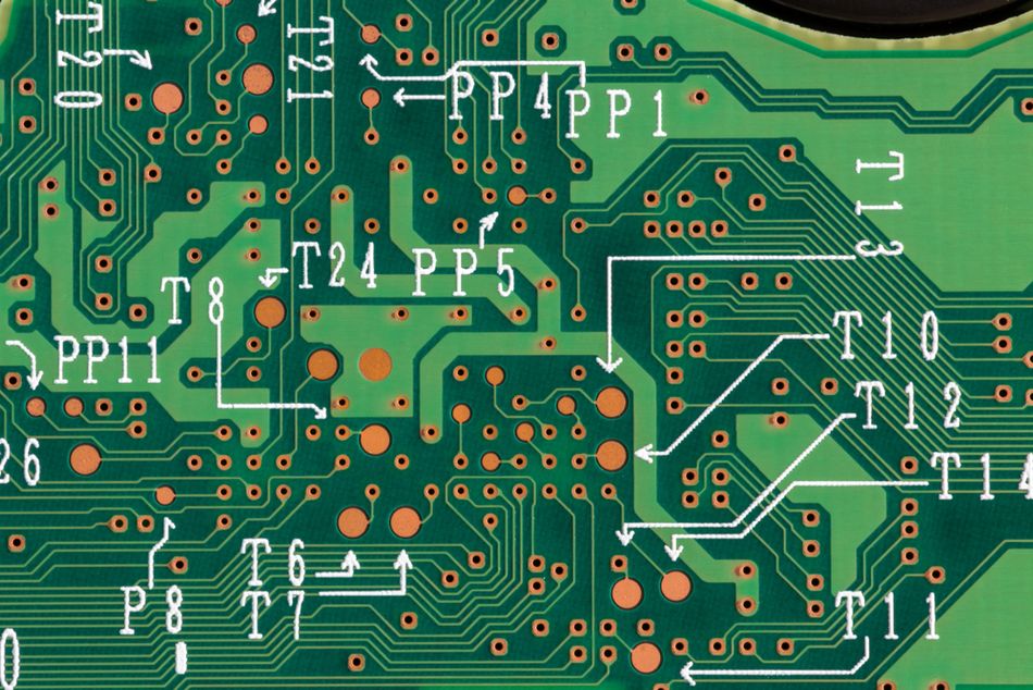
Copper Foil: The Conductive Pathways
The copper foil laminated onto the substrate of a blank PCB is the material from which all conductive elements—traces, pads, and planes—are ultimately formed.
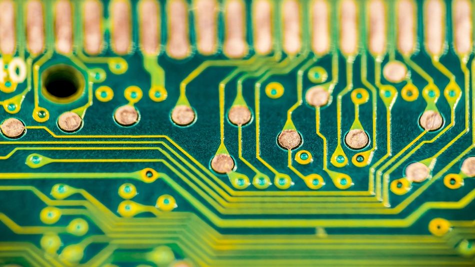
Its characteristics are vital for the electrical and mechanical performance of the final circuit. The quality, type, and thickness of this copper foil are critical parameters.
Types of Copper Foil: Electro-Deposited (ED) vs. Rolled-Annealed (RA)
There are two primary types of copper foil used in blank PCB fabrication, distinguished by their manufacturing process and resulting microstructure:
Electro-Deposited (ED) Copper: Produced by electroplating copper onto a drum from a copper sulfate solution, ED copper has a columnar grain structure. It offers good adhesion (thanks to its rougher matte side), is cost-effective, and is widely used in rigid blank PCB boards. However, it’s less flexible and not ideal for bending applications.
Rolled-Annealed (RA) Copper: Manufactured by rolling and heat-treating copper ingots, RA copper has an elongated, uniform grain structure. It is smoother, more flexible, and better suited for flexible PCBs and high-frequency circuits where low surface roughness minimizes signal loss.
Essential Copper Foil Properties
Several key properties of copper foil determine its suitability for a given blank PCB application:
Thickness (Copper Weight): Measured in oz/ft², standard weights include 0.5 oz (17.5 µm), 1 oz (35 µm), and 2 oz (70 µm). Thicker foils (e.g., 3 oz or more) are used in heavy copper PCBs for higher current handling and improved heat dissipation. The thickness directly impacts the current-carrying capacity of traces and their thermal performance.
Purity: High-purity copper (≥99.7%) ensures excellent electrical and thermal conductivity, and consistent etching behavior during PCB circuit board fabrication. [3]
Surface Roughness: A rougher surface enhances adhesion (peel strength), but increases conductor loss in high-frequency circuits. For RF or high-speed designs, smooth RA foils or treated ED foils are preferred to reduce skin effect losses.
Conductivity: Copper is chosen for its excellent electrical and thermal conductivity, second only to silver among common metals. These properties are fundamental to its role in efficiently transmitting electrical signals and dissipating heat.
Peel Strength: Peel strength measures the bond between copper and laminate. It affects reliability during soldering, rework, or flexing. Factors influencing peel strength include surface treatments, resin type, and lamination parameters.
Below is the copper weight to thickness conversion table:
| Copper Weight (oz/ft²) | Thickness (µm, approx.) | Thickness (mils, approx.) |
| 0.5 oz | 17.5 | 0.7 |
| 1 oz | 35 | 1.4 |
| 2 oz | 70 | 2.8 |
| 3 oz | 105 | 4.2 |
| 4 oz | 140 | 5.6 |
Choosing between ED and RA copper is more than a conductivity issue! In flexible PCB applications, ductility is vital. In RF and high-speed designs, surface smoothness affects signal quality. Therefore, the selection of copper foil must be aligned with both the substrate choice and the circuit function.
Prepreg: Bonding Layers in Multilayer Blank PCBs
In the construction of multilayer blank PCBs, prepreg plays a pivotal role as the bonding agent and insulating material between conductive layers. Prepreg is a glass-fibre cloth pre-impregnated with partially cured epoxy or polyimide resin. In the lamination process, the resin cures under heat and pressure, bonding layers and forming an insulating barrier between copper layers. It contributes to mechanical strength, defines spacing between layers, and influences impedance in high-frequency circuits.
Primary Functions of Prepreg in Blank PCB Stackups
Bonding: The B-stage resin flows and adheres to adjacent copper foil and substrate surfaces. Upon curing to the C-stage, it permanently bonds the layers.
Dielectric Insulation: The cured prepreg forms a solid dielectric layer, providing electrical insulation between the copper layers it separates.
Mechanical Support: The fibreglass reinforcement within the prepreg contributes to the overall mechanical strength and dimensional stability of the final blank PCB structure.
Thickness Control: Prepreg thickness helps control spacing between signal layers—critical for impedance control in high-speed designs.
Types of Prepreg and Their Characteristics:
Resin System: The type of resin used (e.g., standard FR-4 epoxy, high-Tg epoxy, polyimide, cyanate ester, PTFE composites) dictates the thermal properties of prepreg (Tg, Td), electrical performance (Dk, Df), and chemical resistance. Polyimide prepregs are used for high-temperature applications or flexible sections, while PTFE-based prepregs are chosen for their low dielectric loss in RF circuits.
Glass Style/Weave: The fibreglass cloth comes in various weave styles (e.g., 106, 1080, 2116, 7628, identified by industry codes) and aerial weights (grams per square meter). Looser weaves might lead to more resin-rich areas and potentially less uniform Dk.
Fillers: Inorganic fillers, such as silica, alumina, or boron nitride, can be incorporated into the resin system to modify specific properties. Fillers can help reduce the CTE for better dimensional stability, enhance thermal conductivity for improved heat dissipation, or adjust the dielectric constant and dissipation factor.
Key Properties: Manufacturers specify prepregs by their characteristics, including resin content, resin flow, gel time, cured thickness, Tg, Dk, and Df.
Prepreg is a precision dielectric that directly affects electrical performance and structural reliability. In high-speed digital and RF designs, prepreg properties influence impedance, signal integrity, and through-hole durability. Therefore, prepreg selection must be closely aligned with the chosen substrate, copper foil, and the electrical demands of the blank PCB. It is a critical part of both Design for Manufacturability (DFM) and Design for Reliability (DfR).
Recommended Reading: PCB Prepreg vs Core Materials: Engineering Guide to Laminate Selection and Properties
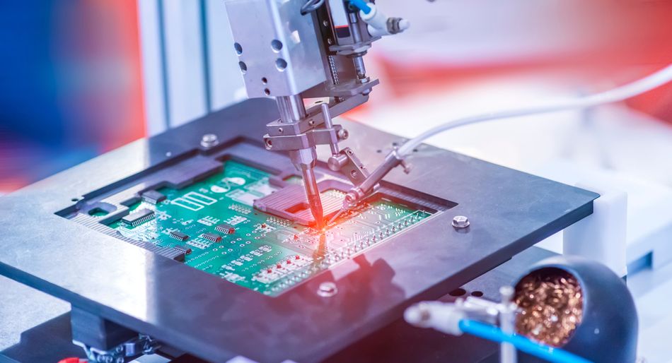
Making of Blank PCB: Copper-Clad Laminate (CCL) Manufacturing
The CCL process begins by impregnating reinforcement materials with a resin system to form prepreg, which is then laminated with copper foil under heat and pressure. The result is a rigid or flexible blank PCB board—ready for PCB design, drilling, etching, and soldering.
Key Raw Materials
The quality and characteristics of a blank PCB are intrinsically linked to its constituent raw materials:
1. Resins
Define thermal and electrical properties (Tg, Td, Dk, Df)
Standard Types: epoxy (for FR-4), polyimide, PTFE, cyanate ester
Modified versions improve flame retardancy, heat stability, or low-loss performance
2. Reinforcements
Most commonly woven fibreglass (e-glass)
Alternatives: glass felt, paper (in CEM-1), or aramid for strength
Weave style affects dimensional stability and dielectric uniformity
3. Copper Foil
Typically high-purity ED or RA copper
Must meet specs for copper weight, surface roughness, and adhesion treatments
Key Manufacturing Steps
1. Resin Mixing
Resins are combined with solvents, catalysts, and additives to form a varnish with controlled viscosity.
2. Impregnation
Rolls of fibreglass cloth are saturated in the resin bath, absorbing the desired resin content.
3. Drying (B-Stage)
Impregnated cloth is passed through ovens, evaporating solvents, and partially curing resin to the “B-stage.”
4. Cutting and Inspection
B-stage prepreg is cut to sheet form and inspected for uniformity, defects, and thickness accuracy.
5. Lay-Up
The layers of prepreg are stacked with copper foil:
Single Sided: Copper Foil / Prepreg / Press Plate
Double Sided: Copper Foil / Prepreg / Copper Foil
Multilayer Core includes internal patterned layers
6. Lamination
The lay-up stack is pressed under high heat and pressure. The B-stage resin flows, fills voids, and cures (C-stage), bonding all layers permanently. Lamination parameters (temp, pressure, duration) critically affect final mechanical and electrical properties.
The performance of a blank PCB depends on the precision of every manufacturing step, from substrate selection to copper adhesion. Poor control can lead to warping, delamination, inconsistent dielectric properties, or failures in PCB assembly. Therefore, sourcing CCLs from certified, quality-driven manufacturers is critical for reliability in high-frequency, multilayer PCB, or double sided PCB applications.
Recommended Reading: How to Make a PCB: Theoretical Concepts and Practical Implementation
Categorizing Blank PCBs: Types and Structures
Based on Layer Count
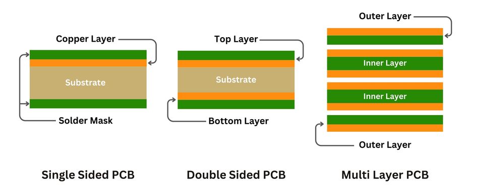
Feature a single copper foil layer laminated to one side of the substrate.
Used for simple circuitry, prototyping, and low-density layouts.
Common in consumer devices, basic electronic circuits, power modules, and DIY projects.
Advantages: Cost-effective, easy to manufacture.
Limitations: Limited routing space, no via interconnections.
Have copper layers on both sides of the dielectric substrate.
Enable more complex routing using plated-through holes (PTHs).
Support moderate circuit density while remaining cost-efficient.
Widely used in power supplies, audio devices, and industrial electronics.
Consists of three or more copper layers, separated by prepreg and core layers.
Allow dense signal routing, controlled impedance, and better EMI shielding.
Ideal for advanced systems such as computers, medical devices, and aerospace electronics.
Tradeoff: Higher fabrication cost and complexity.
Based on Rigidity
Built on FR-4, CEM, metal core, or ceramic substrates.
Offer excellent mechanical strength and are the industry standard for most electronic devices.
Typically used in applications that demand stability and durability.
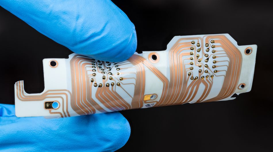
Constructed from polyimide or PET substrates.
Designed to bend, twist, or fold—functional for compact or dynamic assemblies.
Reduce weight, save space, and eliminate the need for connectors between sections.
Challenges: Higher material costs, limited layer count, and stricter routing constraints.
Integrate rigid and flexible sections in a unified board.
Eliminate connectors between segments and improve assembly reliability.
Used in wearables, medical devices, aerospace, and other compact, vibration-prone environments.
Require precise material coordination and specialized PCB manufacturing processes.
Specialized Blank PCBs
1. High-Frequency Blank PCBs
Use low-loss substrates, such as Rogers or PTFE.
Optimized for RF, microwave, and high-speed digital signals.
Key for telecom infrastructure, radar, and satellite systems.
Built with an Alumunium or copper core for efficient thermal conductivity.
Common in LED lighting, motor controllers, and power electronics.
Enhance heat dissipation without the need for external heat sinks.
3. Ceramic Blank PCBs
Made with alumina or Alumunium nitride (AlN) substrates.
Withstand extreme heat, high power, and harsh environments.
Used in automotive, military, and high-frequency RF modules.
Choosing the right blank PCB type affects every aspect of development. For instance, selecting a flexible blank PCB requires attention to polyimide stackups, bend-radius limits, and soldering support. A rigid-flex design alters not just the layout but the entire interconnect strategy.
Thus, blank PCB classification isn’t just technical labeling—it’s a core design decision that shapes circuit complexity, manufacturability, and final product reliability.
Recommended Reading: Types of Printed Circuit Boards: A Comprehensive Guide
From Blank PCB to Functional Circuit: Design and Implementation
Selecting the appropriate Blank PCB: Material Selection
Choosing the correct blank PCB is arguably one of the most crucial decisions in the early stages of electronic product development. The material properties of the substrate, copper foil, and prepreg (in multilayer boards) must align with the specific demands of the application.
Matching material properties to application needs includes:
High-Speed Digital & RF/Microwave Applications: For circuits operating at high frequencies or requiring fast signal rise times, the primary material considerations are a low and stable Dielectric Constant (Dk) and a low Dissipation Factor (Df). Materials like Rogers (e.g., RO4000 series, RO3000 series), PTFE (Teflon), and specialized low-loss FR-4 variants are preferred to minimize signal attenuation, dispersion, and impedance variations.
Power Electronics and High Thermal Load Applications: In designs where significant current is handled or substantial heat is generated (e.g., power supplies, motor drives, high-power LEDs), the blank PCB material must offer excellent thermal conductivity (k) for efficient heat dissipation, a high Decomposition Temperature (Td) to withstand operating temperatures, and appropriate copper weight for current carrying capacity. Metal Core PCBs (MCPCBs) with aluminium or copper bases, and ceramic substrates (Alumina, AlN) are common choices.
High-Temperature Environments: For applications exposed to elevated operating temperatures or requiring survival through harsh thermal cycling, materials with a high Glass Transition Temperature (Tg) and high Td are essential. Polyimides, high-Tg FR-4 grades, and ceramic substrates are suitable options.
Flexible and Rigid-Flex Applications: When the circuit needs to bend, fold, or conform to non-planar surfaces, polyimide is the dominant substrate material for the flexible sections of the blank PCB due to its excellent flexibility, thermal stability, and mechanical durability.
Cost-Sensitive and General-Purpose Applications: For a wide range of consumer electronics and industrial products where performance requirements are moderate and cost is a primary driver, standard FR4 PCB offers the best balance of properties and affordability. CEM (Composite Epoxy Material) types like CEM-1 (for single-sided) and CEM-3 can also be considered as lower-cost alternatives in some cases.
Essential Design Considerations for Engineers
Once a suitable blank PCB material and type are selected, engineers must address several critical design factors to ensure electrical performance, mechanical integrity, and manufacturability.
These include layer stack-up, trace and spacing dimensions, via structures, and Design for Manufacturability (DFM) compliance.
1. PCB Layer Stack-up Design: Principles and Best Practices
The stack-up defines the arrangement of copper layers and dielectric substrates in a multilayer blank PCB. A well-optimized stack-up improves performance in high-speed, power-dense, and EMI-sensitive designs.
Key Objectives:
Controlled Impedance: Achieved by precisely setting dielectric thickness between signal traces and reference planes.
Signal Integrity: High-speed layers should be sandwiched between ground planes (stripline) to reduce crosstalk and EMI.
Power Integrity: Closely spaced power/ground planes form distributed capacitance, stabilizing power delivery.
Manufacturability: Symmetrical stack-ups reduce warpage during lamination and reflow; core and prepreg material compatibility is essential.
Common Stack-up Examples:
4-Layer: Signal / Ground / Power / Signal
6-Layer: Signal / Ground / Signal / Power / Ground / Signal
8+ Layers: Used for complex routing, multiple power domains, and improved shielding.
2. Trace Width, Spacing, and Copper Weight: IPC Standards and Calculations
The dimensions of copper traces on a blank PCB board directly affect current handling, voltage isolation, and thermal reliability.
a. Trace Width vs. Current
Trace width must match the expected current load. Use IPC-2152 to calculate the required width based on copper weight, layer position, and acceptable temperature rise.
b. Copper Weight/Thickness
Standard weights: 0.5 oz, 1 oz, 2 oz
Heavy copper (>3 oz): Used in power electronics, improves heat dissipation. Copper thickness must be specified early in PCB design as it impacts trace width, soldering, and impedance.
c. Trace Spacing (Clearance)
Spacing is determined by:
Voltage level (creepage and clearance)
Signal type (crosstalk risk)
Fabrication capability (e.g., 4/4 mil design limits)
Relevant IPC Standards:
IPC-2221: General guidelines for spacing and trace dimensions
IPC-2152: Modern current-carrying capacity charts
IPC-2222: Specifics for rigid boards
3. Via Technologies: Through-Hole, Blind, Buried, and Microvias
Vias in a blank PCB provide vertical interconnects between layers. Selecting the right type balances signal integrity, density, and cost.
Through-Hole Vias (PTH): Extend through all layers. Cost-effective but uses valuable space.
Blind Vias: Connect outer to inner layers. Improve routing density.
Buried Vias: Connect internal layers only. Ideal for HDI routing without affecting surface space.
Microvias: Laser-drilled, ≤150 µm. Used in HDI PCBs with fine-pitch BGA packages. May be stacked or staggered.
Filled Vias: Epoxy or conductive paste-filled for via-in-pad designs or thermal transfer.
Tradeoff: Advanced via technologies increase fabrication complexity, cost, and lamination cycles.
4. Design for Manufacturability (DFM) from a Blank PCB Perspective
DFM principles ensure that the blank PCB and final circuit can be produced reliably and at scale.
Best Practices:
Early Fabricator Consultation: Understand limits on material types, trace/space, drill sizes, and layer counts.
Material Compatibility: Match blank PCB materials to fabricator capabilities (e.g., certain polyimide or ceramic laminates may require special handling).
Balanced Copper Distribution: Avoid warpage by keeping copper weights and densities symmetric across layers. Use copper thieving if needed.
Annular Ring Sizing: Maintain a minimum annular ring around drilled holes as per IPC-2221 to ensure via plating reliability.
Thus, the blank PCB is not a passive layer—it actively shapes stack-up decisions, via strategy, routing density, and performance outcomes. An integrated design approach—considering material, layout, and DFM constraints from the start—ensures that electrical, thermal, and mechanical requirements are met without costly redesigns.
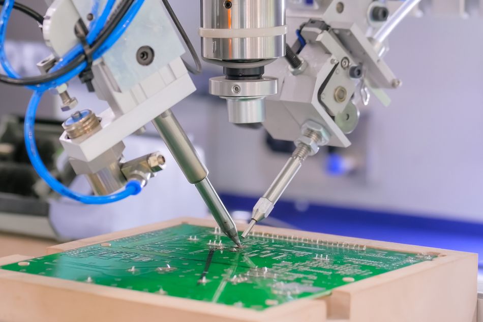
Prototyping with Blank PCBs: Techniques for Students and Professionals
Prototyping is a crucial phase in electronic product development, enabling designers to test and validate their circuits before committing to mass production. Blank PCBs serve as the ideal starting point for creating these initial functional models.
The standard prototyping techniques include:
Etching
Etching is a chemical process that selectively removes unwanted copper from the blank PCB to form circuit traces. It involves:
Coating the copper surface with photoresist
Exposing the resist through a circuit mask using UV light
Developing the resistance to protect the desired traces
Submerging the board in an etchant (e.g., ferric chloride)
Removing the remaining photoresist to expose clean copper paths
Advantages:
Low material cost
Suitable for fine-pitch designs
Ideal for single-sided or double-sided prototyping in DIY and educational setups
Limitations:
Involves hazardous chemicals and waste disposal
Requires setup time (artwork, resist, exposure, etc.)
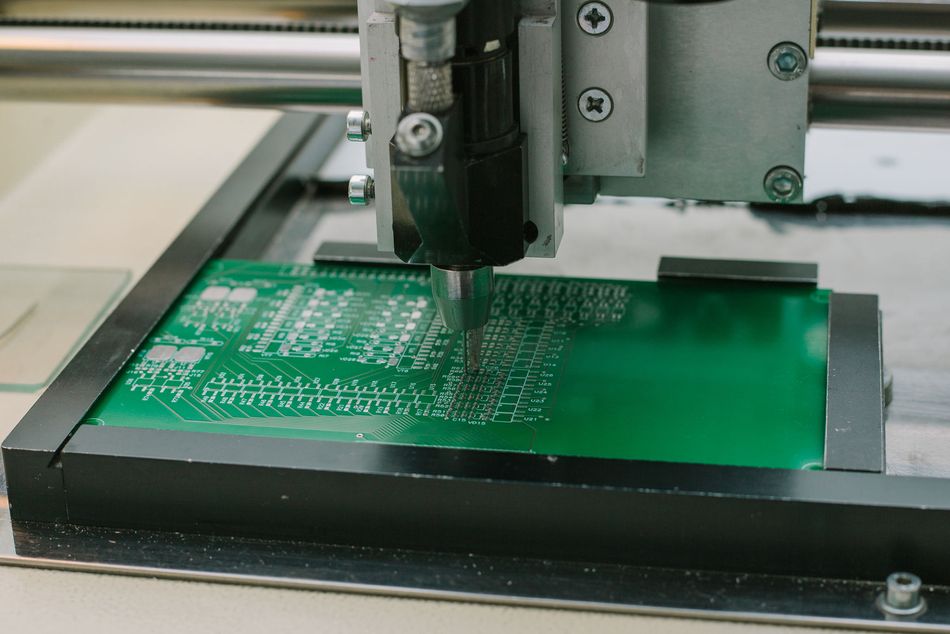
Milling
Milling is a mechanical method using a CNC machine to route isolation paths around copper features. The design is exported from CAD tools to the milling software.
Advantages:
Clean, chemical-free process
Quick turnaround for one-off boards
Compatible with various substrate materials, including FR-4, polyimide, or composites
Limitations:
Equipment cost and tool wear
Limited trace precision due to the tool diameter
Less suited for very fine features or dense layouts
For most prototyping needs, FR-4 blank PCBs are the preferred substrate due to wide availability, low cost, and adequate electrical and thermal performance.
Single-sided FR-4 boards are suitable for basic circuits, while double-sided variants allow more routing flexibility for moderate complexity projects.
Educational Projects Using Blank PCBs
Blank PCBs are an excellent learning tool, especially for students in electronics and engineering programs. Practical prototyping provides exposure to circuit design, component selection, PCB layout, and soldering.
The sample projects include:
LED flasher circuits (e.g., 555 timer)
Sensor interfaces (temperature, LDR, etc.)
Basic linear regulators or power supply modules
Audio amplifiers (e.g., using LM386 or op-amps)
These hands-on exercises help bridge the gap between theory and real-world circuit implementation.
Regardless of the method, the blank PCB remains the universal foundation for early-stage design validation. Whether you're exploring concepts as a student or rapidly iterating in a professional setting, prototyping with blank PCBs allows you to transition from schematic to physical hardware, detect design flaws early, and improve layout and circuit performance before full-scale production.
Recommended Reading: PCB Design: A Comprehensive Guide to Printed Circuit Board Design
Best Practices for Handling, Storage, and Shelf Life of Blank PCBs
While a blank PCB may appear robust, it is a sensitive component whose properties can degrade if not handled and stored correctly. Moisture absorption, contamination, and electrostatic discharge (ESD) are key concerns that can impact manufacturability and the reliability of the final product.
Many dielectric materials used in blank PCBs, particularly epoxy-based resins like those in FR-4, are hygroscopic, meaning they absorb moisture from the ambient environment. Excessive moisture absorption can lead to several problems:
Degradation of Electrical Properties: Moisture can increase the dielectric constant (Dk) and dissipation factor (Df) of the substrate, potentially affecting impedance control and signal integrity in high-speed circuits. It can also lower insulation resistance, increasing the risk of leakage currents.
Delamination and "Popcorning": During high-temperature assembly processes like reflow soldering, trapped moisture can vaporize rapidly, creating internal pressure that leads to delamination (separation of layers), blistering, or "popcorning" (internal voids).
Reduced Tg: Absorbed moisture can lower the glass transition temperature of the resin, making the material more susceptible to deformation at elevated temperatures.
Impact on Solderability: Oxidation or contamination of copper surfaces, exacerbated by moisture, can impair solderability.
IPC-1601A (Printed Board Handling and Storage Guidelines) outlines procedures for moisture-sensitive PCBs, including pre-assembly baking protocols and Moisture Sensitivity Level (MSL) classifications.
Guidelines for Optimal Storage and Maintaining PCB Integrity
Proper storage is essential to preserve the quality and extend the shelf life of blank PCBs:
Environment: Store blank PCBs in a stable, dry environment with controlled temperature, ideally between 15°C and 30°C, and relative humidity (RH) between 40% and 65%. Avoid damp areas and significant temperature fluctuations.
Packaging: For moisture-sensitive materials or long-term storage, blank PCBs should be vacuum-sealed in Moisture Barrier Bags (MBBs) along with desiccant packs and Humidity Indicator Cards (HICs). Anti-static bags or containers should be used to protect against ESD damage, especially for boards that will carry sensitive components. For immersion silver boards, sulfur-free and pH-neutral packaging materials are recommended to prevent tarnishing.
Handling: Minimize direct physical contact with the blank PCB surfaces. Always handle boards by their edges and wear clean, lint-free ESD-protective gloves. Avoid using hand lotions or other products that could transfer contaminants. Transport boards within a facility using appropriate racks, trays, or protective bags. Workstations should be kept clean to prevent Foreign Object Debris (FOD) contamination.
Shelf Life: The usable shelf life of a blank PCB depends heavily on its surface finish and storage conditions.
1. OSP finishes typically have a shorter shelf life (e.g., 6-12 months) and are more sensitive to handling and atmospheric conditions. [4]
2. Metallic finishes, such as ENIG (Electroless Nickel Immersion Gold), Immersion Tin, or HASL (Hot Air Solder Levelling), generally offer longer shelf lives (e.g., 12 months or more) when stored correctly.
3. Proper vacuum packaging and controlled storage environments are crucial for maximising shelf life and ensuring good solderability when the blank PCB is ultimately used. Regular inspection of stored boards and their packaging is advisable.
The blank PCB is more than a passive laminate—it is a precision substrate whose performance hinges on careful environmental control. Treating PCBs with the same attention as sensitive components is crucial for ensuring solderability, electrical stability, and the reliability of the final product. Robust handling and storage protocols, aligned with IPC guidelines, protect your investment from degradation before the first component is even mounted.
Recommended Reading: Supply Chain Resilience For PCB
Future Trends in Blank PCB Technology
Innovations in Advanced Materials and Composites
Ongoing R&D in substrate materials is focused on overcoming the performance and thermal limitations of traditional FR-4 and epoxy-based systems.
Electrical Advancements: New substrates with ultra-low and stable dielectric constants (Dk) and dissipation factors (Df) are enabling support for GHz-range and millimetre-wave designs.
Thermal Enhancements: Composites with ceramic-filled polymers or higher intrinsic thermal conductivity manage heat more efficiently in power-dense systems.
Improved Thermomechanics: Materials with better CTE matching, higher Tg/Td, and resistance to CAF (Conductive Anodic Filament) help improve long-term reliability.
Advanced Resins and Fibres: The use of high-performance polyimides, cyanate esters, and novel reinforcement fabrics is pushing boundaries in both electrical and mechanical durability.
The Role of Blank PCBs in 5G/6G, IoT, and AI
Emerging technologies are placing unique demands on blank PCBA technology:
5G/6G Communications: The rollout of 5G and the development of future 6G systems necessitate blank PCBs capable of handling extremely high frequencies (mmWave) with minimal signal loss and excellent thermal management for active antenna arrays and base station equipment. Substrate-Like PCBs (SLPs), which feature finer line/space capabilities similar to semiconductor substrates, are being adopted for miniaturization in high-end smartphones and other compact 5G devices.
Internet of Things (IoT): The vast and diverse IoT ecosystem requires a wide array of blank PCB types. This includes low-cost, often single or double-sided boards for simple sensors and disposable devices, as well as compact, power-efficient, and sometimes flexible blank PCBs for wearables and integrated modules. Reliability in various environmental conditions is also a key factor.
Artificial Intelligence (AI) and High-Performance Computing (HPC): AI accelerators, powerful processors, and large memory arrays used in AI and HPC systems generate significant heat, requiring extremely high-speed data transmission. This translates to a demand for blank PCBs with high layer counts, sophisticated thermal management solutions (e.g., embedded cooling, high-k materials), superior power integrity, and exceptional signal integrity to support fast data processing and complex interconnections.
Sustainable Solutions: Biodegradable and Recyclable PCBs
Growing environmental concerns about electronic waste (e-waste) are spurring innovation in sustainable blank PCB materials and end-of-life solutions.
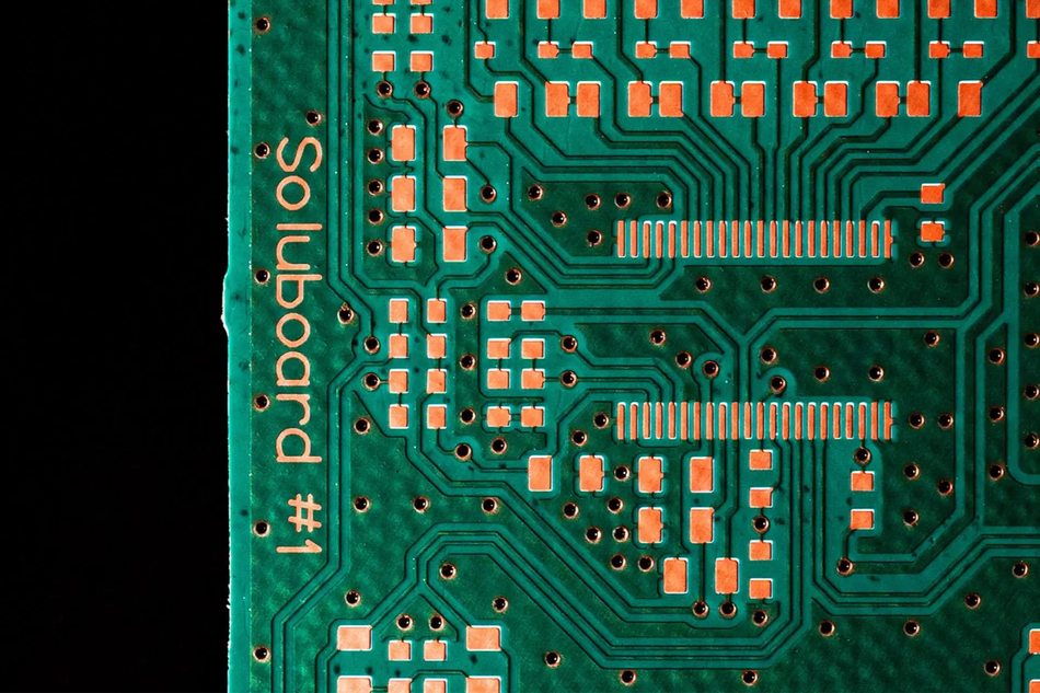
Biodegradable Substrates: Efforts are underway to develop blank PCB substrates that can naturally decompose at the end of their life, reducing landfill burden. Examples include JIVA Materials' Soluboard®, made from natural fibres like flax and jute, which dissolves in hot water, allowing for component and precious metal recovery. Polylactic acid (PLA), derived from organic waste, is also being explored as a biodegradable option for flexible PCBs.
Recyclable Materials and Circular Economy: There is a push towards using more recyclable materials in blank PCB construction and developing better processes for recovering valuable materials from end-of-life boards. This includes initiatives for recycling copper and precious metals, and even investigating the use of recycled tin for soldering processes. Regulatory drivers, such as the German National Circular Economy Strategy, are expected to encourage these trends.
Other Notable Trends:
High-Density Interconnect (HDI) Technology: The drive for miniaturization continues to fuel the adoption of HDI blank PCBs, characterized by microvias, thinner traces and spaces, and sequential lamination techniques. This allows for more connections in smaller areas, supporting compact and powerful devices.
Embedded Components: Integrating passive components (resistors, capacitors) and even active components (ICs) directly within the layers of the blank PCB is a growing trend. This can reduce board size, improve electrical performance (shorter interconnects), and enhance thermal management.
3D-Printed PCBs: Additive manufacturing, or 3D printing, is emerging as a viable technology for PCB prototyping and potentially for customized, low-volume production. It offers the potential for faster turnaround times, complex geometries, and reduced material waste.
Automation and Smart Manufacturing (Industry 4.0): The fabrication of blank PCBs is increasingly benefiting from automation, robotics, AI-driven design optimization, and real-time data analytics. These advancements aim to improve production efficiency, reduce defects, enhance quality control, and enable more agile manufacturing.
Together, these forces are redefining what makes a "superior" blank PCB—not just in terms of speed or reliability, but also lifecycle impact, recyclability, and responsible sourcing. Engineers, material scientists, and manufacturers will increasingly work together to develop holistic solutions that meet performance needs without compromising sustainability.
Conclusion
Blank PCB technology forms the critical foundation of every electronic system, from basic circuits to high-performance computing platforms. With the increasing demands for speed, thermal efficiency, and miniaturisation, engineers must carefully select materials, design layouts, and consider manufacturability early in the design process. With emerging innovations in substrates, via technologies, and sustainable materials, the blank PCB is no longer a passive element—it is a strategic design choice. By aligning technical requirements with best practices in handling, prototyping, and future-proofing, engineers can ensure reliable, high-quality outcomes across diverse applications while also contributing to a more sustainable electronics ecosystem.
Frequently Asked Questions (FAQs)
Q. What’s the difference between a blank PCB, bare PCB, and copper-clad laminate (CCL)?
A. CCL is the raw copper-laminated sheet, whereas a blank or bare PCB is a trimmed, unetched board ready for fabrication, without components.
Q. What is the most common blank PCB material and why?
A. FR-4 is most common due to its low cost, flame resistance, strong insulation, and mechanical durability—ideal for general electronics.
Q. What does copper weight mean on a PCB blank?
A. It indicates copper thickness. "1 oz" equals ~35µm thick copper over 1 sq. ft., affecting current capacity and heat dissipation.
Q. Why is Dk essential in high-speed PCB design?
A. Dk affects signal speed and impedance. Lower, stable Dk ensures minimal distortion, better impedance control, and higher signal integrity.
Q. What are the main prototyping methods for blank PCBs?
A. Etching (chemical) and milling (mechanical). Etching offers precision; milling is cleaner and faster, but it is costlier and less accurate for fine details.
Q. How should I store blank PCBs properly?
A. Keep in 15–30°C, 40–65% RH, sealed with desiccants and HICs. Avoid moisture, dust, and direct contact. Use anti-static gloves and proper packaging.
References
[1] ResearchGate. The Origins and Evolution of the PCB: A Review [Cited 2025 June 10] Available at: Link
[2] Wevolver. FR4: Understanding the Material and Its Applications in PCB Design [Cited 2025 June 10] Available at: Link
[3] Altium. Thermal Conductivity and Thermal Management for Printed Circuit Boards [Cited 2025 June 10] Available at: Link
[4] Cadence. Working With OSP Treated PCBs [Cited 2025 June 10] Available at: Link
in this article
1. Introduction2. Understanding the Blank PCB: Core Concepts and Terminology3. The Anatomy of a Blank PCB: Key Materials and Their Properties4. Making of Blank PCB: Copper-Clad Laminate (CCL) Manufacturing5. Categorizing Blank PCBs: Types and Structures 6. From Blank PCB to Functional Circuit: Design and Implementation7. Best Practices for Handling, Storage, and Shelf Life of Blank PCBs8. Future Trends in Blank PCB Technology9. Conclusion 10. Frequently Asked Questions (FAQs)11. References