What is High Bandwidth Memory 3 (HBM3): Complete Engineering Guide 2025
What is High Bandwidth Memory 3 (HBM3)? This comprehensive engineering guide covers architecture, applications, and performance, along with some advanced techniques used by leading AI companies and best implementation strategies!

30 Jun, 2025. 15 minutes read

High Bandwidth Memory 3 (HBM3) Technology
Introduction
In the rapidly evolving world of high-performance computing, what is High Bandwidth Memory 3 (HBM3) is becoming a central question for engineers, developers, and system architects. HBM3 delivers significant improvements in memory bandwidth, capacity, and power efficiency—making it ideal for AI training, scientific simulations, and advanced graphics processing.
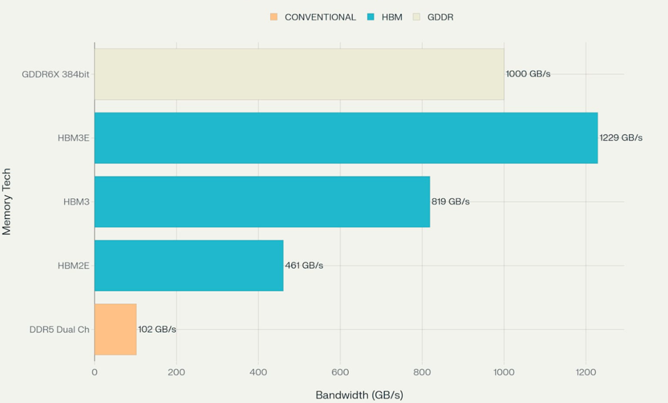
With up to 819 GB/s per stack and support for 64 GB densities, HBM3 sets a new benchmark in memory performance. This article explores what is High Bandwidth Memory 3 (HBM3) from an engineering perspective—covering design principles, use cases, and system optimization techniques. By the end, you’ll have a comprehensive understanding of what is High Bandwidth Memory 3 (HBM3), and its transformative role in next-generation computing systems.
Theoretical Foundations Reveal The Revolutionary 3D Memory Architecture of HBM3
High Bandwidth Memory 3 (HBM3) leverages 3D-stacked DRAM architecture, vertical interconnects, and ultra-wide bus widths to redefine memory throughput, latency, and power efficiency. This innovative memory technology achieves 819 GB/s of memory bandwidth per stack—nearly twice that of HBM2E—while retaining a compact footprint.
This makes it ideal for data centre applications, AI training, and High Performance Computing (HPC) workloads.
Wide Parallelism with Lower Clock Speeds
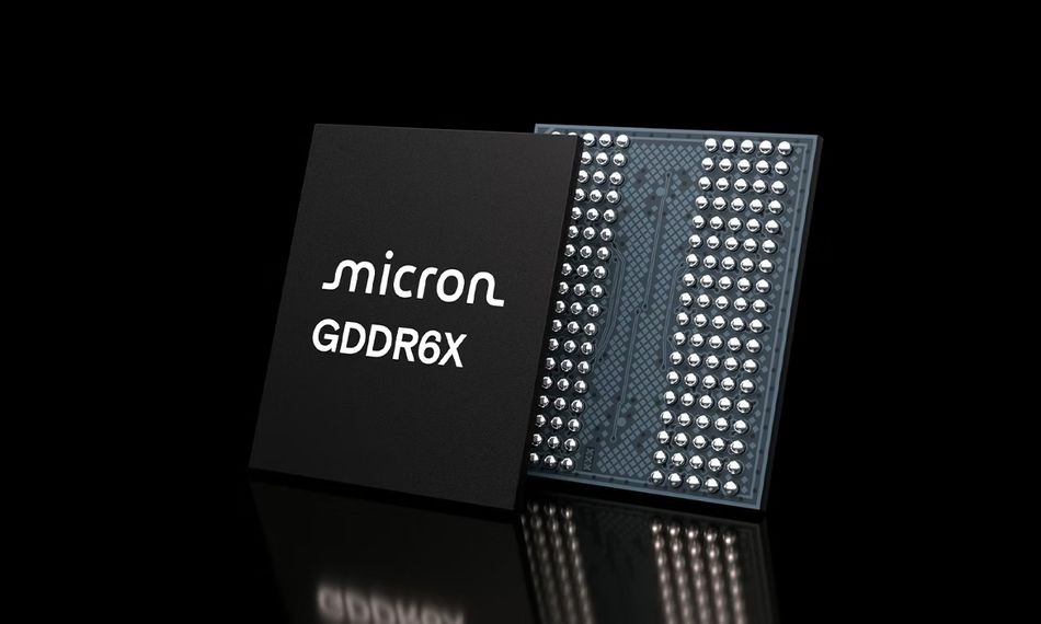
Unlike conventional DDR5 or GDDR6 memory modules, which rely on high clock speeds and narrow channels, HBM3 employs 16 independent 64-bit channels, resulting in a 1024-bit wide interface per stack. This configuration enables high bandwidth at reduced clock frequencies, minimizing power consumption while maintaining throughput. For instance, HBM3 achieves 6.4 Gbps per pin, while GDDR6X, often used in NVIDIA GPUs, requires up to 23 Gbps per pin to match comparable performance.
Bandwidth Efficiency: The Math Behind the Magic
The efficiency of HBM3 memory is best understood through its bandwidth formula:
Total Bandwidth = Data Rate × Interface Width ÷ 8
Applying this to HBM3:
6.4 Gbps × 1024 bits ÷ 8 = 819 GB/s per stack
Compare that to a high-end GDDR6X configuration (e.g., 384-bit interface):
21 Gbps × 384 bits ÷ 8 = 1,008 GB/s total
While GDDR6X offers comparable bandwidth across the entire GPU, HBM3 achieves nearly equivalent throughput per memory stack. It offers a higher bandwidth density, essential for machine learning, large LLMs, and semiconductor accelerators.
Advanced 3D-Stacking: Through-Silicon Vias and TSV Technology
The breakthrough lies in its 3D stacking technology, which vertically integrates up to 12 DRAM dies using Through-Silicon Vias (TSVs)—microscopic (~5–10μm) copper-filled holes that provide direct electrical connections between stacked layers. These TSVs reduce latency, enable lower power signaling, and enhance signal integrity compared to traditional 2D PCB routing.
This approach is a cornerstone of silicon interposer-based designs, where memory stacks and processors (CPUs or GPUs) are mounted on a shared substrate, reducing trace lengths and enabling high-speed interconnects. The result is better power efficiency, higher data rates, and compact system footprints.
Yield Improvements and Manufacturer Advancements
Leading memory manufacturers like SK Hynix, Samsung, and Micron have made major strides in optimizing HBM3 DRAM yields. Current production techniques achieve 80%+ yield rates for 12-high stacks—significantly improved from earlier HBM2 and HBM2E versions.
These improvements are driving down costs and accelerating adoption in AI accelerators, HPC nodes, and next-generation GPUs from AMD and NVIDIA.
Recommended Reading: HBM2 vs GDDR6: Engineering Deep Dive into High-Performance Memory Technologies
Architecture Design Techniques Leverage Advanced 2.5D Packaging Methodologies
Silicon Interposer: The Core of HBM3 Integration
The successful implementation of High Bandwidth Memory 3 (HBM3) relies on advanced 2.5D packaging technologies—most notably, silicon interposer-based integration. Unlike traditional PCB-based memory solutions, HBM3 systems co-locate memory stacks and processors (CPUs, GPUs, or AI accelerators) on a shared interposer that provides ultra-dense interconnects, enhanced signal integrity, and improved power efficiency.

A typical silicon interposer is fabricated using 65nm process technology, capable of routing over 1,700 signal traces between memory and compute dies with sub-10μm precision. This dense routing infrastructure supports the full 1024-bit memory interface at data rates up to 6.4 Gbps, while minimizing latency and signal loss.
Step-by-Step: HBM3 Integration Process
1. Interposer Fabrication:
Manufactured using fine-pitch metal layers and via arrays.
Supports differential routing with impedance control between 40–50 ohms.
Enables parallel signaling across 1024 lanes with <100ps skew.
2. HBM3 Stack Attachment:
Connected using micro-bumps with 73μm pitch for high-density vertical I/O.
Utilizes Through-Silicon Vias (TSVs) to connect 3D-stacked DRAM dies.
Up to 12 DRAM dies per stack for capacities of 16–64 GB.
3. Processor Die Placement:
Requires ±1μm alignment tolerance for functional yield and timing closure.
Integrates memory controller logic close to HBM3 for minimal delay.
4. Package Assembly & Thermal Management:
Advanced cooling and power delivery networks (PDNs) with <1 milliohm impedance.
Includes decoupling capacitors, thermal interface materials, and multi-layer substrates.
Maintains performance across -40°C to +125°C operating range.
Quantitative Advantages of 2.5D Packaging
The adoption of 2.5D packaging in HBM3 architecture brings substantial performance and efficiency gains over traditional PCB-based memory designs. By shortening the interconnect path between memory and processor through a silicon interposer, signal propagation delays are reduced by approximately 40%. This enables faster data transmission and improved overall system responsiveness.
Additionally, power efficiency sees a notable 60% improvement, driven by optimized impedance control and reduced parasitic losses across the high-density interconnects. The design also enhances system reliability, as impedance matching and advanced equalization techniques minimize signal degradation and maintain integrity across the entire 1024-bit wide interface—even under high data rate operations.
Recommended Reading: HBM Memory: Complete Engineering Guide & Design Optimization 2025
Industry Applications Span from Artificial Intelligence to High-Performance Computing
AI and Machine Learning: HBM3 Powers the Future of Model Training
The largest and most transformative use case of HBM3 memory in 2025 is in AI training. For example, H100 GPU by NVIDIA utilizes 80 GB of HBM3, delivering an unmatched 3.35 TB/s of bandwidth. This allows training of GPT-scale models (175+ billion parameters) with 30–50% faster convergence compared to systems using HBM2E or DDR5.
Memory bandwidth becomes the key enabler here, allowing large-scale batch processing, rapid weight updates, and minimal I/O bottlenecks for multi-GPU data center clusters.
High-Performance Computing (HPC): Scientific Accuracy Meets Speed
In HPC workloads, Instinct MI300X by AMD showcases the raw power of HBM3 with 192 GB capacity and 5.3 TB/s bandwidth. This configuration significantly accelerates complex computational tasks such as computational fluid dynamics, quantum chemistry simulations, and molecular orbital calculations. Compared to DDR5-based systems, HBM3 enables up to a 2.5x performance boost, offering lower latency for random-access operations and superior energy efficiency. The system also maintains thermal stability under sustained load, making it ideal for continuous scientific computing applications.
Data Center Deployments: Performance at Scale
HBM3 proves critical to large-scale data center performance at the hyperscale level. For instance, the Llama 3 infrastructure by Meta utilized 16,384 H100 GPUs, each equipped with HBM3, to maintain 90% effective utilization despite hardware faults occurring every 3 hours. This resilience is made possible through the fast recovery protocols of HBM3, built-in ECC capabilities, and low-latency interconnects that support intelligent workload redistribution. These features translated into measurable savings—over $2.5 million annually in electricity costs—due to enhanced power efficiency and system uptime.
Graphics, Visualization, and Real-Time Rendering
In professional visualization, HBM3 DRAM delivers transformative results for real-time graphics and content creation. High-end GPUs equipped with HBM3 enable seamless real-time ray tracing, 8K video editing, and 3D architectural modeling. These systems handle 4x larger scene datasets than GDDR-based solutions, rendering environments with over 500 million polygons in real time. The high memory bandwidth and large capacity support smooth manipulation of high-resolution textures and complex Building Information Models (BIM) without performance degradation.
Cost and Market Positioning
While HBM3 memory carries a premium price tag—approximately $120 per 16 GB stack—it delivers unmatched value for bandwidth-critical workloads. With 8x the bandwidth density of DDR5 and significantly improved performance-per-dollar in demanding environments, HBM3 justifies its cost in semiconductor, GPU, and AI accelerator applications. In 2025, it is consistently integrated into premium computing devices where memory throughput, power efficiency, and system compactness are critical performance differentiators.
Integration with Silicon Interposer Technology Enables Unprecedented Memory Density
System-Level Optimization Through 2.5D Integration
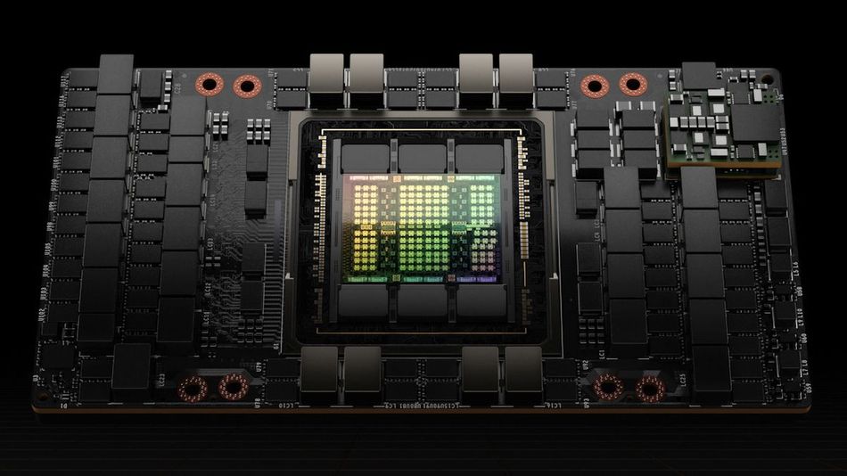
The combination of High Bandwidth Memory 3 (HBM3) and silicon interposer technology marks a pivotal advancement in semiconductor system design, enabling higher memory density, superior thermal performance, and seamless power distribution. This 2.5D integration allows multiple HBM3 stacks to share a unified Power Delivery Network (PDN) and thermal management infrastructure while preserving independent memory channels.
Practical Integration: TSMC CoWoS-S Case Study
A leading example of this integration is CoWoS-S platform by TSMC, which accommodates up to 8 HBM3 stacks on a single interposer measuring 858 mm². This architecture supports an aggregate bandwidth of 6.6 TB/s while maintaining a Thermal Design Power (TDP) below 400 watts—thanks to advanced heat-spreading techniques and carefully designed thermal pathways. These high-throughput configurations are ideal for GPU-based AI accelerators, where bandwidth, power efficiency, and thermal stability are non-negotiable.
Mitigating Thermal Challenges with Packaging Enhancements
One of the critical integration challenges in 3D-stacked memory systems is the formation of thermal hotspots within densely packed DRAM dies. Without proper dissipation, internal temperatures can rise rapidly, leading to reliability issues and performance throttling. To address this, engineers deploy thermal dummy bumps between memory layers and substrate, enhancing vertical heat transfer and reducing peak temperatures by 15–20°C under sustained maximum load conditions.
Additionally, the design of the power delivery network must incorporate effective decoupling capacitor placement, typically ranging from 10 nF to 100 μF, distributed strategically across the package layers. This minimizes impedance noise, ensuring clean, reliable power at high bandwidth demands.
Emerging Alternatives: Fan-Out Wafer-Level Packaging (FOWLP)
For cost-sensitive applications, manufacturers are exploring Fan-Out Wafer-Level Packaging (FOWLP) as an alternative to interposer-based integration. FOWLP eliminates the need for a silicon interposer, cutting implementation costs by 30–40%. However, the trade-off lies in routing limitations—FOWLP currently supports only up to 4 HBM3 stacks, due to reduced trace density and less effective signal integrity at scale.
Comparative Performance: HBM3 vs. Other Memory Technologies (2025)
In 2025, HBM3 memory outperforms traditional DDR5, GDDR6, and even HBM2E in terms of bandwidth density, power consumption, and latency. While DDR5 reaches up to 64 GB/s per module and GDDR6 offers up to 768 GB/s across wider buses, a single HBM3 stack delivers 819 GB/s, with multi-stack configurations exceeding 5–6 TB/s.
This makes HBM3 the memory solution of choice for AI, HPC, and data centre infrastructures demanding low latency, high-speed interconnects, and power-efficient operation.
Recommended Reading: CoWoS Packaging Technology: Advanced Automation Systems in Modern Industrial Packaging
Modern Design Tools Revolutionize HBM3 System Implementation
IP-Based Controller Development Accelerates Integration
Modern HBM3 memory systems rely heavily on advanced IP-based design tools that abstract the complexities of memory initialization, timing control, and thermal behavior. One standout example is the Rambus HBM3E Controller IP (2024), which supports data rates up to 9.6 Gbps and includes features like look-ahead command processing, temperature monitoring, and adaptive refresh management.
These features allow efficient memory access scheduling while maintaining optimal thermal and performance parameters, critical in high-performance computing and AI training environments.
Industry-Leading Tools Power HBM3 Design
Several cutting-edge design suites are now integral to HBM3 memory controller and PHY development:
Synopsys HBM3 PHY IP (2025): Supports operation up to 9.6 Gbps per pin with full DFI 5.0 interface compatibility and configurable clock ratios. It also includes PHY hardening services that cut implementation time by 6–8 weeks over custom approaches.
Cadence Integrity HBM3 Analysis Suite (2024): Delivers sub-picosecond timing accuracy for high-speed signal integrity analysis, crucial for ensuring valid data transmission across 3D-stacked interfaces.
Ansys HFSS Electromagnetic Solver (2024): Provides full-wave simulation of HBM3 interconnects, with parasitic extraction accuracy within 5%, enabling accurate modeling of interposer trace behavior and through-silicon vias (TSVs).
Performance benchmarks show Rambus controllers achieving up to 95% bandwidth efficiency across varied workloads, outperforming many competitors that reach 85–90% under similar conditions. These gains reflect tighter control over refresh cycles, QoS prioritization, and advanced memory controller tuning.
Optimization Strategies for Maximum Throughput
To maximize HBM3 performance, engineers must fine-tune memory controller configurations. This includes:
Bank group interleaving to balance concurrent memory access.
Refresh timing to avoid contention during active workloads.
Power-down state management for dynamic energy savings.
Advanced controllers integrate QoS (Quality-of-Service) mechanisms that prioritize real-time data requests. This reduces worst-case latency by up to 40% for AI inference and low-latency GPU operations.
Best Practices Address Critical Implementation Challenges
Key Pitfalls in HBM3 System Design
Despite the benefits, HBM3 implementation is prone to challenges that can significantly impair performance if not managed. The five most critical pitfalls are:
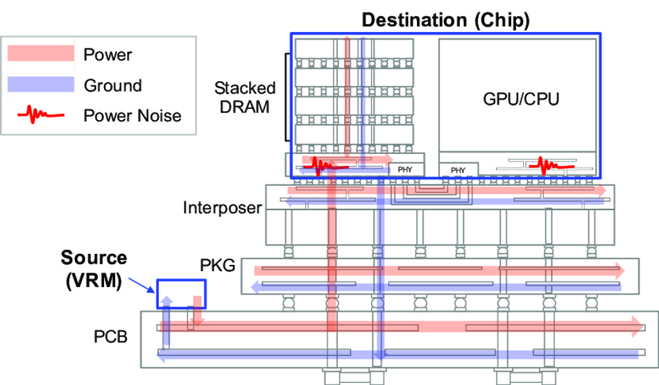
1. Inadequate Power Delivery Network (PDN):
Poorly designed PDNs can lead to voltage droops over 5%, resulting in timing violations.
2. Thermal Bottlenecks:
HBM3 stacks produce heat flux densities above 50 W/cm², and exceeding 105°C junction temperature can cause 20–30% bandwidth throttling.
3. Signal Integrity Failures:
High-speed interfaces can experience bit error rates above 10⁻¹⁵, requiring aggressive ECC to maintain reliability.
4. TSV Yield Issues:
Up to 20–30% of TSV connections can fail due to manufacturing defects without proper redundancy planning.
5. Suboptimal Controller Tuning:
Inaccurate memory timing parameters can reduce performance to 60–70% of theoretical bandwidth.
Verification and Compliance for Robust Implementation
Effective verification strategies are essential. Techniques such as Built-In Self-Test (BIST) patterns stress all memory banks simultaneously to catch timing issues early. Compliance with JEDEC JESD238 standards is also mandatory, ensuring alignment with the electrical and mechanical specifications of HBM3 DRAM.
ECC and Real-Time Error Correction
Modern HBM3 systems include on-die ECC with SECDED (Single Error Correction, Double Error Detection) functionality, safeguarding memory integrity. Additionally, real-time error scrubbing features proactively scan and correct accumulated errors before system-level faults arise—vital for mission-critical workloads and data centre reliability.
Recent Developments Push Boundaries of Memory Technology
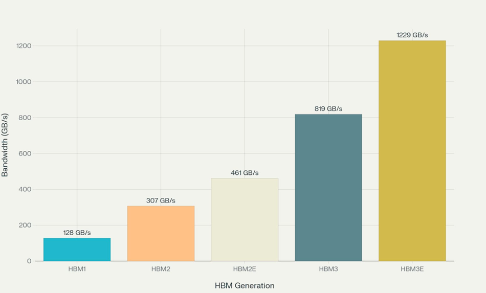
HBM3E Sets New Industry Benchmarks
The HBM3 ecosystem is evolving at an unprecedented pace. With the finalization of HBM3E specifications by JEDEC in May 2023, the next generation of high bandwidth memory now achieves data rates of up to 9.8 Gbps and 1.229 TB/s bandwidth per stack—a dramatic leap in performance. In a major industry milestone, 36 GB HBM3E (2024) by Samsung stands as the highest-capacity implementation to date. This solution employs 12-high 3D-stacked DRAM dies, combined with advanced thermal compression bonding techniques, delivering compact form factors without compromising on heat dissipation or signal integrity.
Manufacturing Breakthroughs Enable Scalability
On the manufacturing front, SK Hynix has reported 80% yield rates for HBM3E production, significantly improving upon initial HBM3 processes. Their use of the Mass Reflow Molded Underfill (MR-MUF) technique facilitates reliable 16-high die stacking, paving the way for HBM4 scalability. This process not only enhances vertical integration but also reduces manufacturing time by 50%, improving production throughput and cost efficiency for large-scale deployments in data centers and AI accelerators.
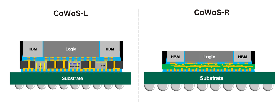
Meanwhile, CoWoS-L Packaging Platform (2024) by TSMC introduces embedded bridge die solutions, supporting larger package areas exceeding 3,800 mm². This design supports up to 12 HBM3 stacks on a single substrate with fine-pitch interconnects, pushing memory capacity and power efficiency to new levels for next-generation HPC and GPU systems.
Emerging Technologies: Optical and 3nm Innovations
The ecosystem is also witnessing exploratory research into photonic integration. Research institutions are testing optical interconnects that pair with HBM3 stacks to potentially replace traditional electrical signaling. Early prototypes demonstrate a 10x reduction in interconnect power consumption while preserving nanosecond-level latencies, offering exciting prospects for future low-power, high-speed AI training systems.
In commercial deployments, Global Unichip Corporation (GUC) has announced the adoption of 3nm HBM3E controller IP by leading cloud service providers. Their controller IP has achieved silicon-validated data rates of 9.2 Gbps on both CoWoS-S and CoWoS-R platforms, marking a critical advancement in HBM3E controller technology for hyperscale and enterprise use.
Advanced Techniques Reveal Sophisticated Optimization Strategies
Adaptive Refresh and Machine Learning-Based Access
To maximize performance, HBM3 systems increasingly employ adaptive refresh management, dynamically adjusting refresh intervals based on temperature profiles and workload patterns. This results in 15–25% refresh overhead reduction, contributing to improved power consumption and sustained data integrity across wide thermal ranges.
Sophisticated memory controllers are now integrating machine learning algorithms for predictive page management. These intelligent page policy mechanisms analyze usage patterns to preemptively open or close memory pages, boosting page hit rates beyond 85%, compared to traditional systems that average only 70%. The resulting gains in memory bandwidth and latency reduction are especially beneficial for real-time AI inference tasks.
Quality-of-Service (QoS) and Real-Time Arbitration
Modern HBM3 memory controllers incorporate Quality-of-Service (QoS) capabilities, enabling traffic prioritization across the 16 independent memory channels. This ensures that latency-sensitive workloads—such as AI model inference—are serviced within sub-microsecond response times. Hardware-based arbitration mechanisms provide guaranteed execution windows, ensuring system determinism even under high bandwidth saturation.
Research-Level Applications: Neuromorphic Architectures
The unique parallel channel structure by HBM3 is also being investigated for neuromorphic computing architectures, where memory bandwidth and structure can simulate the synaptic connectivity found in biological neural networks. These systems leverage high-throughput and low latency to emulate neural behavior with incredible efficiency.
Initial findings show 100x energy savings over traditional von Neumann architectures for certain AI inference tasks, marking HBM3 as a key enabler in the future of machine learning hardware.
Quantitative Performance Metrics Guide Engineering Decisions
Benchmarking Real-World HBM3 Performance
Evaluating HBM3 memory performance goes far beyond theoretical memory bandwidth. Comprehensive benchmarking—including STREAM tests and real-world stress scenarios—reveals a practical ceiling of 3.4 TB/s measured throughput for production HBM3 systems. This represents an impressive 85% bandwidth efficiency compared to the theoretical 4.0 TB/s per multi-stack configuration, reflecting the role of controller tuning, interconnect layout, and memory interface optimization in achieving near-peak performance.
Power and Latency Metrics: Efficiency in Every Bit
Power efficiency is a key design factor, especially for data center and AI training deployments. HBM3 operates at just 2.5 picojoules per bit (pJ/bit)—a 68% improvement over GDDR6X, which consumes 4.2 pJ/bit under equivalent workloads. In latency-sensitive applications, HBM3 achieves an average random-access latency of 120 nanoseconds, outperforming DDR5, which averages 160 nanoseconds under similar memory patterns. These metrics position HBM3 as an ideal memory solution for workloads requiring a combination of low latency, low power, and high-speed throughput.
Cost-Performance and TCO Optimization
In terms of cost-performance, HBM3 shines in use cases where bandwidth densities exceed 500 GB/s. In such cases, alternatives like DDR5 or GDDR6X become inefficient due to either physical footprint or excessive power consumption. A full Total Cost of Ownership (TCO) analysis for data center use shows break-even points at around 70% sustained memory utilization across three-year deployment cycles. These findings support the deployment of HBM3 in AI, HPC, and machine learning environments where long-term operational efficiency is paramount.
Reliability and Data Integrity in HBM3 Systems
Reliability metrics for HBM3 confirm its readiness for enterprise-grade deployments. Mean Time Between Failures (MTBF) exceeds 500,000 hours under typical operating conditions, and the uncorrectable error rate remains below 10⁻¹⁷, thanks to robust on-die ECC and real-time error scrubbing. These values affirm the role of HBM3 in critical systems where memory technology must meet stringent uptime and data retention requirements.
Future Directions Integrate HBM4 and Optical Interconnect Technologies
HBM4: Doubling Down on Performance and Parallelism
The memory roadmap extends confidently toward HBM4, with mass production targeted for 2026. HBM4 will introduce 32-channel architectures using 64-bit channels, doubling parallelism and targeting 1.6 TB/s bandwidth per stack.

This next evolution in 3D-stacked memory architecture will further cement HBM as the dominant high-performance memory format in AI accelerators, HPC systems, and GPU-based architectures.
Optical Interconnects: The Future of Terabit Data Transfer
Emerging technologies like optical interconnects are redefining memory communication paradigms. Silicon photonics offers chip-to-chip communication at terabit-per-second (Tb/s) speeds with a fraction of the power required by traditional electrical signaling. Research prototypes using co-packaged optics with HBM3 stacks have demonstrated up to 100x bandwidth density improvements, positioning optical memory solutions as a foundational element of next-generation computing architectures.
Quantum and Cryogenic Applications
In research settings, HBM3 is also being tested for quantum computing compatibility. Experiments have shown stable HBM3 operation down to 77 Kelvin, made possible through custom refresh algorithms and specialized thermal management. These developments suggest that HBM memory could play a future role in cryogenic environments required by superconducting quantum processors.
Market Outlook and Investment Trends
The global AI accelerator market is projected to grow at a 25% CAGR through 2030, with HBM3 and successor technologies expected to command over 60% market share in high-performance computing domains. Backing this trend, investment in HBM manufacturing capacity has already surpassed $50 billion globally, with major contributions from Samsung, SK Hynix, Micron, and TSMC to expand packaging, stacking, and photonic capabilities through 2027.
Engineering Guidance for 2025 and Beyond
Engineers deploying HBM3-based systems should closely monitor JEDEC standard updates, vendor IP roadmaps, and emerging packaging formats (e.g., FOWLP, CoWoS-L, and embedded bridge dies). Mastery of signal integrity, power delivery optimization, and thermal engineering will be essential for harnessing the full capabilities of HBM3 and transitioning into HBM4, HBM3E, and future optical interconnect-based solutions.
Recommended Reading: Silicon Photonics: A Comprehensive Guide to the Future of Optical Communications
Conclusion
The evolution of High Bandwidth Memory 3 (HBM3) represents a significant leap in memory technology, offering ultimate bandwidth, power efficiency, and scalability for modern computing systems. Its advanced 3D architecture, silicon interposer integration, and controller IP support future-ready designs with enhanced reliability and compact form factors. The industry now transitions toward HBM3E, HBM4, and optical interconnects, so, engineers must stay informed of JEDEC standards, packaging breakthroughs, and design optimization techniques. The future of memory technology lies in architectures that balance speed, density, and energy efficiency, and HBM3 has firmly positioned itself as the foundation of that future. For those designing next-generation systems, it’s essential to build truly scalable, future-ready platforms.
Frequently Asked Questions
Q. What makes HBM3 faster than previous memory generations?
HBM3 achieves superior performance through doubled channel count (16 vs 8), higher data rates (6.4 Gbps vs 3.6 Gbps), and reduced latency via 3D stacking architecture.
Q. How does HBM3 power consumption compare to GDDR6X?
HBM3 consumes approximately 40% less power per bit transferred, utilizing 1.1V core voltage and 0.4V I/O signaling compared to GDDR6X's higher operating voltages.
Q. What applications benefit most from HBM3 implementation?
AI training, large language models, high-performance computing, and real-time ray tracing achieve the greatest performance improvements due to bandwidth-intensive workloads.
Q. Why do HBM3 implementations require silicon interposers?
The 1024-bit interface requires approximately 1,700 signal traces that exceed standard PCB routing capabilities, necessitating fine-pitch silicon interposer technology.
Q. What are the main manufacturing challenges for HBM3?
TSV yield rates, thermal management during assembly, and precise die stacking alignment represent the primary manufacturing obstacles.
Q. How does HBM3 reliability compare to conventional memory?
HBM3 incorporates on-die ECC, real-time error scrubbing, and advanced RAS features, achieving MTBF exceeding 500,000 hours.
References
[1] Rambus Inc. HBM3E: Everything You Need to Know [Cited 2025 June 23] Available at: Link
[2] Wikipedia. High Bandwidth Memory [Cited 2025 June 23] Available at: Link
[3] Supermicro. What Is HBM3? [Cited 2025 June 23] Available at: Link
[4] Tom's Hardware. HBM3 Spec Reaches 819 GBps of Bandwidth and 64GB of Capacity [Cited 2025 June 23] Available at: Link
[5] Electronic Design. What's the Difference Between HBM3 and HBM2E: New Frontrunner [Cited 2025 June 23] Available at: Link
in this article
1. Introduction2. Theoretical Foundations Reveal The Revolutionary 3D Memory Architecture of HBM3Architecture Design Techniques Leverage Advanced 2.5D Packaging Methodologies4. Industry Applications Span from Artificial Intelligence to High-Performance Computing5. Integration with Silicon Interposer Technology Enables Unprecedented Memory Density6. Modern Design Tools Revolutionize HBM3 System Implementation7. Best Practices Address Critical Implementation Challenges8. Recent Developments Push Boundaries of Memory Technology9. Advanced Techniques Reveal Sophisticated Optimization Strategies10. Quantitative Performance Metrics Guide Engineering Decisions11. Future Directions Integrate HBM4 and Optical Interconnect Technologies12. Conclusion13. Frequently Asked Questions14. References