HBM Memory: Complete Engineering Guide & Design Optimization 2025
Master HBM memory technology with our comprehensive engineering guide covering 3D stacking architecture, bandwidth calculations, and design optimization techniques. Discover implementation strategies for AI and HPC applications!

24 Jun, 2025. 14 minutes read
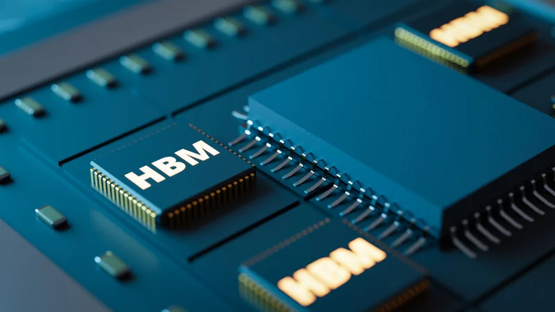
High bandwidth Memory (HBM) Technology
Introduction
HBM Memory (High Bandwidth Memory) has emerged as a critical technology for accelerating data-intensive applications such as AI, machine learning, and graphics processing. Unlike traditional memory architectures, HBM memory offers significantly higher bandwidth, lower power consumption, and compact form factors, making it ideal for modern SoCs and advanced packaging solutions. Engineers and system architects are increasingly turning to HBM memory to meet the growing demand for performance scalability and efficient data throughput.
This comprehensive guide delves into the intricate engineering principles and design optimizations that define contemporary HBM memory architectures. We will explore its unique stacked-die configuration, through-silicon via (TSV) interconnects, and the system-level considerations necessary to harness the full potential of HBM in next-generation computing platforms.
Theoretical Foundations Reveal Revolutionary Bandwidth Architecture of HBM Memory
Unleashing Terabit-Scale Bandwidth with 3D-Stacked DRAM
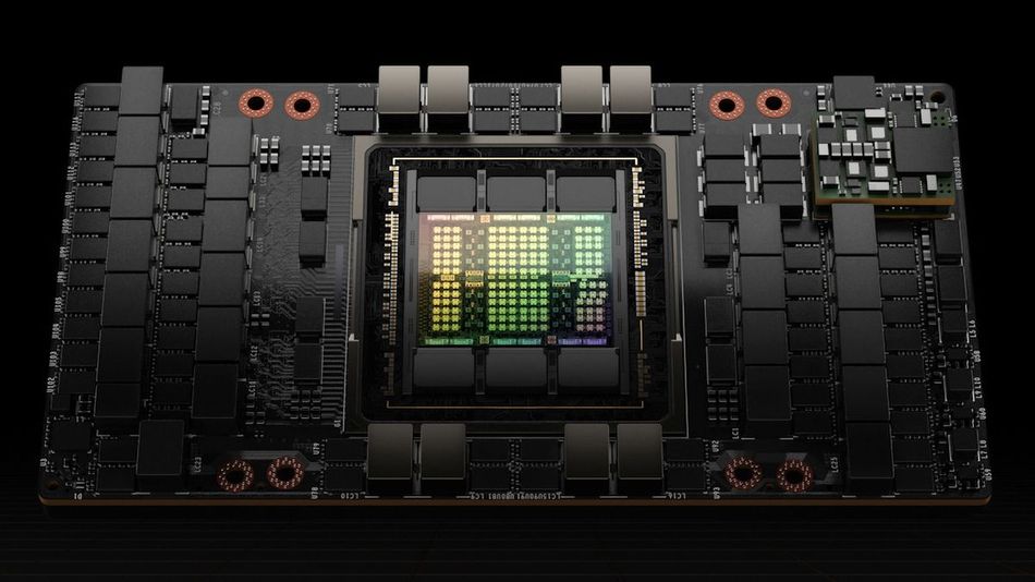
Modern HBM memory architectures achieve unprecedented bandwidth densities, now exceeding 1.2 TB/s, thanks to groundbreaking 3D-stacked DRAM technologies. [1] Unlike traditional DDR and GDDR memory interfaces that rely on high-frequency signaling, High Bandwidth Memory (HBM) employs vertically stacked DRAM dies connected through Through-Silicon Vias (TSVs), delivering wide, parallel data access. These TSVs pass through the entire memory stack, linking each layer directly to the interposer and drastically minimising latency while maximizing data transfer throughput.
With a 1024-bit memory interface, HBM memory achieves 10–30x higher memory bandwidth than legacy DDR5 systems. This architectural shift has made HBM the preferred memory solution for applications in AI training, HPC workloads, supercomputers, and data center accelerators.
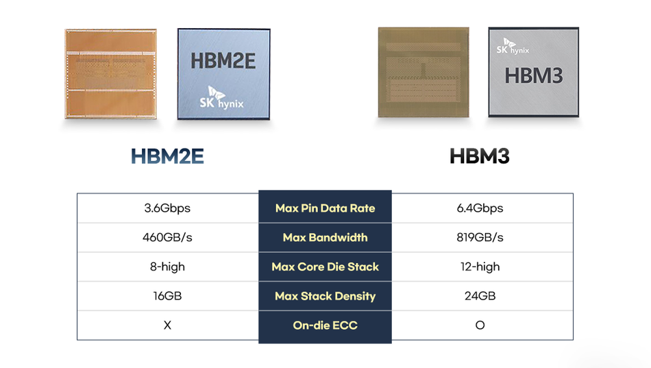
HBM3 and HBM3E: Evolution of Performance and Efficiency
The generational progression from HBM1 to HBM3E memory showcases dramatic improvements. While HBM1 debuted with 128 GB/s in 2013, HBM3E now delivers up to 1,229 GB/s per stack. The efficiency of this design lies in its massive parallelization rather than clock speed. Each HBM stack includes multiple 64-bit channels—typically 8 to 16, which operate concurrently.
For example, using this formula:
Total Bandwidth = (Channels × Channel Width × Data Rate) ÷ 8
HBM3 Example = (16 × 64 bits × 6.4 Gbps) ÷ 8 = 819.2 GB/s
In terms of power efficiency, HBM3 offers up to 141.2 GB/s/W, significantly outperforming conventional DDR modules and even advanced GDDR6 alternatives. These improvements are essential for energy-constrained environments such as edge AI systems and large-scale GPU accelerators.
Recommended Reading: HBM2 vs GDDR6: Engineering Deep Dive into High-Performance Memory Technologies
2.5D Packaging and Silicon Interposer Integration
Effective implementation of HBM memory in 2025 relies on sophisticated 2.5D advanced packaging techniques. [2] These involve mounting the memory and CPU/GPU onto a shared silicon interposer, which provides ultra-high-speed interconnection and signal routing across thousands of traces.
The typical interposer in an HBM3E configuration must support:
Over 1,700 signal traces
Controlled impedance at 50Ω ±10%
Crosstalk isolation through ground plane segmentation
Matched trace lengths within ±5 picoseconds
Support for TB/s-scale throughput
Design Workflow and Optimization Phases
Designing for HBM3 and HBM3E integration involves five critical phases:
Interposer Layout – Define trace topology and minimize reflection loss.
TSV Optimization – Placement must consider die stack height, heat flow, and signal latency.
Power Delivery Network (PDN) – Voltage regulation must maintain clean rails for ~1.2V or lower.
Thermal Management – Heat sinks, microchannels, or integrated vapour chambers manage dissipation across stacked DRAM chips.
Signal Timing & Validation – Simulations must validate operation up to 6.4+ Gbps across 16 channels.
Signal Integrity and Electromagnetic Compliance
Modern HBM memory implementations reach more than 95% signal integrity by leveraging advanced electromagnetic simulation tools. Engineers must manage:
Via inductance under 100 pH
Controlled TSV impedance
Ground reference stitching to prevent loop currents
Noise shielding between lanes
Active power-plane decoupling for reduced ripple and enhanced power consumption balance
These engineering best practices ensure reliable data transfer at high transfer rates, especially critical for AI workloads, semiconductor SoCs, and HBM3E-based NVIDIA, AMD, or Intel platforms.
Applications of HBM Memory: From AI Training to Supercomputing Excellence
Revolutionizing AI Training with Massive Bandwidth
HBM memory plays a pivotal role in artificial intelligence training, enabling accelerated model development and inference at scales previously unattainable with conventional DDR or GDDR memory. Industry-leading platforms like H100 GPU by NVIDIA, equipped with HBM3E memory, achieve aggregate memory bandwidth of up to 3.35 TB/s, supporting real-time training of large language models with over 100 billion parameters. [3]
Currently, in 2025, AI workloads represent the largest market share for HBM deployment, with HBM3E becoming the memory of choice for systems requiring ultra-fast data transfer, low latency, and tight energy budgets. AI model developers benefit from 2–5x throughput increases while consuming less power compared to DDR5 or GDDR6-based systems.
HBM in Graphics Processing and Visualization
For graphics cards and professional rendering applications, the high-speed, low-latency architecture of HBM2E and HBM3 provides notable performance gains. Systems utilizing HBM-equipped GPUs deliver over 60 FPS in 4K gaming environments and demonstrate 40% faster rendering for 3D models in professional visualization software compared to GDDR-based architectures.
The wide memory interface of HBM stacks, combined with parallel channel access, eliminates bottlenecks during high-speed graphics processing. This makes HBM memory ideal for VR rendering, real-time ray tracing, and motion graphics pipelines.
Empowering High-Performance Computing (HPC) and Scientific Simulations
In high-performance computing (HPC) environments, HBM memory has transformed the way scientists and engineers approach simulation-heavy workloads. Applications such as computational fluid dynamics, weather modeling, and molecular dynamics report 2–4x performance improvements using HBM3 accelerators.
Moreover, power efficiency by HBM—exceeding 180 GB/s per watt—has become a crucial advantage in reducing overall system energy use by 15–25%, especially in multi-node HPC clusters. This efficiency translates into cost-effective scalability and higher performance-per-watt for government labs, academic institutions, and industrial research centers.
HBM3E in Data Center Deployments
Leading data center operators are rapidly adopting HBM3E in AI-optimized servers and accelerators. The migration from DDR4 to HBM3E results in a reduction of up to 30% in memory-related power consumption, significantly cutting operational expenses in hyperscale environments.
Additionally, HBM memory simplifies form factor constraints by vertically stacking dies, allowing for higher memory capacity in a smaller footprint. This is particularly beneficial for dense server racks and modular data center designs that require compact, high-efficiency solutions.
The High-Bandwidth Memory Chip Market is projected to grow at an annual rate of 42% between now and 2033, reaching around $130 billion, according to a report by Bloomberg Intelligence.
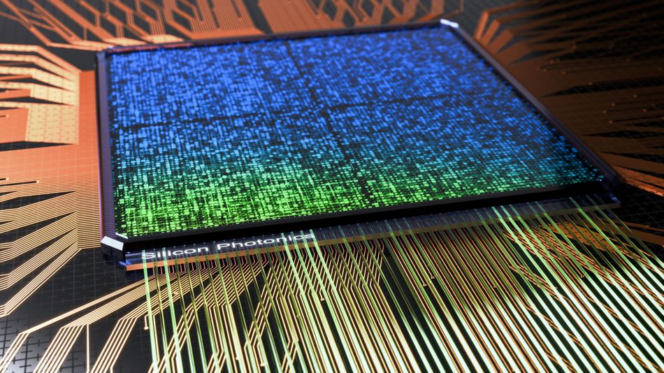
Next-Gen Integration: Silicon Photonics & Hybrid Bonding
A groundbreaking evolution in HBM integration is its pairing with silicon photonics, enabling aggregate throughput exceeding 10 TB/s. These photonic interconnects overcome traditional electrical limitations and support distributed AI training at massive scales, while preserving the low-latency characteristics of HBM.
In 2025, hybrid bonding techniques are becoming a viable alternative to interposer-based designs. This enables direct die-to-die connections between the HBM stack and the host processor, eliminating interposer-induced signal integrity issues and supporting 10-micron pitch connections.
Thermal & Power Co-Design Strategies
Managing thermal and power delivery is a critical design priority for HBM3E implementations. Each HBM stack can generate over 20 watts of thermal load, requiring advanced thermal interface materials (TIMs) with a conductivity greater than 5 W/mK. Maintaining junction temperatures below 85°C is vital to avoid thermal throttling or performance degradation.
Engineers must also ensure:
Power delivery ripple below 2%
Robust PDN (Power Delivery Network) design
EMC (Electromagnetic Compatibility) shielding
Optimized signal timing validation across all memory channels
Failure to address these factors results in unstable operation and a degraded functional bandwidth.
Recommended Reading: Silicon Photonics: A Comprehensive Guide to the Future of Optical Communications
Modern Design Tools Revolutionize HBM Memory Implementation Workflows
EDA Tools Tailored for High Bandwidth Memory Design
As HBM memory technologies evolve, Electronic Design Automation (EDA) tools have become indispensable for managing the complexity of 3D-stacked architectures, interposer routing, and multi-gigabit signal paths.

Next-generation design platforms now offer purpose-built solutions for HBM3E and beyond, enabling faster design cycles, higher reliability, and robust signal integrity assurance.
Key HBM Design Tools and Capabilities
| Tool | Developer | Core Focus | Performance Metric |
| Virtuoso | Cadence | PHY Design | 12.4 Gbps Support |
| DesignWare | Synopsys | Controller IP | 95% First Pass Success |
| Xpedition | Siemens | 2.5D Interposer | ±1% Signal Length Matching |
| Rambus IP | Rambus | HBM3E Controller | 10.4 Gbps + ECC + BIST |
Cadence Virtuoso: PHY-Level Design Optimization
Cadence Virtuoso offers a complete PHY design solution for HBM3E memory systems, supporting speeds up to 12.4 Gbps. [4] The tool integrates signal integrity analysis, electromagnetic (EM) simulation, and automated layout optimisation into a single, cohesive environment. Engineers can rapidly prototype memory interfaces while maintaining compliance with TSV routing and interposer design constraints.
Synopsys DesignWare: Controller-Level Integration
The DesignWare HBM Controller IP by Synopsys facilitates end-to-end HBM memory controller implementation, offering built-in training algorithms, adaptive timing calibration, and power-aware interface tuning. This results in a 95% first-pass success rate, significantly reducing the number of design iterations and expediting production-level deployments in data centers, AI accelerators, and HPC systems.
Siemens Xpedition: Interposer and 2.5D Packaging Mastery
Siemens Xpedition Package Designer is optimized for 2.5D packaging workflows, supporting automated via fanout generation, comprehensive HBM channel routing, ±1% trace length matching tolerance, and over 1,000 signals routed per design. These capabilities are critical for maintaining low latency, matched timing, and minimal crosstalk in high-density HBM stack interconnects.
Rambus HBM3E Controller: Adaptive Performance Across Conditions
The Rambus HBM3E Controller sets the bar with 10.4 Gbps operational bandwidth, supported by Built-in Self-Test (BIST) and Error Correction Code (ECC). Adaptive tuning algorithms dynamically calibrate parameters across process, voltage, and temperature fluctuations (PVT variations). Such features make it highly reliable for mission-critical AI training, graphics, and scientific workloads where consistent memory bandwidth is essential.
Quantified Gains with Modern Design Platforms
According to performance benchmarks from leading EDA vendors. Design closure time has improved by 2–3x over legacy memory workflows. Manual tuning effort is reduced by up to 70% through automation. Enhanced power efficiency and signal timing accuracy ensure stable operation at terabit-per-second (Tb/s) scale bandwidths.
As HBM memory integration complexity increases with HBM3E, HBM4, and beyond, these specialized design platforms ensure scalable, reliable, and efficient implementation across industries.
Best Practices Address Thermal Management and Signal Integrity Challenges
Thermal Management: The Cornerstone of Reliable HBM Systems
Modern HBM memory stacks, especially HBM3E configurations, operate with dense die stacking and ultra-high throughput, generating significant heat during intensive workloads. Maintaining junction temperatures below 85°C is critical to prevent thermal throttling, signal degradation, and long-term reliability issues.
Engineers employ multi-layer thermal design strategies, including:
Advanced thermal interface materials (TIMs) with >5 W/mK conductivity
Heat spreaders coupled with direct-to-chip cooling
Active airflow pathways within compact 2.5D packaging environments
Integration with system-level cooling architectures for sustained high-performance operation
These thermal co-design strategies are essential, particularly in AI training, HPC, and data center applications where thermal load exceeds 20W per stack.
Ensuring Signal Integrity at Terabit Scales
With over 1,024 signals in typical HBM3E systems, signal integrity becomes a mission-critical concern. Verification involves comprehensive simulation and measurement across high-speed channels, with focus areas including:
S-parameter extraction for impedance and reflection analysis
Eye diagram analysis at 6.4–9.8 Gbps to visualize voltage/time margin
Jitter budgeting for validating timing skew across multiple stacks
Power supply noise evaluation and ripple containment
EMI compliance testing to avoid cross-domain interference
These steps ensure consistent high-speed communication across stacked TSV-connected dies and the interposer network.
PDN Design: Meeting High Instantaneous Current Demand
The power delivery network (PDN) must support dynamic current demands up to 50A, especially during AI accelerations and memory bursts. Best practices include:
Maintaining voltage levels within ±3% regulation across all stacks
Strategic decoupling capacitor placement to minimize parasitic inductance
Using multi-phase VRMs with fine-grain dynamic response
Ensuring low power plane impedance throughout the memory stack interface
Well-designed PDNs reduce voltage droop and mitigate performance instability during peak throughput operations.
Yield Optimization and Reliability Validation
To ensure high-volume production of HBM memory, manufacturers apply Design for Test (DFT) principles:
IEEE 1500-compliant internal test interfaces for access to embedded DRAM arrays
Built-in self-test (BIST) features for early-stage fault detection
Redundant via paths and ECC (Error Correction Code) integration
Leading foundries report >95% production yields in complex HBM3E packages when these protocols are followed.
Long-term reliability testing includes:
Accelerated aging at elevated temperatures
Electromigration stress testing on TSVs
Thermal cycling over 100,000+ solder joint cycles
These tests validate the structural and electrical robustness of HBM stacks under extreme usage scenarios.
Recent Developments Push the Boundaries of HBM Architecture
HBM3E Launch and Industry Leadership
Launched in 2024, HBM3E memory delivers 9.8 Gbps per pin while remaining backward compatible with HBM3 controllers. SK Hynix leads mass production with 12-high die stacks capable of 1.2+ TB/s bandwidth, consolidating industry leadership in AI accelerator memory solutions.
HBM4 and the Shift to Interposer-Free Architectures
Samsung is driving innovation with HBM4 development on its 4nm process node, targeting mass production in 2026. [5] The revolutionary interposer-free packaging approach significantly lowers system complexity and manufacturing costs by 20–30% while preserving high-speed operation. This advancement could reshape semiconductor economics in next-generation memory technologies.
Looking Ahead: HBM5 and In-Memory AI Processing
3D System-in-Package (SiP) concepts are currently in research stages, aiming to integrate HBM5 with near-memory compute capabilities. This in-memory processing architecture can reduce AI inference energy consumption by 5–10 times for dedicated tasks, such as transformer model execution or video recognition.
Silicon Photonics: The Path to 100x AI Scaling
Silicon photonic integration is poised to revolutionize AI systems by enabling multi-terabit interconnects between HBM memory modules and AI accelerators. Early tests from global foundries indicate that this approach may enable 100x scalability over current memory bus limits, overcoming bandwidth bottlenecks while preserving low latency and compact form factors.
Recommended Reading: System in Package: A Comprehensive Guide to SiP Technology
Advanced Techniques Reveal Sophisticated AI Training Optimisations
Optimizing HBM Memory Bandwidth for AI Workloads
Training large-scale AI models—especially transformer-based architectures with 100B+ parameters—requires memory systems that deliver high throughput with minimal overhead. Cutting-edge batch size scaling algorithms now maximize HBM memory utilization by aligning data loads with stack-level access granularity. These advanced batching techniques reach >90% bandwidth utilization, a sharp increase over the sub-60% efficiency of traditional batching workflows.
To enhance throughput, engineers apply multi-stack coordination algorithms that enable coherent access across 4–8 HBM stacks, unlocking aggregate bandwidth exceeding 5 TB/s. By optimizing memory mapping and intelligently distributing data across stacks, inter-stack communication latency is reduced by up to 40%, improving model convergence speed in distributed AI training pipelines.
Dynamic Power Management and Predictive Reliability
Adaptive power management technologies dynamically regulate HBM3E stack frequency and voltage based on real-time thermal conditions and workload types. These systems deliver 15% energy savings while maintaining full performance, crucial for large-scale data center training jobs with sustained loads.
On the reliability front, modern HBM systems integrate advanced ECC algorithms capable of multi-bit error correction and live repair mechanisms to maintain system uptime. Machine Learning-based predictive failure analysis detects early signs of memory cell degradation 24–48 hours before a critical fault occurs, extending overall system resilience and minimizing downtime.
Quantitative Metrics Guide Architectural Choices
To make informed design decisions, engineers must consider a range of quantitative performance metrics:
Bandwidth Efficiency:
HBM3E: 180.7 GB/s per watt
GDDR6X: 40.3 GB/s per watt
Total Cost of Ownership (TCO):
HBM-based AI systems show 25–35% lower operational costs over 3 years, offsetting higher upfront hardware pricing.
Memory Latency:
HBM3E: 190–220 ns
DDR5: 280–320 ns
Critical for real-time inference and low-latency AI applications
Queue Depth Optimization:
Best performance achieved at 16–32 outstanding requests per channel, ensuring pipeline saturation
Scaling Efficiency:
Linear bandwidth scaling up to 8 HBM stacks with <5% coordination overhead
Performance per Dollar:
HBM3E reaches cost parity with GDDR6X at >70% utilization in cloud AI systems
Reliability Benchmarks:
<10 FIT (Failures in Time)
MTBF (Mean Time Between Failures) exceeds 1 million hours, surpassing enterprise DRAM standards
Future Directions: From HBM4 to Compute-in-Memory Systems
HBM4: Redefining Bandwidth and Density Standards
Slated for 2026, the HBM4 standard introduces:
2048-bit interface width
1.6+ TB/s per stack
Up to 64GB per stack with 16-Hi stacking
60% improved power efficiency over HBM2, HBM2E
These advancements align with AI model scaling forecasts for 2027–2028, particularly in foundation model training and edge inference environments.
Monolithic 3D DRAM and In-Memory AI Processing
Research into monolithic 3D Dynamic Random Access Memory (DRAM) shifts memory stacking from die-to-die to true 3D cell architectures, offering:
10x density improvement
Elimination of TSV bottlenecks
Commercial viability projected between 2028 and 2030
Simultaneously, Compute-in-Memory (CIM) technology is being prototyped within HBM stacks, enabling localized neural computation and reducing data movement by 100x. Hybrid solutions combining traditional DRAM with CIM blocks will provide flexible scaling for AI inference tasks such as NLP, vision, and autonomous systems.
Silicon Photonics: Optical Memory Interfaces on the Horizon
Emerging silicon photonic co-packaging solutions aim to deliver optical memory interfaces with bandwidths exceeding 100 TB/s between memory modules and compute cores. Wavelength Division Multiplexing (WDM) techniques allow multiple parallel optical channels within a single fiber, overcoming current electrical interconnect limitations.
These advancements promise ultra-low latency, reduced electromagnetic interference, and unprecedented scalability for next-generation AI architectures.
Strategic Considerations for AI Hardware Teams
Engineering leaders planning systems beyond 2026 must align HBM memory roadmaps with emerging photonic, monolithic, and in-memory compute technologies. The choice of memory architecture will significantly influence system scalability, cost, efficiency, and reliability.
Recommended Reading: The 2025 Edge AI Technology Report
Conclusion
As AI, HPC, and data center workloads push the boundaries of performance, HBM memory has emerged as the cornerstone of next-generation computing systems. Through innovations in 3D stacking, interposer design, adaptive power management, and advanced error correction, HBM3E and future HBM4 architectures deliver unmatched bandwidth, energy efficiency, and reliability. From optimized AI training pipelines to silicon photonic integration, this guide has explored the critical techniques engineers must adopt for effective HBM deployment in 2025 and beyond. Mastering HBM memory design is no longer optional—it’s essential for building scalable, future-ready systems that lead in performance and innovation.
Frequently Asked Questions
Q. What is the main difference between HBM and DDR memory architectures?
A. HBM uses 3D-stacked DRAM dies with 1024-bit wide interfaces connected via silicon interposers, while DDR memory uses planar chips with 64-bit interfaces on PCBs. This architectural difference enables HBM to achieve 10-30x higher bandwidth density.
Q. What are the primary thermal design challenges with HBM implementation?
A. HBM stacks generate 15-25W in compact form factors, requiring specialized thermal solutions to maintain junction temperatures below 85°C. Advanced thermal interface materials and heat spreader design are essential.
Q. Which applications benefit most from HBM memory technology?
A. AI training workloads, high-performance computing simulations, professional graphics rendering, and real-time data analytics show 2-10x performance improvements with HBM implementations. Memory-bandwidth-limited applications see the greatest benefits.
Q. What is the cost difference between HBM and traditional memory solutions?
A. HBM costs approximately 5x more per GB than DDR5 and 3x more than GDDR6, but provides superior performance-per-watt and enables system-level cost reductions in high-performance applications. TCO analysis shows break-even at >70% utilization rates.
Q. How does HBM4 differ from current HBM3E technology?
A. HBM4 doubles interface width to 2048 bits, increases capacity to 64GB per stack, and targets 60% power efficiency improvement while maintaining backwards compatibility with HBM3 controllers.
References
[1] GlobeNewsWire. Memory and Storage Technology Research Report 2025 [Cited 2025 June 16] Available at: Link
[2] EdgeAIVision. Advanced Packaging: How AI is Revolutionizing the Game [Cited 2025 June 16] Available at: Link
[3] NVIDIA. H100 Tensor Core GPU [Cited 2025 June 16] Available at: Link
[4] Business Wire. Cadence Enables Next-Gen AI and HPC Systems with Industry’s Fastest HBM4 12.8Gbps IP Memory System Solution [Cited 2025 June 16] Available at: Link
[5] KED Global. Samsung to Mass Produce HBM4 on 4 nm Foundry Process [Cited 2025 June 16] Available at: Link
in this article
1. Introduction2. Theoretical Foundations Reveal Revolutionary Bandwidth Architecture of HBM Memory3. Applications of HBM Memory: From AI Training to Supercomputing Excellence4. Modern Design Tools Revolutionize HBM Memory Implementation Workflows5. Best Practices Address Thermal Management and Signal Integrity Challenges6. Recent Developments Push the Boundaries of HBM Architecture7. Advanced Techniques Reveal Sophisticated AI Training Optimisations8. Future Directions: From HBM4 to Compute-in-Memory Systems9. Conclusion10. Frequently Asked Questions11. References