Ball Grid Array Technology: Complete Engineering Guide
Ball Grid Array (BGA) is a high-density packaging technology using solder balls for connections. This guide covers BGA design principles, performance advantages, modern applications (2000+ pins in 45mm), and cutting-edge implementation techniques for engineers.

15 Jun, 2025. 15 minutes read
Introduction
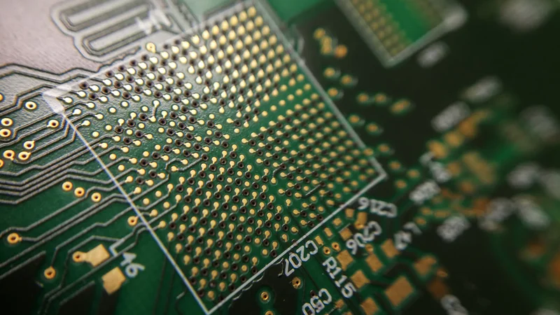
Ball Grid Array (BGA) packaging has become the gold standard for high-density integrated circuits in modern electronics, where performance and miniaturization are critical. By replacing traditional perimeter leads with an array of microscopic solder balls, BGA technology enables unparalleled connection density, superior signal integrity, and enhanced thermal performance compared to conventional packaging methods.
Today's cutting-edge BGA packages achieve pin counts exceeding 2,000 in compact footprints under 45mm². At the same time, advanced variants like wafer-level and ceramic BGAs push the boundaries of what's possible in high-frequency and harsh-environment applications. From smartphones to spacecraft, this revolutionary packaging approach enables breakthroughs across industries by solving fundamental challenges in power delivery, heat dissipation, and signal routing at ever-shrinking scales.
The unique self-aligning nature of BGA solder balls during reflow, combined with their shorter electrical paths, makes them particularly valuable for high-speed digital systems, RF designs, and power electronics. However, realizing these benefits requires careful consideration of material properties, thermal management strategies, and manufacturing processes. While BGAs offer superior density, their successful implementation demands rigorous Design for Manufacturability (DFM) considerations from the outset, ensuring that these theoretical advantages translate into reliable and cost-efficient production.
The Physics Behind BGA's Superior Performance
The structural advantages of BGA packaging become evident when examining its underlying mechanics. The grid arrangement of solder balls creates a robust mechanical connection through uniform stress distribution during thermal cycling, significantly improving long-term reliability compared to leaded packages. This distributed contact system also provides superior current-carrying capacity, with typical BGA interconnects handling 30-50% more current per connection than equivalent peripheral leads.
Thermal and Electrical Advantages
Heat Dissipation: The solder ball array acts as a thermal conduction path, with thermal resistance values typically 40-60% lower than quad flat packages (QFP) packages of comparable size.
Signal Integrity: The shortened connection paths (averaging 0.8-1.2mm) reduce parasitic inductance by 70-80% compared to the perimeter-lead alternative.
Power Delivery: Distributed power/ground balls enable lower impedance power distribution networks, crucial for modern processors
Recommended reading: QFN Packages: A Guide to High-Performance Electronics Encapsulation
Manufacturing Precision
The C4 attachment process achieves remarkable consistency, with modern placement systems achieving:
- Solder ball coplanarity within 25μm
- Joint formation repeatability of ±7μm
- Self-alignment accuracy exceeding 97% for pitches down to 0.3mm
These characteristics make BGA technology particularly valuable for applications demanding high reliability and electrical performance, from automotive control modules to high-frequency communication systems. The technology continues to evolve, with new solder alloys and substrate materials pushing the boundaries of interconnection density and thermal performance.
Recommended reading: LGA vs BGA: How to Select the Best IC Package for Your Design
Advanced BGA Routing Methodologies for High-Density Designs
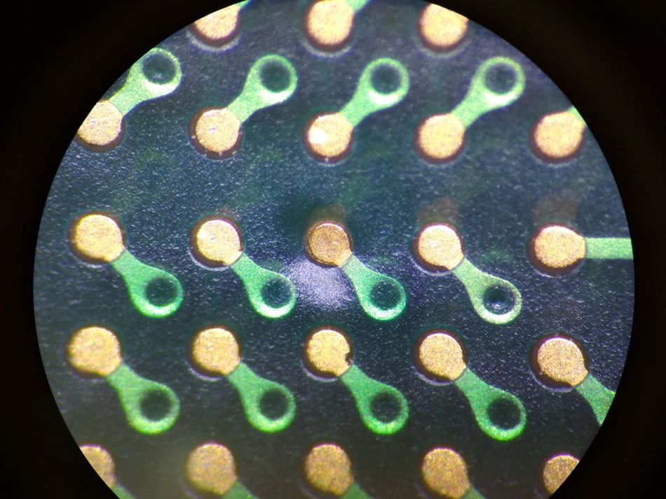
Modern BGA packaging demands innovative PCB routing solutions to maintain signal integrity while optimizing board space. Two primary techniques have emerged as industry standards for different pitch requirements:
1. Dog-Bone Fanout (≥0.8mm Pitch)
Enables efficient escape routing with two signal traces between adjacent balls
Layer count optimization formula:
*Layers Required = (Total Rows - 2) / 2*Example: A 23×23 BGA (529 balls) typically requires 11 signal layers
Benefits: Cost-effective for medium-density designs with 0.8-1.0mm pitch
2. Via-in-Pad Technology (≤0.5mm Pitch)
Critical Implementation Requirements:
Via Dimensions: Max 200µm diameter (0.5mm pitch)
Aspect Ratio: 12:1 maximum for consistent plating
Fill Material: Non-conductive epoxy (≤5µm surface variation)
Surface Finish: 25µm copper cap minimum
Manufacturing Considerations:
Mandates IPC 4761 Type VII processing
Prevents solder wicking during reflow
Enables direct component placement over vias
Thermal Management Solutions
For power BGAs, thermal vias must meet strict performance criteria:
Thermal Resistance (θ) = t / (k × A)
Where:
t = substrate thickness (mm)
k = thermal conductivity (W/m·K)
A = via copper area (mm²)
Design Target: θ ≤ 2°C/W for effective heat dissipation
Implementation Guidelines:
Use arrayed thermal vias under high-power components
Maintain consistent via fill quality
Consider copper plugging for improved thermal transfer
These advanced techniques enable designers to overcome the challenges of modern high-pin-count BGAs while meeting demanding electrical and thermal performance requirements. The choice between methodologies depends on pitch requirements, cost constraints, and manufacturing capabilities. Also, these routing techniques are not merely design choices but core Design for Manufacturability (DFM) strategies, aiming to minimize PCB layer count, reduce signal integrity issues, and ensure robust solder joint formation during mass production.
Recommended reading: Via in Pad PCB Design
High-Performance Applications of BGA Technology: From Automotive to Aerospace and Beyond
Ball Grid Array (BGA) packaging plays a foundational role in high-reliability, high-performance electronics. Its mechanical resilience, electrical efficiency, and thermal performance make it indispensable across sectors like automotive, aerospace, telecommunications, and defense.
In 2024, the global BGA market reached an estimated $8.64 billion, with projections forecasting a 6.0% compound annual growth rate (CAGR) through 2034. This growth is driven by the accelerating demand for advanced, miniaturized electronics in mission-critical applications.
1. Automotive Electronics: Powering the Intelligent Vehicle Revolution
Modern vehicles now contain more than 50 electronic control units (ECUs), many of which utilize BGA packaging for their ability to support complex processing and reliable performance in harsh environments.
Operating Requirements
Temperature range: –40°C to +150°C
Long-term durability: <1 FIT (Failure in Time) over a 15-year lifecycle
Reliability benchmark: 99.97% performance over 200,000 km
Key Automotive Applications
Engine Management Systems: Use flip-chip BGA (FCBGA) packages with 500+ I/O pins. Enable real-time sensor fusion for optimized combustion, emissions, and diagnostics
Infotainment Processors: High-density BGAs handle 4K video at 60 fps, 3D rendering, and AI-driven UI systems
Safety Controllers: Redundant BGA-based architecture compliant with ASIL-D safety standards under ISO 26262
2. Aerospace and Defense: Ruggedized Reliability in Extreme Conditions
Aerospace systems impose some of the harshest requirements on electronic packaging. BGA variants like Ceramic BGA (CBGA) and Plastic BGA (PBGA) are widely adopted for their stability across extreme conditions.
Environmental Requirements
Operating temperatures: –55°C to +125°C
Mechanical durability: 10G shock resistance
Longevity: 500+ thermal cycles with no performance degradation (NASA-tested)
Critical Aerospace Applications
Flight Control Computers: Utilize radiation-hardened BGAs capable of surviving 100 krad total ionizing dose (TID)
Satellite Communications: Hermetically sealed BGA packages ensure stability in Ka-band (26.5–40 GHz) systems
Radar and RF Systems: Use GaN-based BGAs operating up to 40 GHz, enabling high-resolution, long-range detection.
3. Telecommunications Infrastructure: Enabling Ultra-Fast, High-Frequency Networks
The global rollout of 5G and the move toward 6G networks demand packaging technologies that can handle massive bandwidths and operate at extremely high frequencies.
Electrical Requirements
Frequency support: Up to 300 GHz (millimeter-wave) operation
Signal integrity targets:
Dielectric constant (Dk): ≤3.5
Loss tangent (Df): ≤0.003
Integration: Support for optical-electrical hybrid systems
Key Telecom Applications
Base Station Processors: Employ 2000+ pin BGAs to manage 20 Gbps data throughput per lane
Network Switches: Utilize low-latency BGAs achieving <100 ns packet processing for real-time data routing
Fiber Optic Transceivers: Use integrated photonic BGAs supporting 400 Gbps Ethernet and optical interconnects.
Market Impact
Telecommunications accounts for approximately 35% of total BGA demand.
Estimated 2024 sector value: $3.02 billion.
Integration with advanced substrate technologies enables miniaturization
Ball Grid Array (BGA) packages are evolving rapidly to support next-generation electronic systems, integrating seamlessly with advanced substrate technologies. Innovations such as Package-on-Package (PoP) and System-in-Package (SiP) configurations enable significant space and performance optimization, achieving up to 60% footprint reduction without sacrificing electrical integrity.
At the forefront of this evolution is Embedded Wafer-Level Packaging (eWLP), which incorporates active die directly within the substrate layers. By eliminating wire bonds, eWLP reduces overall package height to ≤0.5 mm while supporting high-density interconnects exceeding 400 I/O terminals.
Key Technical Benefits of eWLP:
Parasitic Reduction: Up to 80% lower inductance compared to traditional wire-bonded packages, as well as improved signal integrity for high-speed designs.
Thermal Performance: Up to 3× more efficient heat dissipation via direct thermal paths through the substrate
Cost Efficiency: Enables 25% reduction in manufacturing costs at high production volumes due to streamlined assembly and fewer interconnect layers.
Flexible Integration for Wearables and Medical Electronics
BGA (Ball Grid Array) packages are increasingly being adapted for flexible electronics, unlocking new possibilities in ultra-thin, lightweight, and body-conforming devices for next-generation applications. These include wearable health monitors, implantable biosensors, smart textiles, and epidermal electronics, where space constraints and mechanical compliance are critical. Flexible BGAs use polyimide- or LCP-based substrates that can endure bending radii as tight as 5 mm without mechanical fatigue or electrical discontinuity, thanks to strain-relieved interconnect structures and compliant solder joints.
To ensure long-term reliability, one of the most crucial design parameters is the coefficient of thermal expansion (CTE) matching between the die and the flexible substrate—ideally within ±2 ppm/°C—to minimize thermomechanical stress during cyclic heating and cooling, which could otherwise lead to delamination, solder fatigue, or interfacial cracking. In addition, low-modulus encapsulants and ultra-thin underfills are often employed to accommodate mechanical deformation while maintaining insulation and moisture resistance. These advancements make flexible BGA packaging a cornerstone for miniaturized, rugged, and high-performance bio-integrated systems in emerging healthcare and wearable technologies.
Overcoming Integration Challenges
While the benefits of BGA integration are significant, ranging from miniaturization to enhanced electrical and thermal performance, there are critical challenges associated with high-density packaging, especially during assembly and reflow processes. One major issue is substrate warpage, which can lead to misalignment or solder joint defects. This is typically mitigated through symmetrical stackup designs that balance mechanical stresses across layers and the use of controlled reflow temperature profiles with ramp rates limited to ≤3°C/s to reduce thermal shock.
Another key concern is thermal stress management during operation and cycling. To address this, manufacturers employ advanced underfill materials with a modulus of ≤1 GPa, which effectively absorb mechanical strain between the die and substrate. These materials not only improve mechanical durability but also maintain electrical insulation exceeding 10¹⁰ ohm-cm, ensuring signal integrity and long-term reliability even in harsh environments. Together, these engineering approaches are essential for achieving dependable performance in high-density BGA assemblies used in mission-critical applications.
Modern software tools revolutionize ball grid array implementation
The implementation of Ball Grid Array (BGA) designs has been dramatically transformed by modern PCB design software, which leverages automation, AI-driven optimization, and real-time analysis. In 2025, leading electronic design automation (EDA) tools such as Altium Designer, Cadence Allegro, and KiCad are enabling engineers to reduce BGA routing time by up to 70%, while simultaneously enhancing signal integrity and manufacturability.
Altium Designer 2024: AI-Driven BGA Optimization
Altium Designer's latest release introduces intelligent auto-fanout capabilities specifically tailored for high-pin-count BGA devices. Its constraint-driven routing engine automatically determines optimal via placements, reducing manual effort and minimizing electromagnetic interference (EMI). Key advanced features include:
AI-Based Layer Assignment: Dynamically allocates signal layers to reduce crosstalk and optimize trace lengths.
Real-Time Impedance Calculation: Maintains ±2% impedance tolerance, essential for high-speed signal integrity.
3D Collision Detection: Prevents component interference during placement through real-time spatial analysis.
Thermal Simulation Integration: Enables live junction temperature monitoring for thermal-aware layout planning.
Cadence Allegro: Enterprise-Class BGA Design Suite
Cadence Allegro remains the gold standard for complex BGA and HDI (High-Density Interconnect) PCB designs, particularly in automotive, aerospace, and telecommunications sectors. Supporting packages with over 3000 pins, Allegro provides unmatched scalability and precision. Notable capabilities include:
Constraint-Driven Fanout: Automatically generates BGA escape routing in compliance with IPC-2221/2222 standards
HDI and Microvia Design Rules: Fully supports 0.4 mm pitch BGAs with advanced via-in-pad rules and stacked microvias.
Manufacturing DFM Checks: Real-time IPC-6012 Class 3 verification ensures manufacturability and reliability.
Integrated Signal Integrity Simulation: Leverages IBIS model integration for accurate pre-layout timing and SI validation.
KiCad: Open-Source Alternative with Core BGA Support
KiCad continues to gain popularity among startups, educators, and hobbyists, offering a robust open-source platform for moderate BGA complexity:
Up to 500-pin BGA support with semi-automated routing tools
Basic signal integrity checks and via escape strategies
Zero cost, making it accessible for prototyping and low-volume designs
Performance Comparison Matrix
Tool | Max BGA Pins | Routing Speed | SI Analysis | Cost (2024) |
Altium Designer | 1500 | High | Advanced | $7,500/year |
Cadence Allegro | 3000+ | Highest | Expert | $25,000/year |
KiCad | 500 | Medium | Basic | Free |
Mentor Graphics | 2000 | High | Advanced | $15,000/year |
Best Practices for Reliable BGA Implementation
Achieving a >99.5% first-pass yield in Ball Grid Array (BGA) assembly requires meticulous adherence to design, process, and inspection standards. Common pitfalls such as solder joint defects, package warpage, and invisible interconnect failures can be mitigated through industry-proven best practices.
Solder Joint Integrity
One of the most prevalent issues in BGA assembly is void formation, which affects up to 15–20% of joints when process controls are inadequate. Voids exceeding 25% of the solder ball volume drastically compromise mechanical and thermal performance. To minimize this risk:
Nitrogen Reflow Atmosphere: Reduces oxidation-induced voiding by up to 80%, improving wetting and joint uniformity.
Optimized Solder Paste: Use Type 4 or Type 5 particle sizes for fine-pitch BGAs (<0.5 mm) to ensure consistent stencil printing and reflow behavior.
Controlled Reflow Profiles: Maintain peak temperatures of 245°C ± 5°C for SAC305 alloys to ensure complete reflow and minimize solder voids.
Substrate Preheating: Target a minimum preheat of 120°C to mitigate thermal shock and improve solder joint morphology.
Warpage Control and Stress Management
Excessive package warpage, particularly beyond 100µm, accounts for connection failures in over half of defective BGA assemblies. Preventative design and process measures include:
Balanced Stackup Design: Symmetrical copper layer distribution across the PCB minimizes coefficient of thermal expansion (CTE) mismatch, reducing mechanical stress.
Low-Modulus Underfill Materials: Select underfill compounds with a modulus below 1 GPa at operating temperature to absorb thermal expansion without cracking or delamination.
Optimized Reflow Ramp Rates: Implement ramp-up rates below 3°C/s to prevent excessive thermal gradients that trigger warping.
When effectively controlled, these methods can maintain package warpage within ±10µm over a 40mm BGA footprint, a critical benchmark for reliable connectivity.
X-Ray Inspection and Process Verification
Due to the hidden nature of BGA solder joints, non-destructive X-ray inspection is essential for validating joint quality post-reflow. State-of-the-art inspection systems now provide:
Resolution as fine as 2µm, enabling detection of micro-voids and solder inconsistencies.
Automated Defect Recognition (ADR): Rapid identification of bridging, opens, and voids using pattern-matching algorithms.
Critical Inspection Metrics:
1. Void Area Percentage: Must comply with JEDEC J-STD-020, limiting voiding to <25% of the joint cross-section.
2. Ball Sphericity: Deviation under 20% from nominal roundness ensures proper wetting and collapse.
3. Standoff Height Verification: Optimal joint thickness ranges from 0.1 mm to 0.15 mm, supporting both mechanical compliance and thermal cycling endurance.
Design Rule Compliance
Compliance with IPC-6012 Class 3 standards is essential for printed circuit boards (PCBs) used in high-reliability sectors such as aerospace, medical devices, and military electronics. These standards ensure that the BGA and overall PCB layout meet stringent durability and performance criteria across demanding environments. Key design parameters include:
Minimum Annular Ring: ≥50µm (0.05 mm)
Ensures sufficient copper around the via hole to maintain electrical continuity and mechanical integrity during repeated thermal cycling and assembly stress. A robust annular ring prevents breakout or cracking of plated-through holes under flexural or thermal strain.
Trace Width Tolerance: ±10% for Controlled Impedance
Precision in trace width is critical for signal integrity, especially in high-speed designs. Deviations beyond ±10% can lead to impedance mismatches, increased signal reflections, and degraded high-frequency performance. Design tools must account for copper etch-back and manufacturing tolerances to stay within this range.
Via Aspect Ratio: ≤12:1
The aspect ratio, defined as the depth of the via divided by its diameter, must remain within this threshold to ensure reliable copper plating. Exceeding this ratio increases the risk of voids, uneven plating, and poor mechanical adhesion, all of which compromise electrical performance and thermal conduction.
Solder Mask Expansion: ≥25µm (0.025 mm)
The solder mask opening must be slightly larger than the pad to prevent mask encroachment, which can lead to improper solder joint formation or bridging. This clearance also accounts for manufacturing alignment tolerances, ensuring full pad exposure during reflow.
Recent developments push the boundaries of packaging technology
Advanced techniques reveal sophisticated applications
Next-generation Ball Grid Array (BGA) technologies are transcending traditional packaging limitations, unlocking transformative capabilities across emerging fields such as quantum computing, neuromorphic engineering, and silicon photonics. These high-performance implementations are engineered to meet the extreme thermal, electrical, and integration demands of cutting-edge systems.
1. Quantum Computing Interfaces
Quantum processors demand operation at millikelvin temperatures and require signal integrity at unprecedented levels. Specialized BGA packages designed for quantum interconnects incorporate:
Superconducting Interconnects: Niobium-aluminum (Nb/Al) bilayers maintain resistivity below 1 µΩ at cryogenic temperatures (~10 mK), ensuring lossless signal transmission.
Magnetic Shielding: Embedded µ-metal layers provide >80 dB magnetic isolation, essential for protecting qubit coherence from external interference.
Cryogenic Durability: Engineered for 1000+ thermal cycles between 300K and 4K without mechanical or electrical degradation, supporting quantum annealers and gate-based systems.
2. Neuromorphic Computing Platforms
Inspired by the architecture of the human brain, neuromorphic systems leverage BGA interfaces for massively parallel analog interconnections. These packages support:
High Synaptic Density: Over 10,000 analog I/O connections per package, simulating large-scale neural networks with minimal latency.
Ultra-Low Power Operation: Consumption as low as <1 nW per synapse, ideal for energy-constrained edge AI applications.
Memristive Storage Integration: Densities exceeding 1 Tb/cm² using embedded memristor arrays for on-chip learning and memory.
Temporal Coding Support: Precise spike-timing control with jitter <1 ns, enabling biologically plausible processing models.
3. Photonic Integration
Silicon photonics is revolutionizing data transmission, and BGA technology now enables the co-packaging of electrical and optical components for high-bandwidth communications. Key achievements include:
Wavelength Division Multiplexing (WDM): Integration of 100+ channels with 25 GHz spacing, dramatically increasing data throughput.
High-Speed Electro-Optic Modulation: Packages support >50 GHz modulation bandwidth, suitable for optical interconnects in quantum and data center environments.
Low-Loss Packaging: Insertion loss as low as <0.5 dB per optical interface, achieved through precision optical alignment and hybrid integration.
Quantitative performance metrics guide engineering decisions
Selecting the right Ball Grid Array (BGA) package involves rigorous analysis across electrical, thermal, and mechanical domains. Modern electronic design automation (EDA) tools enable data-driven decisions by modeling real-world conditions with high accuracy. These quantitative metrics form the basis for high-performance, high-reliability systems in advanced computing, telecommunications, automotive, and aerospace sectors.
1. Electrical Performance Parameters
Signal integrity and power delivery are paramount in high-speed designs, where parasitic effects must be minimized:
Package Inductance (L):
Approximated using the formula:
L = μ₀ × (length/width) × ln(2×length/width)
For BGA connections, typical inductance values range from 0.5 to 2.0 nH, significantly lower than the 5–10 nH common in quad flat packages (QFPs).
→ This ~5× inductance reduction enables stable operation at frequencies exceeding 10 GHz, minimizing signal degradation due to reflection or overshoot.Coupling Capacitance:
Optimized pad geometries in BGA layouts reduce inter-ball capacitance to <0.1 pF, essential for preserving signal edge rates and reducing crosstalk in high-speed serial interfaces.
2. Thermal Performance Metrics
Thermal management is critical for maintaining junction temperatures within safe limits under high power densities. The total junction-to-ambient thermal resistance (θJA) is calculated as:
θJA = θJC + θCS + θSA
Where:
θJC (Junction-to-Case): 1–5 °C/W
θCS (Case-to-Substrate): 2–10 °C/W
θSA (Substrate-to-Ambient): 20–50 °C/W
Design targets aim for θJA ≤ 15 °C/W in power-hungry processors (>100 W TDP), ensuring thermal equilibrium under full-load conditions.
Additionally, BGAs with exposed die paddles or thermal vias offer enhanced heat dissipation pathways, compatible with vapor chambers and liquid cooling systems in high-performance computing (HPC).
3. Mechanical Reliability and Environmental Standards
JEDEC and AEC-Q100 standards establish reliability benchmarks through accelerated life testing:
Thermal Cycling:
Withstands 1000 cycles between -40 °C and +125 °C with a failure rate below 1%, validating suitability for harsh environments.Mechanical Shock Tolerance:
Rated for shocks of 1500G acceleration over 0.5 ms, ensuring survivability during drop tests and transport.Humidity Resistance:
Endures 85 °C / 85% RH conditions for 1000 hours while maintaining insulation resistance >10¹⁰ Ω, critical for conformal electronics and outdoor deployments.Functional Integrity Metric:
Automotive-grade BGAs must demonstrate <1 FIT (Failure In Time) across 10⁹ operational hours, translating to a theoretical >20-year service life under continuous duty.
Recommended reading: Design for Manufacture Considerations for Ball Grid Array (BGA) Packages
Future directions integrate chiplet architectures and advanced materials
The next decade will witness a transformative evolution in Ball Grid Array (BGA) packaging, fueled by the convergence of chiplet-based architectures, eco-conscious manufacturing, and quantum-classical hybrid systems. With the global BGA market projected to reach $15.46 billion by 2034, growing at a 6.0% CAGR, these innovations will define the trajectory of next-generation electronics across computing, communication, and scientific research.
1. Chiplet Integration: Modular Architecture for Next-Gen Performance
Chiplet-based design disaggregates monolithic system-on-chip (SoCs) into modular, reusable components interconnected via high-density BGA interfaces. This approach boosts scalability, yield, and design flexibility.
By 2027, leading processors are expected to feature 8 or more chiplets, optimized for domain-specific tasks, including:
CPU Chiplets: Fabricated at 3nm nodes, delivering high clock speeds and efficient multi-core performance for general computing.
GPU Accelerators: Providing >1000 TOPS (Tera Operations per Second) for AI, deep learning, and parallel computing workloads.
Memory Controllers: Supporting DDR6 interfaces with data rates up to 12,800 MT/s, ensuring high-bandwidth memory access.
High-Speed I/O: Integrated support for PCIe 6.0 and CXL 3.0 standards, enabling coherent memory and device interconnect across chiplets.
These architectures rely on ultra-dense BGA configurations with 3000+ I/O pins and microbump pitch ≤40µm for optimal data transfer and synchronization.
2. Sustainable Manufacturing: Green Electronics with High Reliability
Growing environmental regulations and global sustainability goals are driving a shift toward eco-friendly BGA materials and processes, without compromising electrical or mechanical integrity.
Key innovations include:
Bio-Based Substrates: Composed of up to 30% plant-derived resins, reducing lifecycle carbon emissions.
Recyclable Underfills: Use of thermally reversible polymers enables component recovery during end-of-life disassembly and recycling.
Water-Based Fabrication: Replacing organic solvents with aqueous solutions achieves up to 90% solvent reduction, aligning with RoHS and REACH compliance.
These green initiatives are vital for meeting the electronics industry's commitment to circular economy models and sustainable manufacturing standards.
3. Quantum-Classical Convergence: Packaging for Millikelvin Computing
As quantum computing moves from the lab to commercial deployment, BGA packaging is being adapted to support ultra-low temperature operation and extreme electromagnetic isolation.
Emerging capabilities include:
Superconducting BGAs: Integrated with Nb/Al interconnects and cryo-compatible substrates, maintaining electrical integrity at 10 mK, suitable for hosting >1000 qubits.
Cryogenic CMOS Controllers: Designed for -271°C (2K) operation, enabling in-package logic for qubit manipulation and error correction.
Magnetic Shielding: Embedded μ-metal layers deliver >100 dB isolation, preserving quantum coherence against environmental noise.
Conclusion
As we move through 2025, Ball Grid Array (BGA) technology has emerged as a central force in semiconductor innovation, powering breakthroughs across artificial intelligence, quantum computing, and next-generation connectivity. Its compact, high-density design offers over 99% more I/O capacity than traditional packages, making it indispensable in systems where performance and miniaturization are paramount. Whether enabling AI accelerators with thousands of connections or forming the backbone of 5G infrastructure, BGA technology is not merely keeping up with the pace of innovation—it is defining it.
The evolution of BGA packaging reflects the industry’s shift toward modular architectures and heterogeneous integration. With advancements like via-in-pad routing, AI-optimized PCB design, and low-loss glass substrates, modern BGAs support 2,000+ interconnects and signal integrity at frequencies exceeding 300 GHz. Their versatility spans cryogenic variants for quantum processors, flexible configurations for medical wearables, and automotive-grade packages built for extreme conditions. Projected to reach a $15.46 billion market value by 2034, BGA packaging is not just a cornerstone of today’s technology—it’s the scalable, sustainable platform shaping the electronics of tomorrow. For engineers, mastering BGA is more than a competitive advantage; it’s a gateway to building the future.
Frequently Asked Questions
What is the difference between BGA and traditional IC packages?
BGAs use solder balls arranged in a grid pattern on the package bottom, enabling 4-10x higher pin density compared to traditional packages that route connections around the perimeter. This results in 75% shorter signal paths and superior electrical performance.
How small can the BGA ball pitch become in 2025?
Current production BGAs achieve 0.3mm ball pitch with specialized via-in-pad routing techniques. Research demonstrates 0.2mm pitch feasibility, though manufacturing costs increase significantly below 0.4mm pitch due to required precision equipment.
What inspection methods detect hidden BGA solder joint defects?
X-ray inspection provides the primary method for detecting hidden BGA defects, achieving 2µm resolution with automated analysis. Modern systems identify voids, incomplete joints, and bridge connections with 99.8% accuracy.
Which BGA types suit automotive applications best?
Ceramic BGAs (CBGA) excel in automotive applications due to superior thermal performance and reliability. They withstand -40°C to +150°C operating ranges while maintaining <1 FIT failure rates over 15-year service cycles.
How do via-in-pad techniques improve BGA routing density?
Via-in-pad placement directly within component pads eliminates space required for traditional dog-bone fanouts, enabling routing of 0.5mm pitch BGAs. This technique requires IPC 4761 Type VII processing for reliable solder joints.
What software tools provide the best BGA design capabilities?
Altium Designer offers excellent price-performance for most applications, while Cadence Allegro provides enterprise-scale capabilities for complex designs. KiCad serves cost-sensitive projects with basic BGA support.
How will chiplet integration affect future BGA designs?
Chiplet architectures will drive demand for high-bandwidth BGA interfaces supporting 8+ specialized dies per package. This requires advanced substrate technologies and 50µm line/space routing capabilities by 2027.
References
T. Raypcb, "Four Steps to Know BGA," LinkedIn, Sept. 2024. [Online]. Available: https://www.linkedin.com/pulse/four-steps-know-bga-tina-raypcb-4vmtc. Accessed: June 5, 2025.
NextPCB, “What is DFA in Design for Manufacturing and Assembly,” NextPCB, https://www.nextpcb.com/blog/what-is-dfa-in-design-for-manufacturing-and-assembly Accessed Jun. 3, 2025)
NASA, "Ball grid array reliability assessment for aerospace applications," 1999. [Online]. Available: https://nepp.nasa.gov/docuploads/CD467677-8023-44E3-A795CBCF2DECFF05/RG-MicroRel-1-99.pdf. Accessed: June 3, 2025.
Cadence PCB Design, "Ball Grid Array Technology Overview," Nov. 2024. [Online]. Available: https://resources.pcb.cadence.com/blog/2024-ball-grid-array-technology-overview. Accessed: June 6, 2025.
M. Y. Bora, "Board Level Reliability Testing of RF Packages," IMAPS, 2024. [Online]. Available: https://imapsource.org/api/v1/articles/94512-board-level-reliability-testing-of-rf-packages.pdf. Accessed: June 4, 2025.
Cadence PCB Design, "Via-in-Pad Myths and Realities," May 2025. [Online]. Available: https://resources.pcb.cadence.com/blog/via-in-pad-myths-and-realities. Accessed: June 5, 2025.
Sierra Circuits, "Via-in-Pad in PCB Design Manufacturing," Feb. 2024. [Online]. Available: https://www.protoexpress.com/blog/via-in-pad-pcb-design-manufacturing/. Accessed: June 3, 2025.
"Ball grid array," Wikipedia, 2003. [Online]. Available: https://en.wikipedia.org/wiki/Ball_grid_array. Accessed: June 6, 2025.
JLCPCB, "Everything You Need to Know about BGA Technology in PCB Assembly," June 2023. [Online]. Available: https://jlcpcb.com/blog/everything-you-need-to-know-about-bga-technology-in-pcb-assembly. Accessed: June 4, 2025.
Leadsintec, "Advantages and Types of BGA Packaging Technology," May 2024. [Online]. Available: https://leadsintec.com/advantages-and-types-of-bga-packaging-technology/. Accessed: June 5, 2025.
FC PCBA, "Understanding the BGA Assembly Every Details," 2024. [Online]. Available: https://www.fcpcba.com/guide/bga-assembly-process/. Accessed: June 3, 2025.
in this article
1. Introduction2. The Physics Behind BGA's Superior Performance3. Advanced BGA Routing Methodologies for High-Density Designs4. High-Performance Applications of BGA Technology: From Automotive to Aerospace and Beyond5. Integration with advanced substrate technologies enables miniaturization6. Modern software tools revolutionize ball grid array implementation7. Best Practices for Reliable BGA Implementation8. Design Rule Compliance9. Recent developments push the boundaries of packaging technology10. Advanced techniques reveal sophisticated applications11. Quantitative performance metrics guide engineering decisions12. Future directions integrate chiplet architectures and advanced materials13. Conclusion14. Frequently Asked Questions15. References