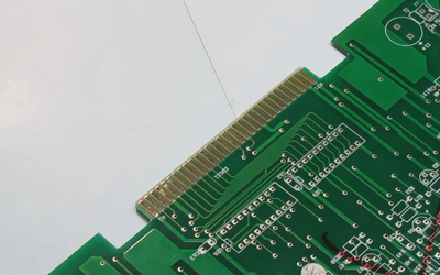
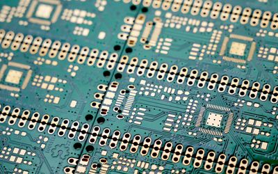
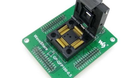
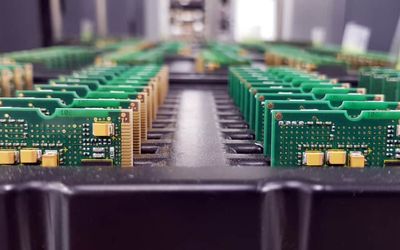
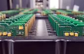
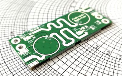
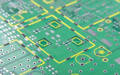
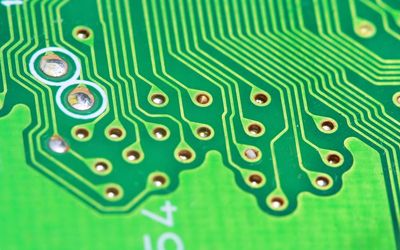
Approximately 7% of the world's gold can be found inside discarded electronic devices, in form of PCB Gold Fingers. While a tonne of Gold Ore produces just 5 grams of pure gold on average, a tonne of electronic scrap can house 300 grams of gold inside it. Here we gloss over the significance of gold fingers in the present day electronics industry and all kinds of gold fingers specifications you need to know.
Tagged with
PCB
ORGANIZATIONS. SHAPING THE INDUSTRY.
HQ NextPCB
Appliances, Electrical, and Electronics Manufacturing
HQ NextPCB specializes in reliable multilayer PCB manufacture and assembly ...
1 Post
AllSpice
Software Development
Hardware collaboration platform 🤖 Inspired by software development princip...
Latest Posts
PCBA design capabilities are crucial to the future of wearable technology. Wearables and PCBA design are inextricably linked since both have a significant influence on each other. As wearable devices become more popular, electronics designers and manufacturers are designing smaller, denser, and more flexible devices.
Vias are small holes in a PCB that enable electrical connections between different layers of the board. In the context of PCB design, via tenting refers to the process of covering the vias with a protective layer, typically a solder mask or dry film. This protective layer shields the vias from environmental factors, such as dust, moisture, and chemicals, which can lead to corrosion or short circuits. As PCB technology continues to advance, the importance of via tenting in maintaining the performance and reliability of complex, high-density interconnect (HDI) and flexible PCB designs cannot be overstated. This guide explores the art and science of via tenting, shedding light on its significance, techniques, and applications in modern PCB design and manufacturing.


