
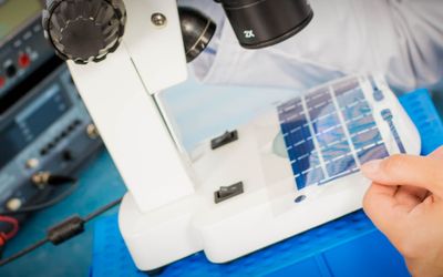
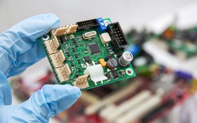
Thin film deposition is a process used to create thin film coatings on different materials. Thin films can consist of metal, semiconductors, and dielectrics, providing them with different properties. These properties translate to benefits such as electrical insulation, optical transmission, and corrosion resistance, that can be used to improve substrate performance. This article explores the processes of thin film deposition, along with its types, parameters, benefits, drawbacks, and applications.
Be the first to know.
Get our pcb weekly email digest.
Tagged with
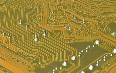
PCB
ORGANIZATIONS. SHAPING THE INDUSTRY.


HQ NextPCB
Appliances, Electrical, and Electronics Manufacturing
HQ NextPCB specializes in reliable multilayer PCB manufacture and assembly ...
1 Post

AllSpice
Software Development
Hardware collaboration platform 🤖 Inspired by software development princip...

Latest Posts

Understanding different modes of diode operation can be critical for designing and implementing electronic systems.

4 minutes read

A new tool to upgrade your embedded processing system to deliver enhanced HMI

Fiducials are reference marks on a printed circuit board that achieve better assembly results.

ABI Research forecasts that TinyML unit volumes will explode from 15 million units in 2020 to 2.5 billion units in 2030. Find out about this machine-learning technique now.
3 minutes read

Filled vias are via holes that are completely filled and closed with conductive or non-conductive material or copper plating. The filled via is one of the many realizations of PCB via covering, specified by industry standards. This article covers the definition, benefits, processes, applications, and challenges of filled vias.
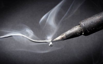
A cold solder joint is a defect caused by improper melting of solder to bond PCB electronic components. This defect can impact the functionality of a PCB assembly, and so must be carefully avoided.
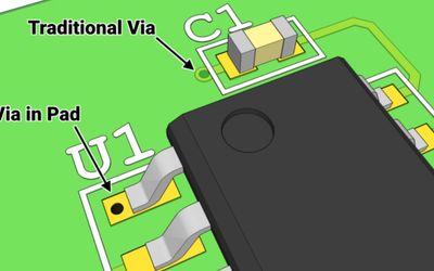
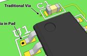
What makes via in pad different from traditional vias? Find out in this short blog.
5 minutes read
Testing PCBs involves using various methods and tools to ensure that all the individual elements of a PCB perform optimally, making up a high-quality PCB assembly. This article delves into the methods, procedures, and requirements of PCB testing.
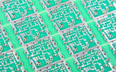
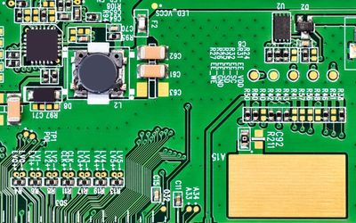
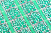
PCB Panelization is a PCB manufacturing technique. It involves the grouping of several small printed circuit boards to form a single array, which is known as a panel. Panelization is commonly employed in PCB manufacturing because it saves time and cost. This article discusses the conditions, design considerations, methods, types, and benefits of PCB panelization.
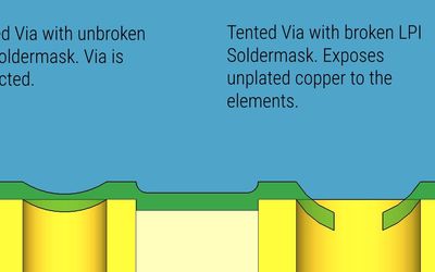
Learn the pros and cons of leaving vias exposed or covered.
4 minutes read

The global trade in counterfeit is worth up to $1 trillion annually, with electronics accounting for a significant portion of that figure. How do you keep your builds counterfeit-free?
4 minutes read

Lead-free solders offer an environment-friendly alternative to toxic lead-based solders, which were dominant in the PCB manufacturing industry till the mid-2000s.

Controlled impedance in printed circuit boards involves the regulation of resistance exerted by signal traces. It is determined by characteristic factors of PCB fabrication, such as trace width and copper thickness. This article discusses controlled impedance and the essentials of its execution in PCB manufacturing.

Before sending your final design files to your CM for manufacturing, check out these useful tips and final steps.
4 minutes read