Nexperia's MLPAK MOSFETs: The Right Fit for Scalable, Application-Driven Designs
Nexperia's MLPAK MOSFETs offer a balanced, scalable solution for modern power and signal designs, combining proven manufacturing, compact form factors, and application-driven performance across consumer, industrial, and embedded systems.

01 Sep, 2025. 7 minutes read
Introduction: Performance and Practicality in Electronics Design
Modern electronics design is increasingly becoming a balancing act. On one hand, engineers are under pressure to reduce form factor, and increase power capability. On the other hand, practical constraints such as cost targets, sourcing stability, and manufacturing throughput are shaping what actually gets built.
Nowhere is this tension more evident than in the selection of discrete components like MOSFETs. Applications such as power supplies, electric motor drives, LED lighting, and consumer electronics, all demand high-efficiency switching devices, ones that deliver reliable performance at the right balance of cost, capability, and availability. In these segments, the challenge is not about pushing absolute limits, but about designing for what’s “right” rather than what’s “best on paper.”
This article explores how Nexperia’s MLPAK family of MOSFETs addresses that challenge. Designed from the ground up to support both power and signal-level use cases, the MLPAK platform focuses on application fit, reliable scaling, and ease of integration. From legacy expertise in discrete semiconductors to modern packaging and inspection techniques, we’ll examine what makes MLPAK a capable, compact, and production-ready solution across diverse end markets.
Legacy of Precision: Nexperia’s Commitment to Quality
Nexperia is not new to the world of discrete semiconductors. With over decades of focused innovation in power devices and a heritage tracing back to Philips Semiconductors, the company has built a reputation around process stability, packaging expertise, and supply reliability.
Much of this precision is rooted in manufacturing excellence. The company’s Manchester site, for example, has been producing semiconductor components for over five decades, while Hamburg’s history stretches back nearly a century. Together they showcase a long-standing engineering heritage that continues to shape its discrete portfolio. Today, that legacy is scaled through modern automation and remains central to Nexperia’s production strategy.

MLPAK is a direct extension of this legacy. By integrating learnings from high-volume production lines, standards, and customer-driven packaging demands, Nexperia has crafted a platform that isn’t just built to spec, it’s built with process maturity in mind.
Suggested reading: 100 years of cutting edge engineering at Nexperia Hamburg plant
Tailoring Components to the Application, Not the Spec Sheet
When it comes to MOSFET selection, design decisions are often influenced by headline specs - ultra-low on-state drain-to-source resistance, sub-nanosecond switching speeds, or thermally advanced packaging. These metrics are critical in high-performance systems. But for many real-world applications, such specifications overshoot what the system actually requires.
Across consumer, industrial, and embedded systems, design engineers increasingly seek components that strike the right balance between meeting functional, thermal, and economic requirements, without unnecessary overhead. It’s not about compromise, but about intentional, well-fitted choices. Whether it’s a low-voltage signal MOSFET in a control circuit or a mid-range switching device in a DC-DC converter, the practical needs shift from peak specs to consistent performance, layout compatibility, and supply chain reliability.
In high-volume designs, the priorities change:
Can this device be reused across stock keeping units (SKUs)?
Is the sourcing secure and scalable over time?
Does it meet thermal and electrical needs without excess margin?
And crucially, does it align with the cost targets that keep the product competitive?
This is the value of application-aligned engineering. Overdesigning can inflate the bill of material (BOM) and complicate layouts. Underdesigning invites failure modes. The sweet spot lies in right-fitting the component, not chasing the spec sheet, but understanding the design context.
With MLPAK, Nexperia offers a portfolio that reflects this shift: MOSFETs in a unified, state-of-the-art footprint, tailored to deliver balanced performance, long-term availability, and integration ease, across both power and signal domains.
Balancing Cost, Form Factor, and Manufacturability
In component selection, lowering cost often comes with compromises like reduced reliability, awkward pinouts, or limited supplier options. Yet, in high-volume applications, managing cost, layout, and scale is not a secondary concern, it’s central to the design process.
The goal for engineers isn’t just to reduce component cost, but to do so without disrupting thermal performance, mechanical compatibility, or production stability. That’s a nuanced challenge, especially when working within industry-standard footprints.
Packaging plays a key role here. It dictates thermal behavior, electrical performance, and manufacturability just as much as the silicon inside. But building a cost-efficient package doesn’t mean cutting corners, it means optimizing construction, assembly, and inspection in ways that scale.
Nexperia’s MLPAK platform is an example of this optimization. With a new package outline design, MLPAK balances performance with production readiness. The result is a family of MOSFETs that maintains electrical and thermal integrity, supports footprint reuse, and fits cost-sensitive designs, all while being designed for scale from the start.
Nexperia’s MLPAK: The Right Fit, by Design
While Dual Flat No-leads (DFN) footprints are widely adopted, and platforms like Nexperia’s LFPAK have long served high-power automotive and industrial needs, not every application requires such performance margins. Many designs, particularly in cost- or space-sensitive segments, demand MOSFETs that balance efficiency, thermal performance, and manufacturability.
Suggested reading: A story of innovation: How LFPAK revolutionized an industry.
MLPAK was developed with this balance in mind. It introduces a scalable packaging that supports both power and signal variants. The product line delivers practical innovation optimized for high-yield, high-volume deployment.

Rather than chasing feature overload, MLPAK focuses on essentials like:
Split Gate Trench (SGT) technology, an advanced trench MOSFET design where the gate structure is split, lowering the gate-to-drain charge and overall gate charge. This enables more efficient switching, reduces Miller plateau effects, and minimizes both conduction and switching losses. In practice, it allows the device to achieve fast, low-loss transitions while maintaining a low RDS(on), which is especially important in high-frequency DC-DC converters, synchronous rectification, and motor control.
Wettable flanks, specially plated sidewalls on the leads that form visible solder fillets, enabling Automated Optical Inspection (AOI). This is crucial for visual verification of solder joints in automotive, industrial, and safety-critical applications, where X-ray inspection is costly or impractical. Select MLPAK MOSFETs are available with wettable flanks, giving designers AOI-ready options where enhanced inspection capability is required. By allowing optical tools to confirm wetting, wettable flanks improve process yield, reduce inspection time, and strengthen traceability in high-volume production.
Support for multiple internal connection approaches, including wire bonding and copper clip bonding, allows a broader variety of package options that can be tailored for performance. Wire bonding remains a flexible and widely used method in higher RDS(on) devices and legacy silicon, while newer technologies, both at Nexperia and across the industry, are increasingly adopting clip bonding for its efficiency and assembly robustness.
MLPAK is a targeted expansion of Nexperia’s discrete portfolio that complements established platforms like LFPAK. While LFPAK devices are engineered for high-end, bespoke solutions that demand maximum robustness, reliability, and performance, many applications simply do not require that level of design margin. MLPAK provides a more versatile alternative so that a single device can serve multiple use cases reliably. It is often the right fit if, delivering the essential performance at the right price-to-performance ratio.
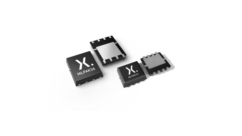
Table 1: Specifications and Key Features of Nexperia MLPAK MOSFETs.
Parameter | Typical Range | Notes |
Package Type | MLPAK33 (3.3 mm x 3.3 mm) / MLPAK56 (5.0 mm x 6.0 mm) | Compact, thermally efficient, wettable flanks for AOI |
Drain–Source Voltage (VDS) | Up to 250 V | Covers low to mid-voltage applications |
RDS(on) | As low as 2.4 mΩ (30V) | Helps minimize conduction losses and supports efficient switching, even with low gate drive voltages. |
Drain Current (ID) | Up to 90 A | Wide current handling for switching, rectification, and motor control |
Total Power Dissipation (Ptot) | ~1.7 W to 80 W | Excellent thermal performance for compact form factor |
Gate Drive Compatibility | Logic-level and Standard-level | Enables integration with low-voltage controllers |
MOSFET Type | N-channel and P-channel | SGT MOSFET technology across both types |
By combining proven process know-how with practical design choices, MLPAK delivers electrical integrity, mechanical reliability, and production efficiency, all in footprints that are familiar to layout engineers and validated across industries.
Built for Manufacturability and Scale
Behind every component in the MLPAK platform is a manufacturing philosophy focused on repeatability, inspection, and scalability. This is not just a product family, it’s a packaging platform engineered to deliver across millions of units without unpredictable cost or quality drift.
Importantly, MLPAK is built within Nexperia’s vertically integrated manufacturing flow, anchored by the company’s backend fab. This allows for tight process control from wafer fabrication to final test and packaging, minimizing sourcing risk while improving quality consistency.
Whether used in consumer electronics, energy-efficient appliances, or safety-critical automotive applications, MLPAK is a packaging platform you can scale, without scaling problems.
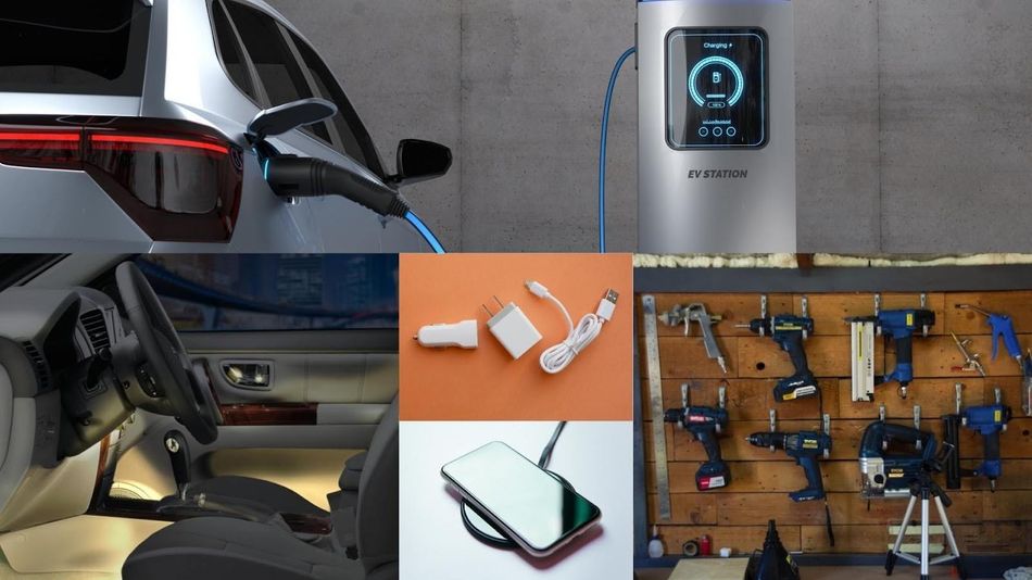
Design Possibilities with Nexperia’s MLPAK33 MOSFETs
The MLPAK platform isn’t tied to a single market or application, it was designed to offer flexibility across both power and signal use cases. With voltage classes ranging up to 250 V, logic- and standard-level gate drive options, and a wide spectrum of RDS(on) values, MLPAK enables engineers to build systems that are compact, efficient, and right for their needs.
Its performance characteristics and manufacturability make MLPAK a strong fit across categories like:
Power Conversion and Switching
DC-to-DC converters in adapters, chargers, and industrial modules
Primary and secondary synchronous rectifiers
Flyback and resonant topologies for space-constrained supplies
Active clamp circuits
Load switches (high-side and low-side) in portable, embedded systems, and body control modules in vehicles
Battery and Power Management
Battery and power Management for power tools, consumer electronics, and electric vehicles (EVs)
USB Power Delivery (USB-PD) adapters
Overcurrent and thermal protection switches for automotive and industrial safety circuits
Motor and Motion Control
BLDC motor drives in fans, pumps, and home appliances
Fan control in industrial and consumer systems
Smart actuators and load controllers in embedded platforms
Motorized functions in vehicles, including window lifts, mirror adjustment, seat positioning, and trunk/door system
Suggested reading: Speeding Up Motor Drive Design, Testing, and Validation with Nexperia Motor Driver Evaluation Kit
Lighting and Auxiliary Systems
LED drivers in architectural, industrial, and appliance lighting
Automotive interior and exterior LED lighting, including headlamps, taillights, and ambient lighting
HVAC control systems and auxiliary rails in both consumer and automotive electronics
Peripheral logic power rails in larger systems and zonal control units in modern cars
Secondary and auxiliary control blocks in white goods and IoT devices
In each of these use cases, MLPAK delivers not by exceeding every metric, but by aligning precisely with what’s needed across production volumes.
Performance Serving Practicality
The MLPAK platform isn’t about pushing boundaries for the sake of it, it’s about delivering meaningful performance where it counts. Built on Nexperia’s decades-long foundation of discrete expertise, MLPAK represents a practical solution for engineers seeking the right fit between electrical performance, physical footprint, and supply chain predictability.
By combining manufacturing maturity, inspection readiness, and thoughtful design choices, MLPAK helps teams build products that are not just technically sound, but scalable and reliable in production. Whether the need is in power conversion, protection, motor control, or auxiliary switching, MLPAK gives engineers a dependable building block, without forcing trade-offs that don’t serve the application.
In a market increasingly shaped by real-world constraints, MLPAK stands out not as a premium outlier, but as an enabling foundation for well-engineered systems at scale.
Unlock the full potential of your electronics design, browse Nexperia’s complete MLPAK33 and MLPAK56 MOSFET lineup: MLPAK33 MOSFETs | MLPAK56 MOSFETs
References
[1] Jiang J. Optimized power switching for high-volume applications [Internet]. Efficiency Wins; 2025 Apr 23. Available from: https://efficiencywins.nexperia.com/efficient-products/optimized-power-switching-for-high-volume-applications