Vcc vs Vdd: Differences, Usage, and Best Practices in Modern Electronics
This article is a detailed guide on Vcc vs Vdd power rail naming conventions in analog and digital circuits (CMOS vs bipolar), with practical tips for schematics, PCB layout, and IC selection!

22 Apr, 2025. 13 minutes read
Printed Circuit Board (PCB)
Introduction
In modern electronics, understanding power supply terminology is critical for accurate circuit design and analysis. The most frequently encountered terms are Vcc and Vdd, both of which refer to voltage supply rails but differ significantly in context and application. The distinction between Vcc vs Vdd reflects the underlying transistor technology (BJT vs. MOSFET) and impacts everything from schematic labeling to voltage regulation strategies. Ultimately, a clear understanding of Vcc vs Vdd contributes to more robust and reliable electronic designs.
In this article, we’ll explore the technical differences between Vcc vs Vdd, discuss their historical origins, and examine how each is used in analog and digital circuits today. Additionally, we’ll provide best practices for choosing and labeling power rails correctly, especially in mixed-signal and integrated circuit designs where the confusion between Vcc vs Vdd can lead to costly mistakes!
Understanding Vcc vs Vdd: What Do These Symbols Mean?
In electronic circuits and datasheets, notations like Vcc, Vdd, Vss, and Vee are commonly used to label power pins or rails. These terms originate from transistor technology and reflect the voltage at a certain transistor terminal in the circuit.
The letters themselves hint at the transistor element referenced:
Vcc stands for “Voltage at the Collector” and is traditionally used in bipolar junction transistor (BJT) circuits. It typically denotes the positive supply voltage connected to the collector terminal of an NPN transistor. In most BJT-based analog circuits and TTL logic, Vcc is the primary power supply rail.
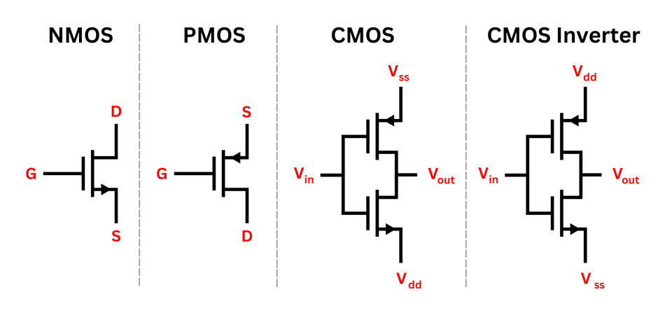
Vdd refers to “Voltage at the Drain”, used in field-effect transistors (FETs) such as MOSFETs. In CMOS logic and modern digital circuits, Vdd is the supply voltage connected to the drain terminal of an n-channel MOSFET. [1] It commonly powers the logic core of ICs, including microcontrollers and FPGAs.
Vss stands for “Voltage at the Source” and usually represents GND or the negative supply voltage in FET-based circuits. In most CMOS designs, Vss is tied to 0 V and serves as the common reference point.
Vee means “Voltage at the Emitter” and is used in bipolar circuits, especially for the emitter of PNP or NPN transistors. It typically denotes the negative rail or ground in op-amp and analog amplifier designs.
These naming conventions stem from how different transistor types are biased in a circuit! While Vcc vs Vdd both usually refer to positive supply voltages, their usage depends on the technology: Vcc for BJTs, and Vdd for MOSFETs. Similarly, Vss and Vee correspond to the source or emitter side and usually point to GND or a negative supply.
The table below summarizes these naming conventions and their typical usage in circuits:
| Symbol | Meaning of Subscript | Typical Role | Example Usage |
| Vcc | Voltage at Collector | Positive supply in BJT circuits (also used generally in many ICs) | +5 V supply on a TTL logic IC labeled as Vcc; VCC pin on an op amp for +V |
| Vdd | Voltage at Drain | Positive supply in MOSFET/CMOS circuits (digital logic, CMOS ICs) | +3.3 V supply for a microcontroller labeled VDD; VDD on a CMOS logic chip |
| Vee | Voltage at Emitter | Negative supply in BJT circuits (or ground in single-supply BJT circuits) | -5 V on an analog amplifier labeled VEE; or 0 V ground in a single-supply BJT circuit |
| Vss | Voltage at Source | Ground or negative supply in FET/CMOS circuits | 0 V ground pin on a CMOS IC labeled VSS; negative rail on a MOS-based analog chip |
| GND | Ground (zero reference) | Common return/reference node (0 V) | Power ground on a PCB, often tied to Vss or Vee in the circuit |
It’s important to remember that these symbols are conventions, not fixed voltages. For instance, Vcc doesn’t always mean +5V—it might be +3.3V or even +1.8V, depending on the IC. Similarly, a Vdd label could refer to a supply voltage anywhere from 1.0 V to 5.5 V. Always consult the datasheet for exact voltage requirements and tolerances.
You might also encounter labels like V+, V-, or Vbb (voltage at base), especially in analog circuits, power amplifiers, or biasing configurations. However, this article focuses primarily on Vcc vs Vdd, as these are the most widely used and often misunderstood terms in modern electronic circuits.
Recommended Reading: VSS vs VDD: Understanding Power Rails in Electronic Circuit Design
CMOS vs Bipolar Transistor Conventions (Drain vs Collector)
The use of Vcc or Vdd in a circuit schematic often hints at the underlying transistor technology. These naming conventions are rooted in historical distinctions between bipolar junction transistors (BJTs) and field-effect transistors (FETs), particularly MOSFETs.
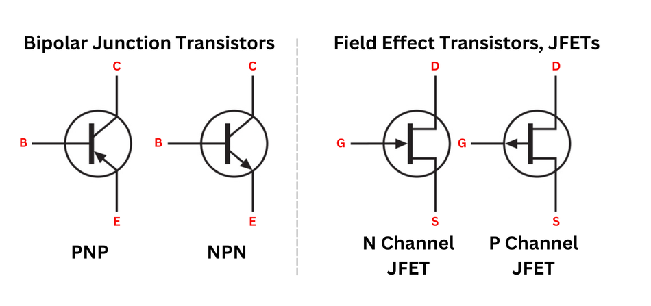
Bipolar Junction Transistor (BJT) circuits
In bipolar circuits, the terminology is straightforward:
Vcc refers to the collector voltage, typically the positive supply voltage in NPN transistor configurations.
Vee indicates the emitter voltage, often the negative supply voltage, or in single-supply systems, tied to GND (0 V).
Classic analog amplifiers, TTL logic circuits, and op-amps built from BJTs follow this convention. For example, in a 5 V TTL system, Vcc = +5 V and Vee = 0 V (GND). In dual-supply applications, labels like Vcc+ and Vee− may be used to represent both rails. Many analog devices, even those now implemented in CMOS, continue using Vcc/Vee to maintain legacy compatibility.
Field-Effect Transistor (FET) circuits
With the shift to MOSFET and CMOS technologies in digital circuits, a new convention emerged:
Vdd stands for the drain voltage, or positive power supply in FET circuits.
Vss refers to the source voltage, typically tied to GND in n-channel designs.
In an NMOS circuit, the drain terminal connects to Vdd, and the source terminal connects to Vss, which is often ground. When CMOS (Complementary MOS) emerged—using both n-channel and p-channel MOSFETs—the Vdd/Vss terminology became standard, even though both supply voltage rails technically connect to sources: the P-MOS source is at Vdd, and the N-MOS source is at Vss. Despite this inconsistency, the naming persisted. [2]
In modern designs, these conventions often blur! Integrated circuits today frequently integrate both BJTs and MOSFETs or contain mixed-signal functionality. Resultantly, you might find Vcc on a purely CMOS-based chip or Vdd on a microcontroller that internally uses BJTs. For example, some analog ICs built with CMOS still label their positive supply as Vcc, and vice versa. The important takeaway is that Vcc and Vdd both refer to the positive supply rail, and their usage is often interchangeable in practice.
To illustrate the conventions, consider a simple logic inverter implemented in different technologies:
Let’s compare two examples:
In a CMOS inverter, the P-MOSFET connects to Vdd, and the N-MOSFET connects to Vss. When the input is low, the output is pulled to Vdd; when the input is high, the output is pulled to Vss.
In a BJT inverter, the collector connects to Vcc through a resistor, while the emitter goes to GND. A high base input switches the transistor on, pulling the output toward the ground.
Although the circuit behavior is different due to transistor type, the supply voltage function remains the same. Whether it’s Vcc vs Vdd, both provide the operating voltage to the circuit.
Recommended Reading: JFET vs MOSFET: A Comprehensive Engineering Analysis and Selection Guide
Are Vcc and Vdd Interchangeable?
From a technical perspective, Vcc should be used for bipolar circuits, and Vdd for MOS-based ones. But in modern practice, these terms are often used interchangeably to indicate the positive supply voltage. What matters most is consistency within your schematic, PCB labels, and datasheet references.
You’ll commonly see a microcontroller refer to its 3.3V rail as Vdd, while a development board silkscreens the same voltage as Vcc. In essence, these labels—Vcc, Vdd, Vee, Vss—are shorthand to help engineers quickly identify power supply connections, but the actual voltages must always be verified against the datasheet of the device.
Recommended Reading: Understanding NPN vs PNP Transistors: A Comprehensive Guide
Roles of Vcc/Vdd in Circuits and Typical Voltages
Regardless of whether a pin is labeled Vcc or Vdd, its fundamental role is the same: to provide the power supply voltage required by the circuit’s active components, such as transistors, ICs, and other semiconductor devices. These supply pins create the electrical potential between the positive rail (Vcc/Vdd) and the ground/reference (Vss/Vee or GND)—a crucial operating condition for every electronic device.
Here we outline the roles and typical voltage levels in various contexts:
Digital Logic (TTL, CMOS, etc.)
In digital circuits, the Vcc/Vdd rail powers logic elements such as gates, flip-flops, and timing modules. For TTL and other bipolar logic families, Vcc is traditionally set at +5V, aligned with the typical collector voltage in NPN transistor configurations. On the other hand, CMOS families like 74HC or 74LVC often operate at voltages ranging from 2V to 5V, though their datasheets may still use the Vcc label for legacy compatibility. [3]
Modern microcontrollers and microprocessors typically use Vdd to denote the main supply voltage for the digital core and I/O subsystems. Common values include 3.3V or 5V, though newer low-power MCUs may operate at just 1.8V. High-performance processors and FPGAs feature multiple Vdd rails, such as:
Vdd_core ≈ 1.0V – For the internal logic.
Vdd_io = 1.8V or 3.3V – For external interfaces.
These rails are often labeled as VCCINT, VCCIO, or similar, indicating functional domains. The specific voltage levels must always be verified in the component’s datasheet, as the Vcc vs Vdd label does not dictate the voltage value.
Analog Circuits (Op Amps, Amplifiers, ADCs)
In analog circuits, particularly in op-amps, amplifiers, and ADCs, the power supply requirements vary. You’ll encounter a mix of naming conventions:
Bipolar-based analog ICs use Vcc (positive) and Vee (negative) to describe their rails.
CMOS analog ICs adopt Vdd and Vss for the same purpose.
For example:
The classic 741 op-amp operates from ±15V supplies, labeled VCC+ and VCC-.
A CMOS analog switch may use Vdd = +5V to +8V and Vss = -5V to -8V.
In single-supply analog systems, Vss or Vee is tied to 0V, and only the positive supply voltage is provided (e.g., Vdd = +5V, Vss = 0V). This configuration is common in portable devices and sensor interfaces, where minimizing power consumption is critical.
Mixed-Signal and Complex ICs
In mixed-signal ICs, such as motor drivers, MCUs with analog features, and communication transceivers, multiple power domains often coexist:
One rail may power digital logic (e.g., Vdd = 3.3V).
Another may support analog, motor drive, or high-voltage sections (e.g., Vcc = 15V)
Take the STMicroelectronics STSPIN32G0 as an example. The datasheet shows:
VDD = 3.3V for the microcontroller.
VCC = 15V for the motor control stage (often containing MOSFETs or BJTs).
Similarly, microcontrollers like the ATmega328P feature separate analog supply pins:
AVCC – Analog Vcc for ADC and analog blocks.
Microchip PICs – Often feature AVDD and AVSS for analog power and ground.
The presence of multiple Vcc/Vdd labels in one device emphasizes the importance of clear voltage mapping in schematics and PCB design.
Typical Voltage Levels in Modern Systems
| Voltage Level | Typical Use Case |
| 5V | Legacy TTL, some bipolar microcontrollers, interface circuits, and sensors |
| 3.3V | Standard for modern digital circuits, CMOS logic, MCUs, memory cards, etc. |
| 1.8V / 1.2V | Low-power cores in FPGAs, CPUs, and SoCs to reduce power consumption |
| ±12V / ±5V | Analog amplifiers, op-amps, RS-232 transceivers, and older analog interface circuits |
| 0V (GND) | Reference node for Vss, Vee, or ground. Used across both analog and digital circuits |
Modern electronics often have multiple power rails, and naming them clearly is vital. In a smartphone or embedded system, you might encounter numerous power rails like 1.0V, 1.8V, 3.0V, or 3.8V, each labeled by function (e.g., Vdd_CPU, VBAT, VIO) to avoid ambiguity.
Recommended Reading: Understanding NPN vs PNP Transistors: A Comprehensive Guide
Reading Datasheets: Conventions and IC Selection Implications
When selecting components or reading their datasheets, the way power pins are labeled can give you clues about the IC’s internal technology or heritage, but more importantly, it tells you how to hook it up correctly.
Here are some practical notes:
1. Identify the Supply Pins
Every datasheet pinout will specify one or more supply rails, typically labeled Vcc, Vdd, Vss, or Vee. These labels direct you where to connect your supply voltage and ground (GND). Some chips may simplify the naming to V+ and V-, while others—especially mixed-signal ICs—may list multiple distinct supplies (analog, digital, core, or I/O).
If the pinout uses Vdd and Vss, this strongly suggests a CMOS or MOSFET-based design.
If it uses Vcc and GND, the chip may be based on bipolar transistors or simply follow TTL-style conventions.
For example:
Microchip PIC microcontrollers consistently use VDD (positive) and VSS (ground), clearly indicating their CMOS architecture.
Atmel AVR microcontrollers, like the ATmega328P, use VCC and GND, even though internally they are CMOS devices. This naming convention is likely retained from their legacy 5V TTL usage.
The Vcc vs Vdd distinction is semantic—what matters is the voltage level indicated in the electrical characteristics table, not the label itself.
2. Technology Clues from Naming
While not a rule, supply labeling often reflects internal design choices:
Vdd/Vss: Typically indicates a CMOS architecture, often supporting wide voltage ranges, low leakage currents, and rail-to-rail operation.
Vcc/Vee: Commonly associated with bipolar designs or older analog ICs, sometimes implying higher power draw or different signal swing behavior.
For example:
An Analog Devices analog switch may use Vdd/Vss, suggesting CMOS internals designed for full-range analog signal control.
In contrast, a linear regulator showing Vcc may be bipolar, optimized for stable operation in traditional analog circuitry.
This difference may influence design decisions — CMOS op-amps using Vdd/Vss often excel at low-voltage operation, whereas bipolar op-amps using Vcc/Vee can offer a better linear response in ±15V systems.
3. Checking Supply Voltage Ratings
Never rely solely on the Vcc/Vdd label to assume a safe voltage. Instead, inspect the electrical characteristics in the datasheet:
A logic gate may list “Supply Voltage (VCC) = 2.0V to 6.0V.”
A microcontroller might state “VDD = 1.8V to 5.5V; VSS = GND.
This is especially critical when working with low-power MCUs or high-speed FPGAs, where incorrect supply voltage can lead to erratic operation or damage.
For example, a 5V-only device labeled with Vcc cannot be powered by a 3.3V rail, regardless of its name.
4. Multiple Supply Domains in Complex ICs
Modern ICs—particularly microcontrollers, FPGAs, and analog-digital converters—often use more than one supply voltage, labeled with functional prefixes:
| Label | Description |
| AVcc / AVdd | Analog supply voltage—used for ADCs, DACs, and analog comparators |
| DVcc / DVdd | Digital supply—powers logic or CPU cores |
| VCCIO | Supply for I/O voltage levels |
| VCORE / VDDCORE | Internal logic supply for cores, often lower (e.g., 1.0V or 1.2V) |
| VCCA | Analog or PLL supply in digital chips |
For example, the ATmega328P requires AVCC to be connected even if the ADC isn’t used—per the datasheet. [4] Similarly, FPGAs like Xilinx or Intel Cyclone series may have VCCINT for the core and VCCIO for I/O banks, requiring careful voltage domain separation.
It is important to follow datasheet guidelines regarding filtering (e.g., inductors or ferrite beads) to minimize power rail noise between domains.
5. IC Selection and Search Filters
Component databases and distributors may use either Vcc or Vdd in filters. Whether it says “Vcc (max) = 5V” or “Vdd = 3.3V,” always match the numeric value to your design supply rail.
Don’t worry if your board uses a mix of ICs labeled Vcc, Vdd, or V+—if they all operate from a shared +5V supply, it’s fine to tie them to the same rail, often labeled generically as +5V or Vcc on your schematic or PCB.
Recommended Reading: FPGA vs. Microcontroller: Understanding the Key Differences
PCB Implementation and Labeling Practices
When it comes to actually building the circuit on a PCB, the goal is to correctly distribute these supply voltages and label them clearly to avoid mistakes.
Here’s how Vcc and Vdd play out in schematic capture and PCB layout:
1. Schematic Net Naming Conventions
EDA tools allow designers to name supply nets freely. It’s common to use labels like VCC, VDD, +5V, or +3V3 to denote the positive supply rail. While the net name doesn’t affect electrical functionality, consistency improves readability and reduces errors.
If your microcontroller’s datasheet uses VDD/VSS, it's good practice to mirror those names in your schematic to match the manufacturer’s convention. For example:
Label the 3.3V net as VDD.
Label ground as VSS or GND.
Alternatively, some designs avoid transistor-centric labels altogether and use explicit voltage identifiers like +5V or 3V3. This is especially common in Arduino-style or open-source hardware projects.
2. Silkscreen Labels and Connectors
On the PCB silkscreen, clearly mark all power input points, test headers, and connectors. Labels like 5V, VCC, and GND are standard and help technicians quickly identify power lines during debugging or assembly.
If your board has multiple supplies, qualify them (e.g., VCC_5V, VCC_3V3, or AVCC, DVCC).
Use GND as the universal label for ground, even if the internal IC labels it VSS or VEE.
In dual-supply designs, label accordingly: +VCC, -VEE, etc.
This kind of labeling enhances safety and clarity during system integration and testing.
3. Examples in Practice
A board may have headers labeled “VBB, GND, +5V,” where VBB is a bias voltage, GND is the reference, and +5V acts as the Vcc for logic devices.
Another may show “VCC, GND, VEE,” indicating a positive, ground, and negative supply—likely used in an analog amplifier or op-amp configuration.
These examples reflect both traditional bipolar and CMOS naming conventions, which often coexist on modern mixed-technology boards.
4. Decoupling and PCB Layout Guidelines
No matter what you call the supply voltage, proper decoupling is critical. Always place ceramic capacitors (e.g., 0.1 µF) close to each Vcc/Vdd pin on an IC—with short traces to GND.
If your microcontroller has multiple Vdd/Vss pins (e.g., on opposite sides of the package), connect and decouple all of them. This is especially important in high-speed digital circuits to maintain voltage stability.
Use short, wide traces or power planes for Vcc/Vdd routing.
Always route the decoupling path as: Vcc/Vdd → capacitor → ground, not in parallel from a distant trace.
Failure to decouple every supply pin as specified in the datasheet can lead to voltage ripple, noise, or functional errors—even if the chip powers up.
5. Grounding in Mixed-Signal Designs
In mixed-signal PCBs, it's common to separate analog ground (AGND) and digital ground (DGND). These grounds might only meet at a single star point or through a ferrite bead, minimizing digital noise in sensitive analog sections.
The Vcc/Vdd labeling plays a role here:
Use AVcc / AVdd for the analog power supply.
Use DVcc / DVdd for the digital supply.
Similarly, label AVss / AVee and DVss / DVee as separate references if needed.
Such separation helps maintain signal integrity, especially in systems involving ADC, DAC, or high-resolution op-amp circuitry.
6. External Power Connectors and Regulators
If your board accepts external power (e.g., through a barrel jack or USB), define clear naming conventions:
Use VIN to represent the raw input voltage before regulation (e.g., 7–12V).
The output of a regulator (e.g., 5V) can be labeled VCC or VDD, depending on preference.
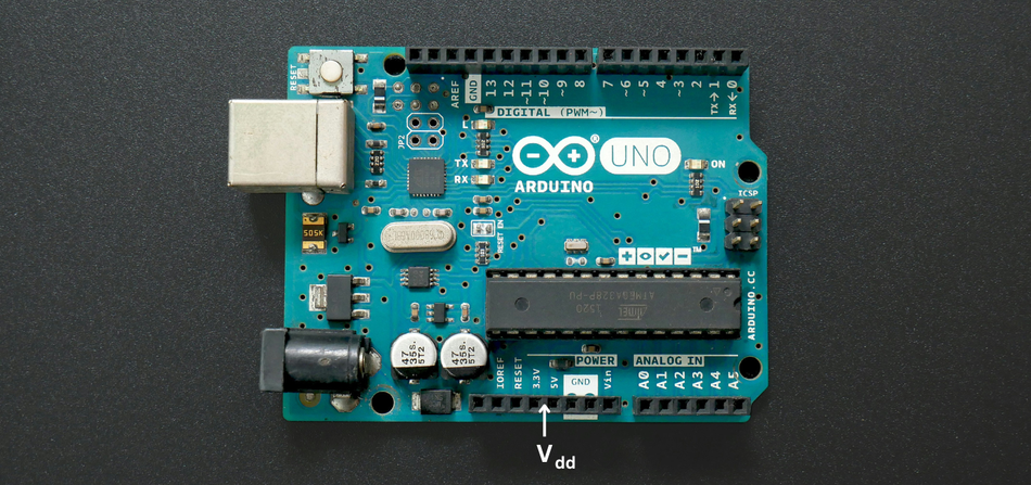
For example, an Arduino Uno uses VIN for the unregulated input and generates VCC = 5V via an onboard regulator. This 5V then supplies all ICs and peripherals on the board.
So, avoid confusing VIN (unregulated) with Vcc (regulated). Maintain this distinction in both the schematic and silkscreen.
Recommended Reading: PCB Silkscreen: What is it?
Conclusion
In modern electronics, Vcc vs Vdd is more than just a labeling difference—it reflects the transistor technology and design history behind a circuit. While Vcc stems from bipolar junction transistors and Vdd from MOSFETs, both denote the positive supply voltage essential for powering ICs. Similarly, Vss and Vee represent the reference or ground rails, completing the circuit.
Understanding these conventions ensures accurate schematic reading, correct PCB connections, and better communication in design documentation. Whether you’re designing with analog op-amps, digital microcontrollers, or mixed-signal ICs, make sure to match supply voltage values to device requirements—not just the labels.
Adopt consistent naming across your design, consult the datasheet, and verify all supply and ground pins are properly connected and decoupled. By mastering this foundation, you’ll avoid costly errors and design smarter, cleaner, and more robust electronic systems.
Frequently Asked Questions (FAQs)
Q: What is the difference between Vcc and Vdd?
A: Vcc originates from BJT circuits (collector), while Vdd comes from FET circuits (drain). Both supply positive volts to the IC. Though rooted in different transistor types, they serve the same purpose: providing the power source for the chip’s logic, regardless of whether it's analog or real-time digital.
Q: What do Vss and Vee mean?
A: Vss refers to the source terminal in MOSFET-based circuits—usually tied to ground or 0 V. Vee applies to bipolar designs, connected to the emitter, often acting as a negative voltage reference. Both establish a common point for polarity and signal return in analog and digital circuits.
Q: Are Vcc and Vdd the same thing (can I treat them interchangeably)?
A: In most electronic circuits, yes! Vcc and Vdd both serve as the positive supply rail, regardless of label. Just ensure voltage consistency across the schematic. However, if a design has multiple supplies (e.g., 1.2V core, 3.3V I/O), mixing labels without clarification could cause serious polarity confusion.
Q: Why do some datasheets use Vcc while others use Vdd for the supply pin?
A: It depends on manufacturer conventions and transistor technology. Older operational amplifiers and bipolar ICs often use Vcc, while modern CMOS and microcontrollers use Vdd. Regardless, datasheets clearly define supply voltage, ensuring correct connection to your power source during real-time application or simulation.
Q: Does Vcc always refer to +5 V?
A: No! While +5 V was common in early TTL logic, Vcc now ranges from 1.0 volts to 12 volts, depending on the IC’s power source. For example, a common collector amplifier might use Vcc = 12V, while a microcontroller operates safely from 1.8 V to 5.5 V.
Q: How should I connect and decouple Vcc/Vdd pins on a circuit?
A: Connect each Vcc/Vdd to the correct power source, and add decoupling capacitors close to the IC. This reduces noise and supports stable operation, especially in real-time systems. Always follow the datasheet’s guidance to maintain voltage stability and prevent issues in operational amplifiers or digital logic.
Q: What about other labels like Vpp or Vbb?
A: Vpp is often a voltage reference for programming (e.g., 12 V), while Vbb denotes a bias voltage at the base in bipolar logic or analog design. These are application-specific and not interchangeable with Vcc/Vdd. Always check the datasheet to match voltage level and polarity correctly.
References
[1] Wevolver. VSS vs VDD: Understanding Power Rails in Electronic Circuit Design [Cited 2025 April 14] Available at: Link
[2] Wevolver. PMOS vs NMOS: Unraveling the Differences in Transistor Technology [Cited 2025 April 14] Available at: Link
[3] Onsemi. Interfacing to MM74HC High-Speed CMOS Logic [Cited 2025 April 14] Available at: Link
[4] Microchip Technology. ATmega328P Detailed [Cited 2025 April 14] Available at: Link
in this article
1. Introduction2. Understanding Vcc vs Vdd: What Do These Symbols Mean?3. CMOS vs Bipolar Transistor Conventions (Drain vs Collector)4. Roles of Vcc/Vdd in Circuits and Typical Voltages5. Reading Datasheets: Conventions and IC Selection Implications6. PCB Implementation and Labeling Practices7. Conclusion8. Frequently Asked Questions (FAQs)9. References