Circuit Symbols: A Comprehensive Guide for Electronics Engineers
An in-depth exploration of schematic circuit symbols, their standards, uses in design, and best practices – ideal for digital/hardware engineers and engineering students.

08 Apr, 2025. 20 minutes read
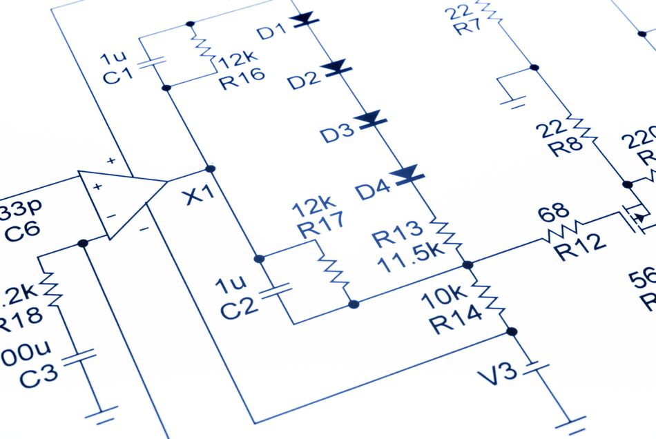
A circuit diagram featuring various component symbols
Key Takeaways:
Circuit symbols are the standardized graphical language of electronics. They represent components (e.g., resistors, transistors, and logic gates) in schematics for clear communication.
American schematic diagrams follow established standards (e.g., IEEE/ANSI symbols) so that engineers everywhere can interpret and design circuits consistently.
Understanding schematic symbols is essential for circuit design, analysis, and troubleshooting – it enables engineers and students to read complex circuit diagrams as easily as reading a map.
Best practices for using circuit symbols include consistent use of standard symbols, clear labeling of components and connections, and organized schematic layouts (inputs left, outputs right, power at top, ground at bottom) .
Common mistakes to avoid include misinterpreting symbols, misreading connection dots, overlooking power/ground references, and using non-standard or inconsistent symbols.
Introduction
Ever looked at an electronic schematic and wondered what all those squiggly lines and odd shapes mean? If so, you’re not alone. Those little shapes are circuit symbols, and together, they form the universal language of circuit design. Each symbol is a pictogram representing an electrical component or function – for example, a zigzag line for a resistor or a triangle arrow for a diode.
Engineers rely on these electrical schematic symbols to convey complex circuits in a clear, concise way, rather than drawing realistic pictures of each component. In fact, designers and hardware engineers must have a common language to describe the parts of a project – and circuit symbols provide an unambiguous way to show each component’s type and function in a diagram . Learning this language is a crucial step for anyone in electronics, from students building their first circuits to seasoned digital design engineers collaborating on multi-million-transistor hardware.
Suggested Reading: How to Read a Circuit Board: Mastering the Language of Electronics
Theoretical Foundation of Circuit Symbols
Circuit symbols serve as an essential abstraction in electrical engineering, allowing complex component behaviors, often described by intricate physics and mathematics, to be represented by simple graphical drawings. This simplification enables engineers to visualize electronic functions without constantly dealing with integrals and derivatives, significantly facilitating communication and reasoning about circuits. Many early symbols cleverly incorporated visual cues related to the component's physical form or its function. For instance, the resistor's zigzag line hinted at resistance, the inductor's loops resembled a coil, and the capacitor's parallel lines mirrored its physical structure. As technology progressed, new symbols for devices like diodes and transistors emerged, with shapes designed to suggest their operational characteristics, such as the diode's directional current flow or the transistor's control terminals.

The advent of the digital era necessitated entirely new, more abstract symbols for logic gates and other boolean functions. These distinctive shapes, like the D for AND and the curved shield for OR, were established by early standards to ensure uniformity and easy recognition on complex schematics. A dedicated committee formalized these graphical representations, ensuring that engineers across the field would consistently interpret and draw circuit diagrams. This evolution has resulted in a comprehensive and universally understood language of circuit symbols, where each simple drawing encapsulates decades of design consensus, transforming the schematic into a truly universal document for electrical engineers.
Standard Circuit Symbols in American Schematics (IEEE/ANSI Standards)
In the United States (and many other regions by influence), circuit diagrams adhere to a set of standard symbols defined by organizations like IEEE and ANSI. The goal is that anyone reading the schematic will recognize the symbols immediately. The primary reference for American circuit symbols has historically been ANSI Y32.2 / IEEE Std 315 (originally released in 1975), titled “Graphic Symbols for Electrical and Electronics Diagrams.” This standard (often just called IEEE 315-1975) compiled the accepted symbols for virtually every electrical component at the time – from basic components to logic symbols and beyond. For decades, IEEE 315 has been the definitive guide for schematic symbols in the U.S., and its notation is still widely taught and used. (Interestingly, IEEE 315 was officially deprecated in 2019 with no direct replacement, but engineers continue to reference it since the symbols remain industry standard .) In addition to IEEE 315, there have been specialized standards like IEEE Std 91 (covering logic gate symbols for digital electronics) that complement it.

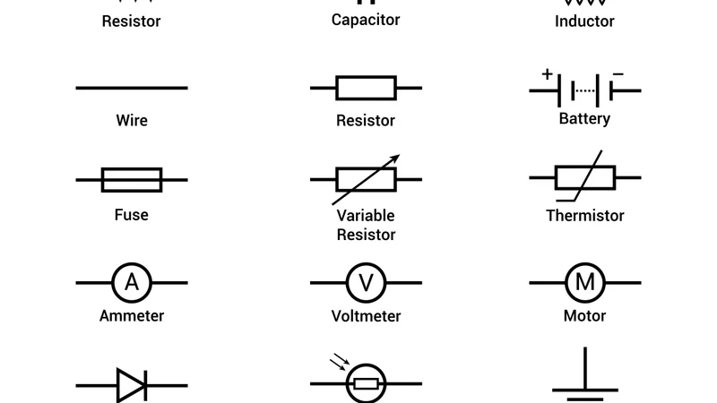
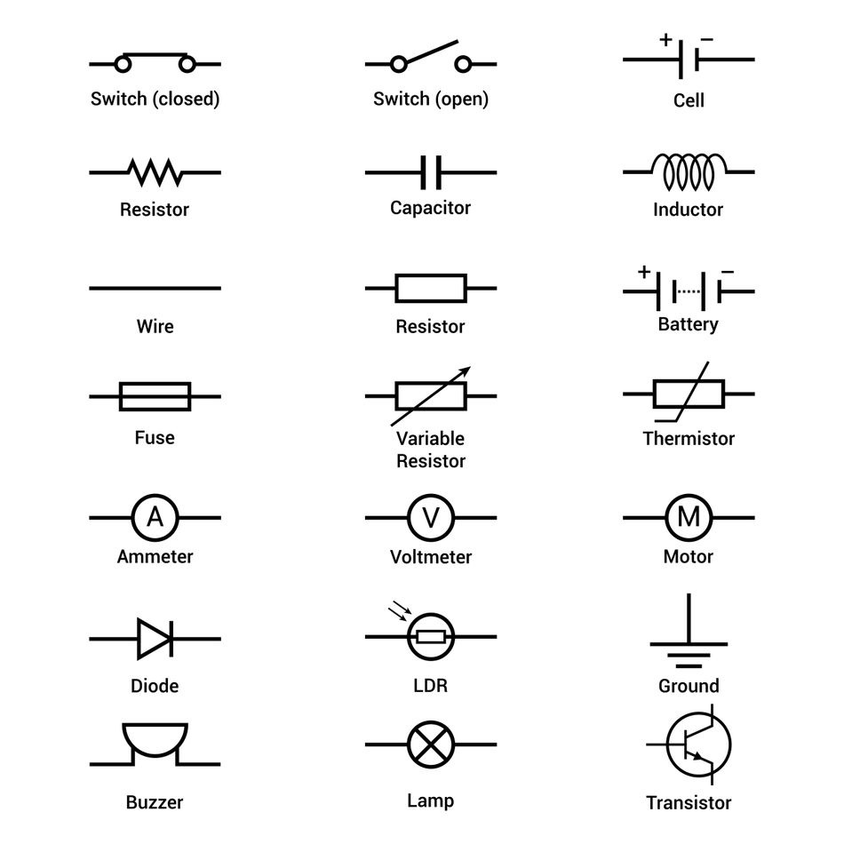
Let’s look at some of the common circuit symbols you’ll encounter, along with their meanings. We will focus on the American-style symbols as per IEEE/ANSI conventions (which are also the ones most widely used in industry and education). Remember, each symbol represents a specific electronic component or function:
Wire/Connection: Lines in a schematic represent wires or connections between components. When two wires connect, a dot or node is placed at the junction. (No dot where lines cross means they are not connected – more on that in best practices.)
Ground: The symbol for ground (common reference point in the circuit) is usually a set of three descending horizontal lines (the longest at top). This indicates a connection to the circuit’s 0V reference or chassis. Another ground variant is a triangle symbol (often used for signal ground in some schematics). All denote a return path/common node for currents.
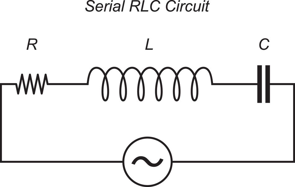
Resistor: A small zigzag line is used to represent a resistor. This zigzag shape intuitively signifies something impeding the flow of electricity. In American schematics, this is the standard symbol for a fixed resistor. (Each resistor symbol is usually labeled with an “R” and a number like R1, plus a value in ohms.)
Capacitor: Two short parallel lines denote a capacitor (which stores charge). It looks like a tiny version of capacitor plates. For a polarized capacitor (electrolytic), one of the lines may be curved or a + sign may be added to indicate the positive side.
Inductor (Coil): A series of looping curves (often drawn as a series of semicircles or loops) represents an inductor or coil. This mimics the appearance of a coiled wire, indicating a component that stores energy in a magnetic field.
Diode: A diode is shown as a triangle pointing to a line. The triangle points in the direction of conventional current flow (from anode to cathode), and the vertical line represents the diode’s barrier that current cannot cross in the opposite direction. A special diode like an LED (light-emitting diode) may be drawn with the same symbol plus two little arrows emanating out to indicate light.
Transistors: Transistor symbols vary by type. A Bipolar Junction Transistor (BJT) is drawn as a combination of a straight line (the base) with two diagonal lines (emitter and collector) forming a sort of T-shape; one of the diagonals has an arrow indicating emitter direction (arrow out for NPN, in for PNP). Field-effect transistors (FETs) have their own standard symbol (a line for the channel with source, drain, and a gate symbol). While the details can look complex at first, each part of the symbol corresponds to transistor terminals and how they connect.
Integrated Circuit (IC): In schematics, complex ICs (like microcontrollers, op-amps, logic chips) are often drawn as simple rectangular blocks with pin numbers or labels. However, fundamental elements inside them (for example, an Op Amp symbol) have a distinctive shape – an op-amp is typically shown as a triangle with the point on the output side, a + input and – input on the left, and often +V/–V power pins at top and bottom of the triangle.
Logic Gates: Digital logic gates use distinctive-shape symbols. For example, an AND gate is drawn as a D-shaped curved outline (flat on the left where inputs enter, rounded on the right where the output exits). An OR gate looks like a curved shield that tapers to a point on the right. A NOT gate (inverter) is a triangle pointing right with a small bubble (o) at its tip to indicate inversion. Combining these, a NAND gate is an AND gate with a bubble on its output, and a NOR gate is an OR gate with a bubble on the output (the bubble means “NOT”). An XOR gate is an OR gate symbol with an extra curved line on the input side (indicating “one or the other but not both”), often labeled with “=1” on its output in some standards. These logic symbols were standardized by IEEE 91 and are widely used in schematics for digital circuits.
It’s worth noting that the IEEE/ANSI symbols are widely accepted in the U.S. and in many international contexts, even though the IEC (international) standard symbols exist as well. For example, the resistor’s zigzag is the IEEE symbol; in the IEC standard used in some countries, a resistor might be drawn as a simple rectangle – but the meaning is the same (a resistance).
Suggested Reading: PCB Components: A Comprehensive Technical Guide to Passive, Active, and Electromechanical Parts
In American schematic diagrams, every symbol is typically accompanied by a reference designator (a label like R, C, L, U, etc., with a number) and often a value or part number. For example, near a resistor symbol, you might see “R5 10k,” meaning resistor number 5 with a value of 10 kΩ. Capacitors might be “C1 10µF” for a 10 microfarad capacitor, and integrated circuits might be “U3,” etc. These designators are standardized (R for resistor, C for capacitor, L for inductor, D or CR for diode, Q for transistor, U for IC, etc.) . They help you cross-reference the schematic with parts lists and PCB layouts. So, as you read a schematic, not only do the symbols tell you what the component is, but the labels and values tell you which specific component and its rating. Together, the symbol shapes and the annotations give a complete picture of the circuit’s design.
Practical Applications of Circuit Symbols in Design and Analysis
Knowing the theory and shapes of circuit symbols is one thing, but using them effectively is another. In practice, circuit symbols are the building blocks of schematics, and schematics are used at every stage of electronics design and analysis. Let’s explore how a design engineer or student applies this knowledge:
Reading Schematics (Circuit Analysis): Being able to read a schematic diagram is a fundamental skill in electronics. When you see a page full of symbols connected by lines, you are essentially reading a map of an electronic circuit. For instance, a hardware engineer troubleshooting a board will consult the schematic to understand how the components are connected. By tracing from one symbol to the next via the drawn connections (nets), you can follow the flow of electricity through the circuit – from the power source symbol, through various components, to ground. This allows you to understand how the circuit is supposed to work, identify where a signal goes, or locate a point of failure.
Designing Circuits (Schematic Capture): When engineers design new circuits, they actually draw schematics using these symbols as the first step (often using CAD software). The engineer will place symbols for each component (or select them from a library of standard symbols in the software) and then draw wires to connect them according to the intended circuit functionality. Because the symbols are standardized, the software’s component libraries are built around them – you drag a “resistor” symbol or an “op amp” symbol into your design. By arranging symbols and connections, you create the electronic blueprint that will later be turned into a PCB (printed circuit board) layout. During design reviews, teams of engineers will discuss the schematic; thanks to the common symbol language, everyone can follow along.
Documentation and Communication: Schematics serve as primary documentation for how a circuit is built. When an electronics product is shipped with a service manual, that manual often includes the schematic diagram so that technicians can repair or understand the device. If you open a datasheet for an IC, you might find internal schematics or application circuit schematics; again, the only way to convey those clearly is with circuit symbols. For example, a microcontroller datasheet might show a sample application circuit with symbols for capacitors on certain pins, a crystal oscillator symbol connected to the clock pins, etc. Engineers worldwide can read that and know exactly how to wire the chip. Circuit symbols thus allow effective communication of circuit designs across different teams and even different languages, since the symbol for a transistor speaks for itself without requiring lengthy textual explanation.
Simulation and Analysis: Modern design often involves using software to simulate circuits before hardware is built. In circuit simulators (like SPICE-based tools), you construct the circuit schematic by placing symbols (just as you would for a real schematic) and the simulator uses those to apply mathematical models and predict behavior. Understanding the symbols is necessary to set up the simulation correctly and to interpret the results (e.g., knowing which symbol was the capacitor when looking at a plotted voltage). If you input the wrong symbol or misconnect them, the simulation will tell you something’s off. Thus, fluency in schematic symbols also becomes fluency in using design tools effectively.
In all these scenarios, the payoff of learning circuit symbols is huge: you become literate in the language of electronics. Instead of seeing a jumble of lines and shapes, you recognize a power supply feeding a regulator, or a coupling capacitor blocking DC, or a microcontroller output driving a transistor, which in turn controls a motor. This skill lets you mentally break down complex circuits into functional blocks. Many circuits can be understood by recognizing patterns of symbols (for instance, a resistor and LED in series from a supply is a basic indicator light; an op amp symbol with certain feedback resistors is a classic amplifier configuration, etc.).
Common Mistakes and Best Practices with Circuit Symbols
Even with a solid understanding of circuit symbols, mistakes can happen – especially for those new to reading or drawing schematics. Here, we outline some common errors and how to avoid them, followed by best practices that professionals use to keep schematics clear and accurate. Being mindful of these will help you interpret and create circuit diagrams with confidence.
Misinterpreting Symbols
One frequent mistake is confusing one symbol for another, especially if they look somewhat similar at a glance. For instance, a newcomer might confuse the symbol for a capacitor (two parallel lines) with that of a battery (alternating long and short lines), or a transistor symbol with a weirdly drawn diode.
How to avoid it: Take time to familiarize yourself with the most common symbols and their distinct shapes . Keep a reference chart handy if you’re unsure. Over time, you’ll easily spot the differences – for example, a capacitor symbol is symmetrical, whereas a battery symbol clearly has one longer line (positive) and one shorter (negative) repeated.
Misreading Wire Connections
Probably the most common schematic reading error is assuming wires are connected when they’re not (or vice versa). In schematics, when two lines cross without a dot, they are usually not connected – they just pass over each other. A dot or a node indicates an actual electrical connection. Beginners sometimes think any crossing lines mean a junction, which is not the case . The opposite can occur too: missing a tiny dot where lines join in a T or cross can lead you to think there’s no connection when actually there is.
How to avoid it: Always look for the presence or absence of the connection dot. Many modern drawings avoid four-way crosses altogether to reduce confusion (they’ll “hop” a wire over another with a little bump or use junction dots only for true connections). Remember this rule of thumb: no dot, no connection. If you’re drawing schematics by hand or even in software, follow the convention: Place a visible dot at every intentional junction of wires. And never draw a four-way intersection with a dot – it’s better to offset one connection as two T-junctions. (In fact, the best practice is to avoid 4-way wire crossings entirely; stagger them into T-shapes to clearly indicate connections .)
Overlooking Power and Ground Nodes
Schematics often use symbols for power rails (like +5V, +12V) and ground rather than drawing every connection explicitly. A common mistake is to overlook where power is applied. For example, you might be examining an amplifier circuit and not realize that a Vcc symbol on the op amp connects to a power supply elsewhere on the schematic. If you ignore these, the circuit’s operation won’t make sense (since every active component needs power).
How to avoid it: Identify all the power supply symbols (batteries, voltage source symbols, or labeled arrowheads for Vcc, etc.) and the ground symbols in the schematic. They often appear at multiple points in the diagram. Conceptually lift them out: recognize that, say, every Vcc label is the same node, meaning those pins are all tied to the +5V supply (even if drawn apart). The same goes for ground (GND), which is usually shown by the ground symbol wherever needed. Always mentally connect the grounds; missing a ground connection in your mental model can lead to confusion about return paths.
Ignoring Reference Designators and Values
Each symbol usually has text next to it (like R3, C10, etc. and a value or part number. It’s a mistake to ignore these because they are crucial for understanding the specifics. For example, a schematic might have five resistor symbols, but the values (100 Ω vs 1 MΩ) tell you very different things about their role in the circuit. If you gloss over the fact that capacitor C1 is 1µF while C2 is 100µF, you might misjudge timing or filtering behavior.
How to avoid it: Always read the labels and values on the symbols. When analyzing, take note: “R1 = 1k forms a bias network with R2 = 1k, that looks like a divider” – you get context by considering both symbol and value. When designing, double-check that you’ve labeled every component and assigned an appropriate value. A symbol without a label or value in a finished schematic is like a part with no identity – it will confuse others.
Using Wrong or Non-Standard Symbols
If you are creating a schematic and use an incorrect symbol, it can mislead anyone who reads it. For example, using the European resistor symbol (rectangle) in a document where everything else is ANSI zigzag could confuse some readers or at least make them pause. Or using a ground symbol in the wrong context (e.g., using the earth ground symbol when you actually mean just a common return in a battery-powered circuit) can be misleading.
How to avoid it: Stick to the standard set of symbols your audience expects. If you’re following IEEE/ANSI, use those symbols uniformly. If a less common component doesn’t have a well-known symbol, label it clearly or use a descriptive text inside a box. Also, be mindful of polarization or orientation indicators (like the little “+” on polarized capacitors, or the arrow in a transistor symbol) – placing these incorrectly is an error.
Messy Schematic Layouts Leading to Misinterpretation
Sometimes, the mistake is not about symbol knowledge but layout. If a schematic is drawn with crisscrossing lines everywhere, no clear left-to-right flow, and components placed haphazardly, even a seasoned engineer can misread it. For instance, if you run a wire around a symbol in a confusing way, someone might think it’s connected to a pin that it just passes by.
How to avoid it: This leads into best practices, but in short – keep your schematics neat. Arrange them logically (power at the top, ground at the bottom, signals left to right). Avoid excessive wire crossings by using net labels for long connections or breaking the diagram into sections. A clear schematic drastically reduces the chance of misreading.
Best Practices for Clear Schematics
Now that we know what not to do, let’s summarize some best practices that make circuit schematics clean, clear, and correctly interpreted. Adopting these habits will make your schematics professional and easy to understand for others. Many of these align with official guidelines and experienced designer tips:
Use Standard Symbols Consistently: Always use the proper, standardized circuit symbol for each component. If you’re in the U.S. or following ANSI, use the IEEE/ANSI-approved symbols throughout. Consistency is key – don’t mix symbol styles within one schematic. (For example, don’t draw some resistors as zigzags and others as boxes in the same project.) If you encounter a part without a known standard symbol, use a simple shape (like a box or diagram) and include a clear label inside or next to it. The IEEE standard library covers most things, so deviations should be rare.
Label Everything Clearly: Every component should have a reference designator (R#, C#, U#, etc.) and, where applicable, a value or part number. This way, someone reading the schematic can differentiate components and also know their key properties. For instance, label nodes of interest (like test points or important nets) with names (e.g., “RESET” or “VIN”) if it helps with understanding. If you have multiple pages, include page connectors or references (like “to page 5”). The clarity of a schematic often comes from the little textual annotations that guide the reader. A resistor symbol by itself is generic; “R7 10k” tells the reader how it’s used. Using standard reference designators (R for resistor, SW for switch, TP for testpoint, etc.) is recommended so anyone can decode the labels.
Organize the Layout Logically: A well-laid-out schematic reads like a flow. A common convention (which we suggest following) is to place inputs on the left and outputs on the right, with signals generally flowing left to right. Place higher potential (positive supply) towards the top of the page and lower potential or ground towards the bottom. This mimics how many of us conceptualize circuits (like gravity for voltage: high at the top, ground at the bottom). For example, in a power supply schematic, draw the battery symbol or VIN at the left/top entering a regulator symbol, and have the regulated Vout coming out towards the right, eventually going to a load. If you draw a logic circuit, put the primary inputs on the left side (maybe coming from connectors) and outputs at the right side (toward whatever the circuit drives).
Avoid Crossing Wires When Possible: While sometimes connections will cross, try to minimize it. Use junction dots correctly (and make them large enough to be seen clearly). If two wires must cross without connecting, consider “hopping” one over the other with a small semicircular bump – this is a classic way to show no connection and is visually unmistakable. As mentioned, avoid 4-way intersections: they can almost always be redrawn as T-junctions or by repositioning the schematic for clarity.
Use Net Labels for Long or Off-Page Connections: Instead of drawing a spaghetti line all over the page to connect two distant points, use net labels. For example, label a node as “Audio_Out” at one location, and elsewhere on the page (or another page) label the input to another stage as “Audio_Out” with a matching label style. This implies those points are connected, without a literal drawn line between them. It reduces clutter. Common nets like power and ground are almost always handled this way with symbols or labels rather than drawn explicitly. Just be sure that if you label nets, you use identical spelling and clearly indicate connections.
Orient Symbols and Text for Readability: Generally, text on schematics should be horizontal and not upside-down. Try to avoid rotating component symbols in odd orientations unless necessary. For instance, resistor symbols can be drawn horizontally or vertically, but avoid putting the text at a weird angle. IC pin labels should be legible. Not only does this look nicer, it prevents misreading (an upside-down diode symbol might momentarily confuse someone until they mentally rotate it). A good rule is to have reference designators readable from either the bottom or right side of the page (this is an ANSI standard convention).
Double-Check Polarity and Pin Assignments: When drawing symbols that have inherent polarity or orientation (diodes, electrolytic capacitors, transistors), double-check that you’ve placed the symbol in the correct orientation in the circuit. Mark the positive pin of polarized caps with a “+” if not obvious. For transistors and ICs, make sure the pin numbers or labels on the symbol correspond to the actual device pins intended – this is more about schematic-library integrity, but it’s an important best practice if you create custom symbols.
Review the Schematic with Fresh Eyes: Finally, a soft practice – once you draw a schematic, step away and come back later or have a colleague review it. Try to read it as if you’ve never seen it before. Does it make sense? Do the symbols clearly indicate the design? Often, a quick peer review catches things like an ambiguous symbol or a missing label. If your colleague can quickly grasp your schematic without asking questions, you’ve likely used the symbols and annotations effectively.
Conclusion
Understanding circuit symbols is fundamental to electronics, acting as a universal alphabet that transforms abstract lines into meaningful representations of circuit functionality. This article has highlighted how standardized symbols, governed primarily by the IEEE/ANSI standard, represent specific components like resistors, capacitors, transistors, and logic gates, enabling engineers to create and interpret schematic diagrams as a common language. The origins of many symbols reflect an encapsulation of electrical behavior in a simple graphic, proving invaluable in the practical aspects of design, from initial sketching to simulation and troubleshooting. Key takeaways include the ability of these symbols to simplify complex circuits, the widespread industrial adoption of clear American standard symbols, and the importance of adhering to best practices for universal understanding and error prevention.
Looking towards the future, while the core set of schematic symbols remains relatively stable, there are ongoing discussions and potential evolutions in standards and methodologies. Although the foundational IEEE-315 standard is withdrawn, it continues to underpin most currently used symbols. Future trends might involve increased adoption of newer standards like IPC-2612 or greater use of international symbols in collaborative global projects. However, the essential skill remains the same: comprehending the meaning and application of each symbol. As circuits become increasingly complex, the best practices for schematic creation, such as hierarchical organization and consistent symbol libraries, will become even more critical. Ultimately, mastering circuit symbols empowers individuals to engage with and create electronic designs effectively, opening the door to understanding a vast range of schematics and documenting personal projects with clarity.
FAQ
What exactly are circuit symbols and why do we use them instead of pictures of parts?
Circuit symbols are standardized little drawings that represent electronic components (like resistors, batteries, transistors) on a schematic diagram. We use them because they are a simplified, universal language for circuits. If we tried to draw realistic pictures of parts or a literal wiring layout, schematics would quickly become messy and hard to interpret. Symbols abstract away the physical appearance and focus on function: for example, a resistor symbol is just a zigzag line rather than an actual resistor shape, which makes it much easier to draw in a circuit diagram and instantly tells the reader “this is a resistor.” Using symbols, anyone who knows the code can read a schematic like a blueprint – it shows the electrical connections and functions clearly without unnecessary detail. This convention emerged over the last century because it dramatically improves communication among engineers. So, we use circuit symbols to make schematics neat, readable, and standardized; they let you understand a complex circuit’s design at a glance . In short, they are the vocabulary of circuit design.
Are circuit symbols the same all over the world? What if I see different symbols in another book?
While most circuit symbols are internationally consistent, minor differences exist between standards, notably the American ANSI/IEEE and the International IEC. For example, a resistor is a zigzag in ANSI but a rectangle in IEC, and ground symbols can vary in appearance. Logic gates also have distinct shape versus rectangular representations. Despite these stylistic variations, engineers generally recognize both versions with exposure. Modern schematics typically adhere to one standard for consistency, and unfamiliar symbols are usually clarified by context or reference.
How can I tell if two wires crossing on a schematic are connected or not?
If two lines explicitly join (for example one line terminates at another, or they form a T-junction), that implies a connection (those points are the same electrical node).
If lines cross with a dot at the intersection, the dot means they are electrically connected at that junction (older schematics might use a crossing without a dot to mean connected, but the convention now is usually to add a dot for clarity) .
If lines cross without a dot, assume they are not connected – one is just passing over the other. Think of it as one wire jumping over the other with no contact. Some schematics further clarify this by drawing a little half-loop “hop” symbol where one line jumps over the other – if you see that, it definitely means no connection. In the absence of the hop, the rule is no dot = no connection.
Occasionally, you might see a schematic that uses a bridging arc (a small hump) for one line when crossing another – that is an explicit “no connection here” indicator.
So when you look at a crossing, check for a dot (which might be a small filled circle). If the dot is present, treat all lines meeting there as joined. If no dot, the lines just cross visually but the nets are separate. Also, pay attention to how the schematic is drawn: often, designers avoid unnecessary crosses by breaking lines or using labels. Many modern schematics will not draw four-way intersections at all, so if you see a plus-shaped crossing with no dot, it usually means neither of the crossing lines connect (the lines just cross each other with no dot = neither of the two separate nets connect at that point). When in doubt, see if the diagram has a note in the legend about connection conventions. But the above rules are a safe guideline in nearly all cases. Summary: Dot = connected; no dot at crossing = not connected. If you stick to that, you’ll interpret schematics correctly in terms of wiring .
What do the labels like R1, C5, U3 on a schematic mean?
Those labels are called reference designators (or just designators). They are a coding system to identify each component uniquely in the schematic (and correspondingly on a circuit board or parts list). The designator usually has one or two letters followed by a number. The letter(s) indicate the type of component:
R = Resistor
C = Capacitor
L = Inductor (L was chosen likely because I was used for current in equations, so L for inductance)
D = Diode (or CR for “crystal rectifier” in some older notations)
Q = Transistor (commonly used for transistors)
U = Integrated Circuit (IC) or chip (U is often used, sometimes IC or a generic letter)
SW = Switch, S is also used for Switch (depending on standard)
JP = Jumper
TP = Test Point, etc.
The number that follows is just a serial number to distinguish multiple components of the same type. For example, R1, R2, R3 would be three different resistors in the circuit. The numbering doesn’t inherently mean anything about location or function (though designers might number things in logical order or grouping). The reference designators allow you to cross-reference with a bill of materials (parts list). For instance, R5 on the schematic corresponds to the physical resistor with label R5 on the PCB, and the parts list might say R5 is 10 kΩ 5% 1/4W.
Do I need to memorize all these circuit symbols? What’s the best way to learn them?
You don’t need to memorize every obscure circuit symbol off the top of your head – but you should aim to know the most common ones by heart, and understand how to figure out unfamiliar ones. Start with the basics: resistor, capacitor, inductor, ground, battery, diode, LED, transistor (at least NPN and PNP BJT symbols, maybe MOSFET too), op amp, and the basic logic gates (AND, OR, NOT, NAND, etc.). These core symbols appear in the majority of circuits. You will find that by working with circuits and schematics regularly, you naturally memorize them – repetition is key. Each time you read or draw a schematic, take note of any symbol you don’t recognize and look it up.
References:
The Basics of Schematics: Understanding Circuit Diagrams and Symbols
Microsoft Word - Technote 8 - Guidelines for Drawing Schematics.doc
Listen to this article
in this article
1. Introduction2. Theoretical Foundation of Circuit Symbols3. Standard Circuit Symbols in American Schematics (IEEE/ANSI Standards)4. Practical Applications of Circuit Symbols in Design and Analysis5. Common Mistakes and Best Practices with Circuit Symbols6. Conclusion7. FAQ 8. References: