A Complete Guide to Prototyping Double-Sided PCBs in One Day
Everything You Need to Know About Prototyping with the Voltera V-One: A Focus on Double-Sided PCBs
The Importance of Prototyping in PCB Development
Prototyping is a crucial step to test and validate design before mass production. In the context of PCBs, prototyping helps identify issues in the board layout such as incorrect trace connections, and checks if the design can carry out its primary functions.
The Challenges of Traditional PCB Prototyping
For years, traditional PCB prototyping methods played a key role in electronics development. However, these methods come with its fair share of challenges that hinder efficiency, cost-effectiveness, and speed.
For many small and mid-size businesses, especially startups, setting up traditional PCB prototyping equipment can be prohibitively expensive. Outsourcing to third-party manufacturers is another option, but it comes with its own set of challenges. Coordinating with external suppliers can result in long lead times and additional costs considering each design iteration requires programming their machines with your updated design files. On top of that, suppliers usually impose minimum order quantities, which means you could end up paying for more boards than you need.
A New Approach to Rapid PCB Prototyping
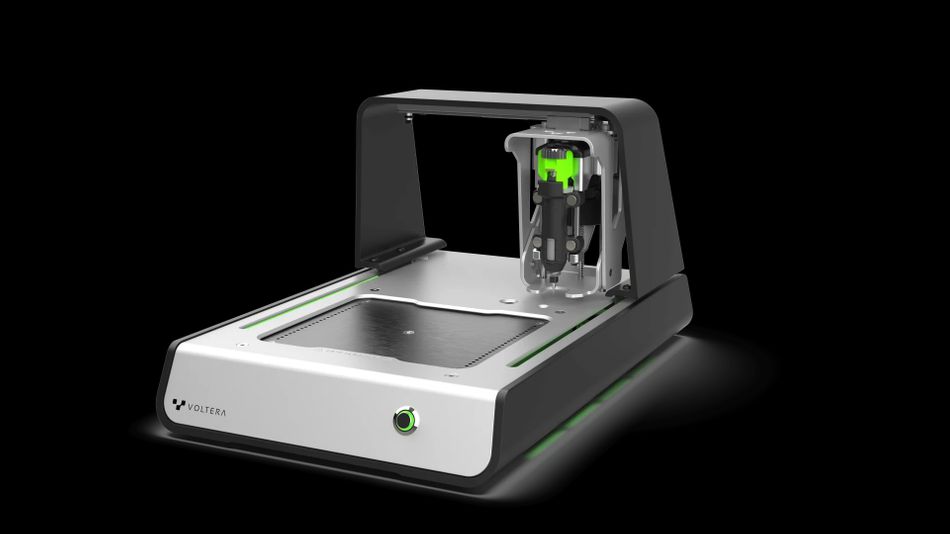
What is the Voltera V-One?
If you’re not familiar with PCB printers, picture them as similar to 3D printers, but instead of creating physical objects, they print intricate circuit patterns onto boards. Just as a 3D printer builds up layers of material to create a three-dimensional object, a PCB printer lays down conductive ink or other materials layer by layer to form the electrical pathways on a circuit board.
Why Choose the V-One for Prototyping?
The V-One offers massive advantages over traditional prototyping processes by integrating PCB printing, drilling, and solder paste dispensing into a single system. This combination cuts iteration time from days and weeks to mere hours, allowing you to identify design errors early and reduce time to market.
The device supports an aligned printing feature, which comes in handy for printing on substrates with pre-existing features. This means you can print on popular development boards like Arduino and Raspberry Pi to create useful add-ons. It’s also perfect for creating double-sided PCBs without any hassle.
The V-One is a plug-and-play machine with user-friendly software. It is powerful enough to be trusted by experts at NASA, yet straightforward enough for a student to quickly learn. Whether you’re a seasoned engineer or just starting out, the V-One is designed for all skill levels.
Prototyping your PCBs in-house has the added perk of keeping your intellectual property safe. When you outsource PCB prototyping, there’s a chance of exposing your designs to unauthorized use, especially if you’re working with suppliers in areas where IP protection isn’t as strong.
Double-Sided PCB Prototyping with the Voltera V-One
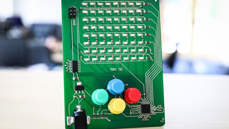
In this tutorial, we’ll walk through the process of creating a double-sided PCB using the Voltera V-One, using a punk console as our example.
Step 1: Prepare and Upload Your Gerber File
You can design your PCB layout using a variety of computer-aided design (CAD) software. The next step is to export your designs in Gerber files. Depending on your software of choice, Voltera offers a detailed Gerber export guide for KiCad, OrCAD, EAGLE, and Altium. Open the V-One software and upload your Gerber file. The software will automatically calculate the tool paths required for your design.
Step 2: Set Up the Printing Surface
Since we’ll be drilling to make a double-sided board, place a sacrificial layer underneath the PCB to protect the bed from any potential damage. Secure the board and sacrificial layer in place by clamping them down onto the printer's bed.
Step 3: Surface Mapping
Attach the proximity probe to the V-One. The software will map the board in XYZ space, preparing it for accurate drilling and trace printing.
Step 4: Drilling
Replace the proximity probe with the drill head. Begin by drilling small holes for vias. Next, drill larger holes for through-hole components. The software will prompt you to change the drill bit as needed.
Step 5: Print Traces on the Top Side
After drilling, clean off any debris from the board’s surface to ensure smooth printing. Swap out the drill head for the dispenser, and allow it to calibrate. Start printing the conductive traces on the top layer. If you notice any mistakes, the V-One offers a selective printing option that allows you to fix specific areas.
Step 6: Curing the Top Side
After printing, remove the sacrificial layer. Flip the board over and rest it on the baking ledges of the clamps. The curing process takes about 40 minutes. Let the board cool down afterward.
Step 7: Print Traces on the Bottom Side
Once the top side has cured, flip the board over to prepare for the bottom side printing. Use the aligned print option in the software, utilizing drilled holes to ensure the top and bottom sides are perfectly aligned.
Begin printing the conductive traces on the bottom side. Cure it using the same procedure as explained in step 6.
Step 8: Add Rivets to Connect Sides
After both sides are printed, use rivets to connect the top and bottom sides at the drilled holes, ensuring proper electrical connectivity between the sides.
Step 9: Dispense Solder Paste
Clamp the board back onto the printer, snap in the proximity probe, and remap the board to ensure accuracy. Replace the probe with the dispenser, this time with a cartridge of solder paste installed, rather than conductive ink. Dispense solder paste onto the designated pads for precise application.
Step 10: Reflow and Solder Components
Place your components on the board and use the heated bed to reflow all surface-mount components in a single step. For through-hole components, use a soldering gun and solder wire to manually solder them in place.
Case Study: Creating a Wearable Device for Robotic Hand Control
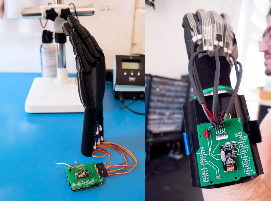
Read how Voltera’s V-One PCB printer and NOVA materials dispensing system enabled a second-year undergrad studying Mechatronics, Robotics, and Automation Engineering at the University of Waterloo to design and build a fully functional robotic hand that mimics the movements of an operator wearing a control glove – in just two months.
Printing Strain Gauges on TPU laminated on a Glove for Remote Hand Control
Industries and applications where the V-One has made a significant impact
Voltera V-One has been making significant contributions across various industries, showcasing its impact on research and development projects.
Advancing Solar Technology
Researchers at The University of Akron used the V-One PCB printer to prototype modular solar (photovoltaic) shingles. Their goal was to create a more efficient manufacturing process using 3D printing and automated circuitry. By leveraging the V-One, they aimed to reduce both the cost and time required compared to traditional manufacturing methods. This innovative approach has the potential to make solar technology more accessible.
Eco-Friendly Supercapacitors
At Tampere University, researchers utilized the V-One alongside additive manufacturing techniques to develop a functional supercapacitor. What sets this project apart is its focus on sustainability. The entire process used only environmentally safe and biodegradable materials. This achievement demonstrates the V-One's ability to drive green technology initiatives.
Aerospace Innovations with CubeSats
The aerospace industry has also benefited from the V-One's capabilities. At Princeton University, the V-One was instrumental in building CubeSats—small, cube-shaped satellites used for space research. These miniature satellites are essential for studying various aspects of space and planetary science. The V-One’s ability to quickly produce PCBs helped streamline the development process, enabling Princeton’s research students to focus on innovation and experimentation.
These partnerships not only showcase V-One's adaptability but also underscore its potential to accelerate research and development in advanced technological fields.
Future-Proofing Your Prototyping Process
How the V-One can be integrated into a larger prototyping workflow
Incorporating the Voltera V-One PCB printer into a broader prototyping workflow can accelerate your product development process. By pairing the V-One with other prototyping tools like 3D printers, you can design and create PCBs along with enclosures or other mechanical parts in-house. This integrated approach not only saves time but also allows for rapid iteration and refinement of designs.
Conclusion
The V-One speeds up the prototyping process significantly. With its ability to quickly print PCBs, drill vias, and dispense solder paste, you can iterate on designs in hours rather than days or weeks. By handling PCB prototyping in-house, the V-One cuts out costly third-party manufacturing and logistics expenses. It also helps protect your designs and intellectual property. Plus, its plug-and-play setup makes it easy to use and shortens the learning curve.
Curious to see how the V-One can fit into your workflow? Book a call with the team at Voltera to explore how this innovative tool can meet your prototyping needs.


