PCB Prepreg vs Core Materials: Engineering Guide to Laminate Selection and Properties
A comprehensive technical analysis of PCB prepreg and core materials, examining their distinct material properties, manufacturing implications, and selection criteria for multilayer PCB design.

13 Nov, 2024. 15 minutes read
Introduction
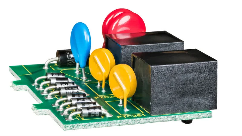
In printed circuit board (PCB) manufacturing, the fundamental distinction between prepreg and core materials forms the backbone of multilayer board construction. While these materials share similar base compositions of glass fiber reinforcement and epoxy resin systems, they serve distinctly different functions in PCB architecture.
Understanding the technical nuances between these materials is essential for engineers, as their properties directly influence the following PCB design parameters in high-performance applications:
Impedance control
Thermal management
Signal integrity
Understanding the Differences between Prepreg and PCB Core
Due to the similarities between prepreg and core, they are often confused. But some fundamental differences set the two apart. With their fully cured resin systems and defined electrical properties, core materials provide the stable foundation layers that host copper circuitry.
On the other hand, the prepreg is partially dried without lamination and is less rigid than the core. Prepreg, containing partially cured resin, is the critical bonding agent that fuses multiple core layers during lamination. Simply put, the core is created by laminating prepreg, making it significantly more rigid. The core consists of a flame-retardant fiberglass-epoxy laminate with copper layers on both sides.
Another key difference is their dielectric constant: the core’s dielectric constant is stable, while that of the prepreg changes before and after lamination. This variation in dielectric constants depends on factors such as resin content, resin type, and glass weave.
The selection and implementation of appropriate prepreg and core materials significantly impact manufacturing yields, electrical performance, and long-term reliability of multilayer PCBs, particularly in high-frequency and high-speed digital designs where material properties become increasingly critical.
Suggested Reading: What is a Multilayer PCB?
What are Prepreg Materials?
Prepreg is a conductive material that provides necessary insulation between the PCB’s copper and core. It is a dielectric substance that is placed between two cores or between a core and a copper foil, often referred to as a binding material because it bonds either two cores or a core and copper foil together.
As the name suggests, prepreg is a glass fiber infused with a resin bonding agent. All prepregs are B-stage materials, and they come in various types depending on their thickness and resin content. Prepregs are generally available in three categories based on resin content:
Standard Resin
Medium Resin
High Resin
The typical preparation process for prepreg includes:
Reinforcement with resins
Removal of excess resin
Curing preparation with both high- and low-temperature settings
Prereg Material Types
Various types of prepreg materials are available, each with distinct properties suited to specific applications. Some of the most common prepreg materials include:
FR-4 Prepreg - The most widely used prepreg in the PCB industry, FR-4 (Flame Retardant 4) is made from woven fiberglass fabric impregnated with an epoxy resin. It offers strong mechanical properties, excellent dimensional stability, and reliable electrical insulation, making it suitable for a broad range of PCB applications.
High Tg Prepreg - High Tg (Glass Transition Temperature) prepreg materials are engineered to withstand higher temperatures than standard FR-4. They are commonly used in applications that require enhanced thermal stability, such as in automotive, aerospace, and military electronics.
Low Dk/Df Prepreg - Low Dk/Df (Dielectric Constant and Dissipation Factor) prepregs are designed to reduce signal loss and distortion in high-frequency applications. With a lower dielectric constant and dissipation factor than standard FR-4, these materials are ideal for high-speed digital and RF/microwave applications.
Flexible Prepreg - This prepreg type provides flexibility and bendability for the final PCB, making it well-suited for applications requiring conformability, such as wearable electronics, flexible displays, and medical devices.
Suggested Reading: Rigid Flex PCB: Revolutionizing Modern Electronics Design
What are Core Materials?
The core material of a circuit board serves as the foundational layer, providing essential structural support and stability for the entire PCB. This core layer is what ultimately gives the board its rigidity and strength, allowing it to withstand mechanical stress and maintain its shape.
Typically, the core material is composed of one or more layers of prepreg, which are subjected to processes like pressing, hardening, and heat curing. These prepreg layers are usually made from FR4 materials, such as fiberglass-epoxy laminates, which meet specific flame-retardant standards, ensuring safety and durability in various applications.
The core is also coated with copper foil on both sides, a feature that leads to its designation as "copper-clad laminate." This copper coating forms the conductive pathways necessary for electrical connections across the PCB layers. In some designs, however, the core may only have copper lamination on one side, depending on the application’s requirements and design specifications.
Key Considerations for Picking PCB Core Materials?
PCB core materials must be carefully selected, and the following are the basic critical considerations for the material selection:
Impedance Control - For high-speed and high-frequency circuits to maintain a stable dielectric constant as frequencies fluctuate.
Thermal Properties - To prevent delamination, decomposition, or layer separation issues in temperature-sensitive applications.
Electrical Properties - To ensure reliable electric performance with a low-dielectric constant, ideal for insulating conductive traces and power planes.
Chemical Properties - For resistance to moisture and chemical absorption to maintain consistent electrical performance over time.
Dimensional Stability - To counter temperature changes, electrical surges, mechanical shocks, and physical stress.
Signal Performance - Different materials absorb signals at varying rates. For high-frequency PCBs, the core should have a low dissipation factor to reduce signal loss and improve overall signal quality.
Material Composition and Structure
Chemical Composition Analysis
The fundamental chemistry of PCB materials centers on epoxy resin systems and glass fiber reinforcement. Prepreg materials utilize B-stage epoxy resins, containing 35-65% partially polymerized resin content. Core materials employ fully cured C-stage resins with cross-linking density >90%. The primary resin systems include:
Standard FR-4: tetrafunctional epoxy
High-Tg FR-4: Multifunctional epoxy
Modified epoxy systems: Phenolic-enhanced structures
Glass fabric specifications vary between materials:
Style | Weight (g/m²) | Thickness (μm) | Common Use |
106 | 25 | 38 | Thin cores |
1080 | 47 | 64 | Prepreg |
2116 | 96 | 99 | Thick cores |
7628 | 203 | 173 | Power planes |
Material Composition Comparison:
Component | Prepreg | Core |
Resin State | B-stage (partial) | C-stage (full) |
Resin Content | 35-65% | 40-45% |
Glass Style | 106, 1080, 2116 | 2116, 7628 |
Filler Content | 0-15% | 5-20% |
Flow Properties | High flow | No flow |
The glass reinforcement consists of E-glass fibres (52-56% SiO₂, 12-16% Al₂O₃, 16-25% CaO) woven into specific styles.
The fiber diameter ranges from 5-7μm, with surface treatment using silane coupling agents for optimal resin adhesion.
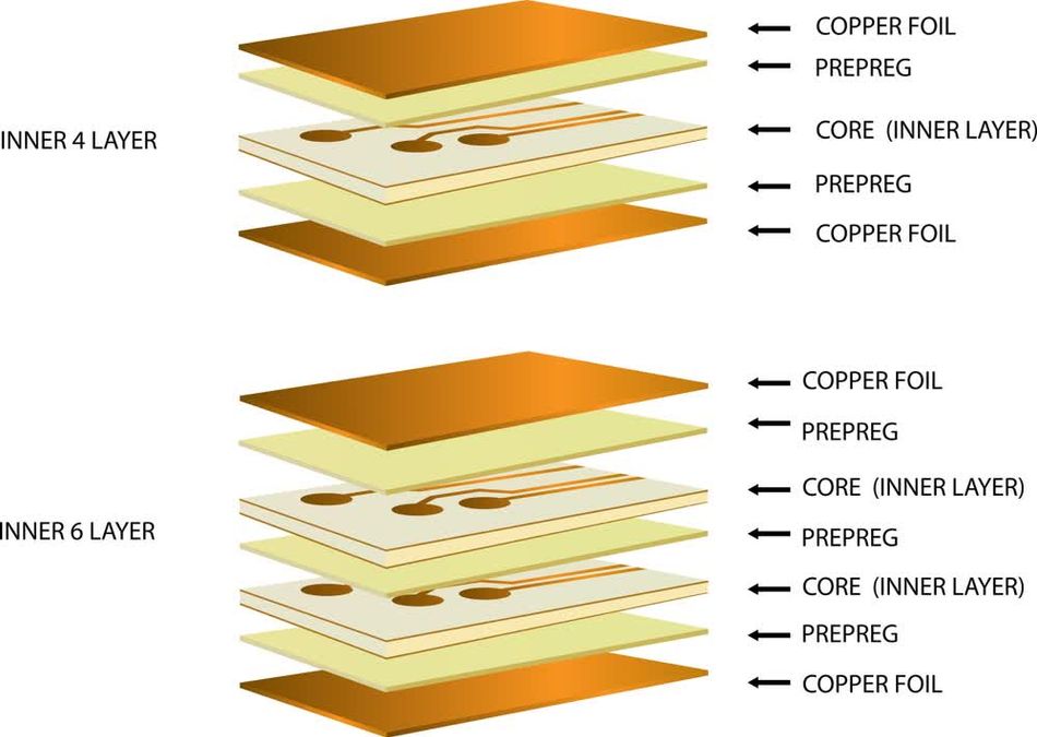
Physical Structure Characteristics
The cross-sectional structure of prepreg and core materials exhibits distinct layered configurations. Core materials maintain a rigid, fully cured structure with a copper foil bonded to both sides, while prepreg layers possess a more malleable structure before final lamination.
Cross-sectional view of typical PCB layers:
The curing process progresses through distinct stages:
A-stage: Initial liquid resin state
B-stage (Prepreg): 35-65% cross-linking, tacky consistency
C-stage (Core): >90% cross-linking, fully cured state
Density variations correlate with glass style and resin content:
Core density: 1.80-2.00 g/cm³
Prepreg density (pre-cure): 1.65-1.85 g/cm³
Post-lamination density: 1.85-2.05 g/cm³
Thickness tolerances maintain strict specifications:
Core: ±10% of nominal thickness
Prepreg: ±15% pre-lamination
Post-lamination: ±5% total thickness
Microscopic examination reveals distinct characteristics:
Glass fiber diameter: 5-7μm
Weave patterns: Plain (1x1) or spread weave
Resin distribution: Uniform in cores, variable in prepreg
Void content: <1% in cores, 2-5% in prepreg
Interface thickness: 1-3μm between glass and resin
Electrical Properties
The dielectric properties of prepreg and core materials fundamentally determine PCB performance in high-speed applications. These materials exhibit frequency-dependent characteristics that directly impact signal transmission.
Dielectric Constants (Dk)
The structural differences in core and prepreg materials make it crucial to accurately determine the dielectric constant and loss tangent, especially for signal integrity in high-frequency designs. While for low-speed signals, values from datasheets may suffice, GHz-range signals require more precision.
This variability occurs because PCB materials are inhomogeneous and anisotropic, with properties affected by the fiber weave pattern, leading to effects like skew and fiber cavity resonances. Material thickness also matters for signal behavior, as the effective dielectric constant—a complex parameter—depends on trace dimensions and layer thickness.
Suggested Reading: Understanding PCB Thickness: A Comprehensive Guide
Material Type | Dk @100MHz | Dk @1GHz | Dk @10GHz |
Standard Core | 4.2-4.4 | 4.0-4.2 | 3.8-4.0 |
High-Tg Core | 4.0-4.2 | 3.8-4.0 | 3.6-3.8 |
Prepreg | 4.0-4.6 | 3.8-4.4 | 3.6-4.2 |
Dissipation Factor at Various Frequencies:
Low Dk/Df (Dielectric Constant and Dissipation Factor) prepreg materials are specifically engineered to reduce signal loss and distortion in high-frequency applications. These materials are essential for maintaining signal integrity at high frequencies, where standard materials may fall short.
With a lower dielectric constant and dissipation factor than standard FR-4 prepreg, Low Dk/Df materials are particularly suited for high-speed digital and RF/microwave applications. Their properties make them ideal for use in circuits requiring reliable performance and minimal interference at elevated frequencies.
Material Type | Df @100MHz | Df @1GHz | Df @10GHz |
Standard Core | 0.015 | 0.018 | 0.022 |
High-Tg Core | 0.012 | 0.015 | 0.019 |
Prepreg | 0.016 | 0.019 | 0.024 |
Impedance Control Parameters
Particularly in high-speed and high-frequency circuits, there is a need for tight impedance control. It ensures that the dielectric constant remains stable with change in frequencies. In terms of impedance control, the manufacturers have more control with the core layers as they are easier to reproduce as compared to prepreg.
On the other hand, the prepreg material dielectric constant can only be specified for the raw material and not after the assembly. Hence, the true dielectric constant experienced by the electric signal can never be predicted.
Dielectric thickness tolerance: ±10%
Copper roughness factor: 1.5-2.0
Impedance tolerance: ±10%
Signal Integrity Considerations
Signal integrity is one of the most critical physical parameters as it directly affects PCB performance. All materials have a different signal absorption rate. In case of a high-frequency PCB, the core is more conducive as it has a low dissipation factor. Hence, the signal losses are greatly minimized.
Maximum crosstalk: -30dB @1GHz
Insertion loss: -0.5dB/inch @1GHz
Return loss: -20dB minimum
Propagation delay: 180ps/inch ±10%
Rise time degradation: <10% for 1ns rise time
The frequency-dependent behavior affects:
Signal attenuation: 0.1-0.5 dB/inch/GHz
Phase stability: ±5° maximum variation
Group delay: <±5ps variation
Bandwidth limitations: Effective up to 20GHz
Mechanical Properties
The mechanical characteristics of PCB materials directly influence board reliability and manufacturing yield. Tensile strength measurements conducted according to IPC-TM-650 2.4.19 demonstrate significant variations between prepreg and core materials.
Suggested Reading: IPC Class 2 vs Class 3: Understanding the Critical Differences in Electronics Manufacturing Standards
Tensile Strength Specifications
Core Materials (Machine Direction): 380-420 MPa
Core Materials (Cross Direction): 340-380 MPa
Prepreg (Pre-cure, Machine Direction): 280-320 MPa
Prepreg (Post-cure, Machine Direction): 360-400 MPa
Coefficient of Thermal Expansion (CTE)
Direction | Core Material | Prepreg (Post-cure) |
X-axis | 14-16 ppm/°C | 16-18 ppm/°C |
Y-axis | 14-16 ppm/°C | 16-18 ppm/°C |
Z-axis | 50-60 ppm/°C | 55-65 ppm/°C |
Flexural Strength Measurements
Material Type | Room Temp. | 150°C |
Core | 550 MPa | 480 MPa |
Prepreg | 520 MPa | 450 MPa |
Dimensional Stability Parameters
Length/Width Change: ±0.10% maximum
Thickness Change: ±5% maximum
Bow and Twist: 0.75% maximum
Post-etching Shrinkage: <0.15%
Thermal Stress Resistance: >10 seconds at 288°C
Comprehensive Mechanical Properties
Property | Core | Prepreg |
Young's Modulus (GPa) | 22-24 | 20-22 |
Peel Strength (N/mm) | >1.4 | >1.2 |
Glass Transition Temp (°C) | 170-180 | 165-175 |
Decomposition Temp (°C) | >330 | >320 |
Moisture Absorption (%) | <0.20 | <0.25 |
Specific Gravity | 1.85-1.95 | 1.80-1.90 |
Hardness (Rockwell) | >M95 | >M90 |
Manufacturing Process Integration
Processing Parameters
Temperature and pressure requirements for PCB lamination processes demand precise control throughout the manufacturing cycle. The lamination press operates under specific parameters shown in the following table:
Temperature Requirements | Pressure Specifications | Cure Cycle Specifications |
|
|
|
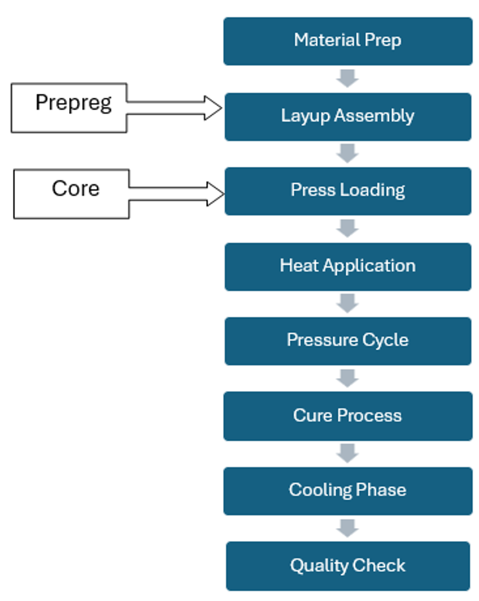
The lamination process flow can be seen in the following figure:
The Critical Control Points during the lamination process flow are described in the following table:
Material Preparation | Layup Process | Press Parameters | Post-Cure Verification |
|
|
|
|
Quality Assurance
PCB material quality assurance requires systematic inspection protocols and precise measurement techniques following IPC-4101 specifications. Inspection methods employ both destructive and non-destructive testing approaches to ensure material integrity.
Primary Inspection Methods
Visual Inspection
Surface defects examination
Color uniformity assessment
Foreign material detection
Registration mark alignment
Microsection Analysis
Glass/resin distribution
Void content measurement
Interface examination
Layer thickness verification
Suggested Reading: Mastering PCB Testing: Techniques, Methods, and Best Practices Unveiled
Quality Metrics and Acceptance Criteria
Parameter | Core Material | Prepreg |
Thickness Tolerance | ±10% | ±15% (pre-cure) |
Resin Content | 40-45% | 35-65% |
Glass Content | 55-60% | 35-65% |
Volatile Content | <0.3% | <0.5% |
Copper Adhesion | >1.4 N/mm | >1.2 N/mm |
Tg Deviation | ±5°C | ±8°C |
Troubleshooting Guidelines
Delamination Issues
Check moisture content
Verify cure temperature profile
Examine pressure distribution
Review material storage conditions
Registration Problems
Verify material acclimation
Check tooling hole accuracy
Assess dimensional stability
Monitor pressure application
Thickness Variations
Review pressure settings
Check material distribution
Verify stack-up calculations
Examine press plate flatness
QC Checkpoint Checklist
To enhance proper quality check, it’s important to ensure multiple checkpoints. Here are some points to consider:
Incoming Material Inspection - This step ensures the quality of materials received for PCB production. Key checks include verifying the moisture content of materials, conducting a thorough visual examination for defects, reviewing compliance documentation, and confirming that storage conditions meet specified requirements.
Pre-lamination Checks - Before lamination, additional inspections ensure materials are prepared properly. This includes monitoring the staging time of materials, checking that environmental conditions are controlled, ensuring tools are clean, and confirming the correct orientation of materials for the lamination process.
Process Monitoring - During the lamination process, critical parameters are tracked to maintain quality standards. These include monitoring the temperature profile, pressure readings, and vacuum levels, along with verifying that the cycle time meets specified requirements to ensure consistency and reliability in the final product.
Common Defect Analysis Methods
The following table summarises the multiple defect analysis methods for high-quality PCB production:
Cross-sectional Analysis | Surface Analysis | Thermal Analysis |
|
|
|
Design Implementation Guidelines
Stack-up Design
Stack-up design rules for PCB manufacturing require precise material selection and layer arrangement to achieve optimal electrical and mechanical performance. The fundamental principles govern signal integrity and impedance control across multiple layers.
Basic Stack-up Rules:
Maintain symmetrical construction
Alternate signal and plane layers
Balance copper distribution
Include ground reference planes
Maintain minimum dielectric spacing
Impedance Calculation Guidelines:
The following equations may be used for calculating the characteristic impedance of PCB materials:

Where:
Z₀ = Characteristic impedance
εᵣ = Dielectric constant
H = Dielectric height
W = Trace width
T = Copper thickness
Thickness Planning Matrix:
Layer Type | Material | Thickness (μm) |
Outer Copper | Foil | 35-70 |
Prepreg | 1080 | 64-71 |
Core | FR-4 | 100-200 |
Inner Copper | Foil | 17-35 |
Layer Thickness Calculation:
Start with the finished board thickness
Subtract outer copper layers
Calculate core thicknesses
Determine prepreg requirements
Verify total stack-up height
Common Design Pitfalls:
Asymmetrical construction leading to warpage
Insufficient spacing between power/ground planes
Improper prepreg selection for impedance control
Mismatched CTE between materials
Poor reference plane allocation
Incorrect dielectric thickness for impedance
Insufficient consideration of material properties
Overlooking manufacturing tolerances
Improper signal layer pairing
Poor copper balance across layers
Ignoring a design review during the initial stages.
Suggested Reading: The Five Biggest Design Mistakes for PCB Assemblies
Material Selection Framework
Material selection for PCB manufacturing requires systematic evaluation of multiple parameters to achieve optimal performance within specified constraints. The decision matrix encompasses electrical, mechanical, and thermal properties alongside manufacturing considerations.
Material Selection Decision Matrix:
Criteria Category | Weight | FR-4 | High-Tg FR-4 | Modified Epoxy |
Electrical | 30% | 3/5 | 4/5 | 5/5 |
Thermal | 25% | 3/5 | 4/5 | 4/5 |
Mechanical | 20% | 4/5 | 4/5 | 3/5 |
Cost | 15% | 5/5 | 3/5 | 2/5 |
Processability | 10% | 5/5 | 4/5 | 3/5 |
Application-Specific Requirements:
High-Speed Digital | RF/Microwave | Power Applications |
|
|
|
Environmental Considerations:
RoHS Compliance
Lead-free compatibility
Halogen-free options
Bromine content <900 ppm
Chlorine content <900 ppm
Environmental Impact
Energy consumption in manufacturing
Recyclability potential
Waste reduction capability
End-of-life disposal
Sustainability Metrics
Carbon footprint
Water usage
Chemical emissions
Resource depletion
Conclusion
The selection and implementation of PCB prepreg and core materials fundamentally influence the performance, reliability, and manufacturability of multilayer printed circuit boards. Understanding the distinct characteristics, processing requirements, and quality control measures ensures optimal material selection and successful PCB manufacturing outcomes.
Frequently Asked Questions
1. What are the key differences in dielectric properties between prepreg and core materials?
Core materials typically exhibit more stable dielectric constants (Dk) due to their fully cured state, with variations of ±5% compared to prepreg's ±10%. At 1GHz, standard FR-4 cores maintain Dk values of 4.0-4.2, while prepregs range from 3.8-4.4. This difference stems from the B-stage nature of prepreg materials and their varying resin content (35-65% versus core's 40-45%). Reference: IPC-4101E specifications.
2: How do processing temperatures affect prepreg flow characteristics?
Prepreg materials exhibit distinct flow characteristics across three temperature ranges:
Initial Flow (85-105°C): Resin viscosity begins decreasing
Gel Point (130-140°C): Optimal flow window for void-free lamination
Final Cure (175-185°C): Cross-linking completion Processing must maintain 250-300 PSI pressure during the flow window to achieve proper resin distribution. Reference: IPC-4101E/126 processing guidelines.
3. What are the essential quality control parameters for incoming material inspection?
Key QC parameters include:
Moisture content: <0.2% for prepreg, <0.1% for core
Glass transition temperature (Tg): ±5°C from specification
Resin content: Within ±3% of nominal value
Thickness tolerance: ±10% for core, ±15% for prepreg
Surface quality: No scratches >0.1mm depth Reference: IPC-4101E/126 acceptance criteria.
4. How can delamination issues be effectively diagnosed and prevented?
Delamination prevention requires:
Moisture content verification: <0.2% maximum
Proper storage conditions: 20-23°C, 45-55% RH
Optimal pressure application: 350-400 PSI during cure
Adequate prepreg staging time: <4 hours at room temperature
Correct cure temperature profile: ±2°C tolerance Reference: IPC-6012E, Class 3 requirements.
5. What are the critical factors for achieving reliable copper-to-dielectric adhesion? A6: Essential factors include:
Surface preparation: Minimum 1μm roughness
Oxide treatment type: Reduced oxide preferred
Lamination pressure: Minimum 250 PSI
Temperature ramp rate: 1.5-2.5°C/minute
Post-cure cooling rate: Maximum 3°C/minute Reference: IPC-4101E adhesion requirements.
Reference:
Prepreg vs. Core: What Are Their Role in PCB Manufacturing – PCB COPY
Adhesion of Epoxy Resin with Hexagonal Boron Nitride and Graphite - Scientific Figure on ResearchGate. Available from: https://www.researchgate.net/figure/Chemical-structure-of-a-epoxy-resin-and-b-its-fragment-models_fig2_331461924 [accessed 12 Nov 2024]
https://resources.altium.com/p/pcb-core-vs-prepreg-material-what-designers-need-to-know