How to Scale Manufacturing with ESD-safe 3D Printing?
Addressing the risks and challenges of electrostatic discharge in manufacturing thanks to innovative 3D printing materials.
06 Apr, 2023. 7 minutes read

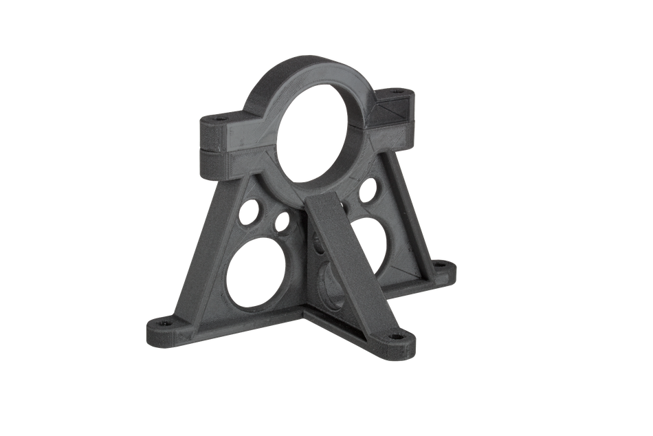
Caption: Ultrasint® PA11 ESD, printed part. Source: BASF.
What is Electrostatic discharge?
Electrostatic discharge (ESD) is the sudden transfer of electrical charge that occurs between two objects at different electric potentials. A material can accumulate a static charge as a result of a phenomenon known as triboelectric charging, in which a transfer of electrons occurs between two bodies.(1)
The likelihood of triboelectric charging depends on the different compositions of the two materials and can be predicted using the “triboelectric series”.(2) This is a table that ranks materials based on their tendency to lose or gain electrons. Once an object is electrostatically charged, as it approaches a conductive body at a different electrostatic potential, electrons rapidly flow from one body to the other, triggering a spark.
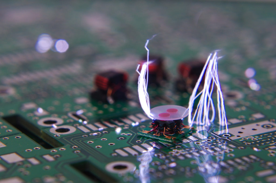
ESD is an everyday experience for all of us: we have all experienced the electric “zap” that can occur when touching a metallic object after walking on carpet while wearing shoes. The reason why this happens is that our skin and most synthetic materials are located at opposite ends of the triboelectric series. As a result, you can easily accumulate several kilovolts of charge on your body during everyday activities.
Although ESD is a relatively harmless phenomenon in everyday life, it can have serious consequences. As early as the 1400s, for example, military forts already employed ESD safety procedures to prevent the danger of involuntary ignition of gunpowder by static electricity.(1) Today, ESD safety is a critical concern in manufacturing industries. It is especially significant in the context of the electronic industry, where ESD-sensitive devices can be seriously affected.(3)
As smaller and more complex geometries are introduced, electronics have become increasingly vulnerable to ESD damage.(4)
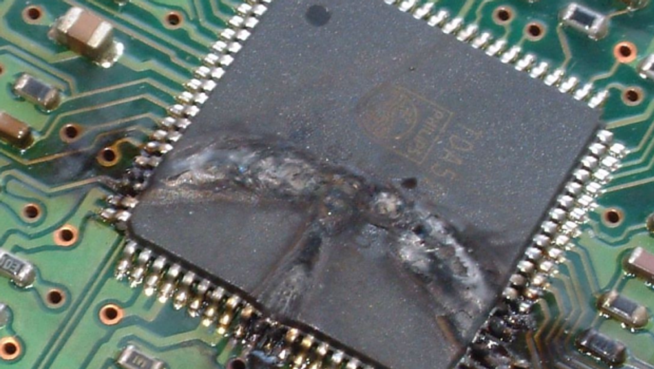 Example of ESD damage to electronic components. Source: TechnofaqESD-safety and Risks in Manufacturing
The ESD association estimates that between 8% and 33% of all electronic devices are lost as a result of ESD damage, with a total cost in the range of billions of dollars each year.(1) The effects of ESD include the damage or destruction of electronic components, the erasure or alteration of magnetic memories, and the ignition of flammable material.
Damage from ESD can occur in several moments during the lifetime of an electronic device. It can take place during the manufacturing process, during maintenance, or during field service. It is estimated that under the threshold of 2 kV, ESD cannot be perceived directly by humans.(2) As a result, electronic components such as diodes and chips may be significantly damaged during handling without the operator’s knowledge and only show the effects of malfunctioning later on.
ESD events that affect electronics may be classified into three different categories.(1)
- Discharge to the device. In this case, the electrostatic charge is transferred from a charged conductor, often the human body, to the component.
- Discharge from the device. The charge is transferred from the item to any conductor. Components or devices can accumulate electrostatic charge during handling, processing, packaging, or transport, and discharge it later on.
- Field-induced discharges. In this case, the ESD event is triggered by an external electrostatic field.
ESD damage in electronics is typically classified as either catastrophic failure, parametric failure, or latent failure.(5) In catastrophic failure, the component or device is damaged to the point it no longer functions. This may be due to metal melt, junction breakdown or oxide breakdown as a consequence of the ESD spark. Parametric failure refers to a detectable loss of performance that does not fully affect the operation of the device. Latent failure, on the other hand, consists in undetectable damage that results in failure after a period of normal operation.
A device or component may be partially degraded by ESD while still performing its intended function, although this can significantly reduce its operating life, leading to premature failure. Latent ESD damage is especially difficult to detect and repair after the components are assembled in a finished product.
3D-printing materials and ESD-safety
To understand ESD safety, it is important to focus on the properties of materials first. In the context of electrostatic properties, all materials can be categorized based on their surface resistance. Surface resistance is a parameter that measures the ability of a material to resist the flow of current along its surface.
Based on this parameter, materials may be categorized as either conductive (such as metals), insulative (such as plastics) or static dissipative. ESD-safe materials need to fall in the static dissipative range, with a surface resistivity between 105 and 1011 Ω/m2.(2) This allows the static charge to be transferred slowly away from the component without generating sparks.
Most electronic devices, including smartphones, televisions, and laptops, need ESD-safe housing to prevent damage from static electricity. However, the materials for these components need to be carefully selected. Neither conductive nor insulative materials are appropriate choices. While plastic doesn’t conduct electricity, it can store electrostatic charges for long periods of time and trigger ESD events.
Most materials typically used in 3D printing are insulative materials. Therefore, you should not overlook the risk of ESD damage with 3D-printed parts. However, the electrical properties of 3D-printing materials can be tuned thanks to the inclusion of specific additives, such as carbon-based materials.(6)
The addition of carbon to polymeric materials such as polyamide, nylon and resins can turn them from insulative to static dissipative. Carbon additives used in ESD-safe 3D printing materials range from traditional materials such as carbon black or carbon fiber to advanced nanomaterials such as graphene or carbon nanotubes.
In the context of 3D printing, it is important to consider how the manufacturing process impacts the electrical properties of materials and the likelihood of ESD damage. Printing temperature can significantly alter the expected surface resistivity of the component.(6) Typically, as the temperature is increased, resistivity also increases and the printed part will become more insulative. Furthermore, raster spacing and orientation during printing can also influence the conductivity of the printed component.
Because of this, you should always keep in mind that ESD safety is not guaranteed by the printing material. Instead, each printed part should be individually assessed.
BASF ESD-safe 3D Printing Solutions
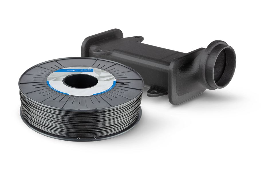
Introducing ESD safety to additive manufacturing requires the use of advanced materials with tailored electrical properties.(7) The BASF ForwardAM portfolio offers you a range of materials designed to address this technological challenge. Two main materials were developed by BASF for ESD-sensitive applications: one in powder (Ultrasint® PA11 ESD) and one in filaments (Ultrafuse® PAHT CF15).
Ultrasint® PA11 ESD is a bio-derived polyamide-based material produced from castor oil. All materials in the Ultrasint® portfolio exploit Powder Bed Fusion (PBF) technology for part manufacturing. In particular, Ultrasint® PA11 ESD is designed for the Selective Laser Sintering (SLS) technique. SLS is a 3D printing technology that utilizes a precise laser to heat and fuse layers of fine powder together. This additive manufacturing process is repeated layer by layer until the part is fully formed.
Ultrasint® PA11 ESD is designed to favor the discharge of static electricity from components and devices sensitive to ESD damage. In addition to its dissipative properties, Ultrasint® PA11 ESD retains some of the exceptional mechanical and surface quality advantages of Ultrasint® PA11. Besides offering optimal ESD properties, this advanced manufacturing material also exhibits outstanding mechanical properties, with high tensile strength and elasticity, as well as high process stability.
The combination of these properties makes Ultrasint® PA11 ESD the ideal material for manufacturing protective housings for electronic devices. Furthermore, Ultrasint® PA11 ESD can be used to design jigs and fixtures for manufacturing to prevent ESD damage to circuit boards and other electronic components during processing. Finally, you can use Ultrasint® PA11 ESD to optimize tooling processes and machine parts.
If you’re looking to improve ESD safety in Fused Filament Fabrication (FFF), Ultrafuse® PAHT CF15 may be the material for you. This high-temperature polyamide-based material contains 15% carbon fiber additive and can be used with any FFF printer with a hardened nozzle.
Ultrafuse® PAHT CF15 is a static dissipative material ideal for ESD-sensitive applications. The presence of carbon fiber improves the temperature resistance, chemical resistance, dimensional stability and mechanical properties of printed components. This high-performance material is suited for printing complex parts in challenging operating environments.
For example, Ultrafuse® PAHT CF 15 is compatible with water-soluble support materials such as Ultrafuse® BVOH. This enables the printing of elaborate designs with temporary support structures.
By leveraging the unique properties of BASF’s diverse materials portfolio, you can extend the manufacturing benefits of 3D printing to the most ESD-sensitive applications, ensuring reliable and efficient manufacturing every time.
References
[1] EOS/ESD Association. Fundamentals of Electrostatic Discharge, Part One: An Introduction to ESD, EOS/ESD Association. Inc., Rome, NY [Internet]. 2020. Available from: https://www.esda.org/esd-overview/esd-fundamentals/part-1-an-introduction-to-esd/
[2] Mardiguian, M. Electrostatic Discharge. Understand, Simulate, and Fix ESD Problems, 3rd ed. Piscataway (NJ): IEEE Press; 2009.
[3] Voldman SH. A review of electrostatic discharge (ESD) in advanced semiconductor technology. Microelectronics Reliability. 2004; 44:33-46.
[4] Electronic Products. Matching ESD Protection to Process Geometry. Electronic Products [Internet]. 2012 Apr 21. Available from: https://www.electronicproducts.com/matching-esd-protection-to-process-geometry/
[5] National Aeronautics and Space Administration (NASA). Workmanship Manual For Electrostatic Discharge Control. NASA [Internet]. 2010. Available from: https://standards.nasa.gov/sites/default/files/standards/NASA/Baseline/0/nasa-hdbk-873921.pdf
[6] Shields, G. Protect Your Electronics with ESD-Safe 3D Printing Material. All3DP [Internet]. 2022 May 3. Available from: https://all3dp.com/1/protect-your-electronics-with-esd-safe-3d-printing-material/
[7] Kohut, A. ESD-safe Materials: A Beginner’s Guide. Wevolver [Internet]. 2021 Aug 02. Available from: https://www.wevolver.com/article/esd-safe-materials-a-beginners-guide